Embed Size (px)
Citation preview

F1.1 Kalt, Lemmer
1
Subproject F1.1
New Concepts for hybrid solar cells Principle Investigators: Uli Lemmer and Heinz Kalt CFN-Financed Scientists: Further Scientists: Jonas Conradt, Manuel Reinhard, Andreas Pütz, Alexander Colsmann, Janos Sartor, Florian Maier-Flaig, Johannes Fallert Institut für Angewandte Physik Karlsruher Institut für Technologie (KIT) Lichttechnisches Institut Karlsruher Institut für Technologie (KIT)
F1.1 Kalt, Lemmer
2
New concepts for hybrid solar cells Contents:
1. Motivation 2. ZnO nanorod arrays for hybrid solar cells
a. Synthesis b. Characterization of the nanorods c. Hybrid solar cells incorporating ZnO nanorods d. Conclusion
3. Indium-doped ZnO nanoparticles a. Experimental / Synthesis b. Inverted solar cells comprising IZO buffer layers c. Tandem solar cells d. Conclusion
4. Outlook
1. Motivation Since the first evidence of photoinduced charge generation in conjugated polymer/fullerene composites [1], the research field of organic solar cells based on these materials has attracted enormous scientific and industrial interest. Like in other thin-film solar technologies such as amorphous silicon-based photovoltaics, the most promising approach for highly efficient organic solar cells is the so-called p-i-n architecture comprising an intrinsic absorber layer sandwiched by p- and n-doped charge transport layers [2]. While there are some solution-processable and air-stable p-doped semiconductors such as Poly(3,4-ethylenedioxythiophene):poly(styrenesulfonate) (PEDOT:PSS) or doped Polyaniline, there is still a lack of n-doped counterparts [3,4]. Thus, state-of-the-art organic solar cells mostly comprise n-type metal oxides like titanium dioxide (TiO2)[5] or zinc oxide (ZnO)[6]. While TiO2 can hardly be n-doped ZnO can easily be doped by incorporation of indium or aluminum [7]. ZnO tends to form nanostructures by self-assembly under appropriate growth conditions [8]. The possibility to synthesize tailored nanostructures makes this semiconductor especially interesting for the use in hybrid solar cells and thus it was chosen as inorganic component. In order to realize hybrid solar cells with ZnO as inorganic component, two strategies are pursued in this project. The first approach bases on the incorporation of zinc oxide nanorod arrays into the device. The commonly utilized bulk heterojunction absorber comprises a blend of a polymeric donor material and a fullerene derivative as electron acceptor. However, the morphology of such mixtures can only be modified by indirect treatment such as thermal annealing [9] or slow growth methods [10]. Thus, the introduction of a nanostructured interlayer can be a viable approach in order to directly manipulate the nanomorphology of the photoactive blend. The arrays are synthesized using a catalyst-free vapor-transport growth method at 510°C, which allows for the growth of highly crystalline, well-aligned ZnO nanorod arrays with a tunable length, ranging from hundreds of nanometers to several micrometers [8]. The nanorods exhibit an excellent crystal quality, as shown by photoluminescence measurements and high-resolution transmission electron microscopy. Optical transmission spectra show a sufficient transparency of the substrates,
F1.1 Kalt, Lemmer
3
qualifying them for photovoltaic applications. Hybrid solar cells incorporating these nanostructured substrates were developed and characterized. For the second approach thin, compact layers of indium-doped ZnO (IZO) nanoparticles are used serving as inorganic n-doped semiconductor material. IZO nanoparticles are synthesized by a method based on microwave-assisted polyol synthesis developed in CFN project F1.3. The incorporation of indium as dopant into the ZnO nanoparticles allows for proper energetic alignment between the absorber blend and the cathode. Hence, we fabricate inverted hybrid solar cells exhibiting energy conversion efficiencies of up to 2.3%. We further present hybrid recombination zones comprising a stack of a PEDOT:PSS layer and an IZO nanoparticle layer allowing for the fabrication of hybrid tandem solar cells.
2. ZnO nanorod arrays for hybrid solar cells
For photovoltaic applications, high-temperature, carbothermal methods known to result in excellent crystalline quality of the nanostructures [11] can be excluded as the TCO substrate is irreversibly damaged by the thermal stress. However, hydro-thermal or chemical low-temperature processes generally result in nanostructures with a lower crystal quality as reported by Greene et al.[12] Further, many nanostructures reported in the literature are grown on indium-doped tin oxide (ITO) substrates. Here, economic problems are pending due to the limited availability of the resource indium. Obviously, there is a need for a solar cell technology based on alternative TCOs, such as aluminum-doped ZnO (AZO) allowing the growth of high quality ZnO nanostructures. In this section, the synthesis (2.a) and the characterization of the ZnO nanorods (2.b) is presented, which are then tested within hybrid solar cells (2.c).
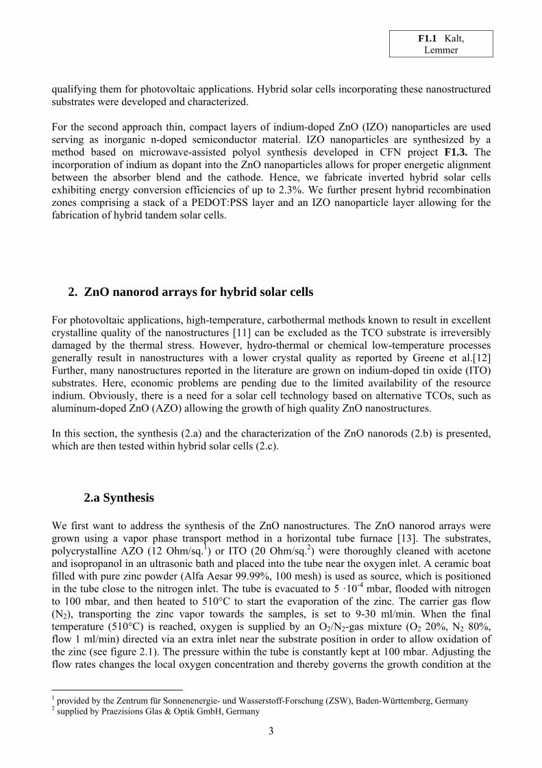
2.a Synthesis We first want to address the synthesis of the ZnO nanostructures. The ZnO nanorod arrays were grown using a vapor phase transport method in a horizontal tube furnace [13]. The substrates, polycrystalline AZO (12 Ohm/sq.1) or ITO (20 Ohm/sq.2) were thoroughly cleaned with acetone and isopropanol in an ultrasonic bath and placed into the tube near the oxygen inlet. A ceramic boat filled with pure zinc powder (Alfa Aesar 99.99%, 100 mesh) is used as source, which is positioned in the tube close to the nitrogen inlet. The tube is evacuated to 5 ·10-4 mbar, flooded with nitrogen to 100 mbar, and then heated to 510°C to start the evaporation of the zinc. The carrier gas flow (N2), transporting the zinc vapor towards the samples, is set to 9-30 ml/min. When the final temperature (510°C) is reached, oxygen is supplied by an O2/N2-gas mixture (O2 20%, N2 80%, flow 1 ml/min) directed via an extra inlet near the substrate position in order to allow oxidation of the zinc (see figure 2.1). The pressure within the tube is constantly kept at 100 mbar. Adjusting the flow rates changes the local oxygen concentration and thereby governs the growth condition at the
1 provided by the Zentrum für Sonnenenergie- und Wasserstoff-Forschung (ZSW), Baden-Württemberg, Germany 2 supplied by Praezisions Glas & Optik GmbH, Germany
F1.1 Kalt, Lemmer
4
sample position. After approximately 15 min, the heating is switched off and the samples are cooled down to room temperature.
Figure 2.1: Schematic setup of the tube growth chamber. The chamber can be heated to 510°C homogeneously and the flow rates of the N2 and N2/O2 gas be set by two mass flow controllers.
2.b Characterization of the nanorods
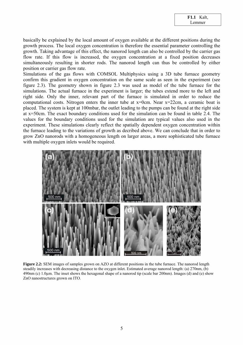
Experimental procedures The grown nanostructures were characterized by a LEO 1530 Gemini scanning electron microscope and an FEI Titan 80-300 high-resolution transmission electron microscope (in cooperation with CFN nanostructure service lab). For the latter, samples were prepared by mechanically scraping the nanorods from the substrate by a scalpel and dispersing them in high-purity ethanol. The nanorod/ethanol dispersion is ultrasonicated to minimize clustering of the nanorods. A small drop of the dispersion is then deposited on a circular copper grid covered by a thin holey carbon film. In order to simulate the oxygen gradient and gas flows inside the tube furnace, COMSOL Multiphysics (v3.5a) simulations were performed, coupling the non-isothermal flow, convection, and diffusion equations and using a 3D tube furnace geometry. Photoluminescence measurements were performed at 11 K in a cryostat. The 325 nm line of a HeCd-laser was used for excitation under an angle of incidence of 45°. The luminescence signal was dispersed by a spectrometer (1200 line/mm grating) and detected by a charged-coupled device (Andor iDus, L.O.T. Oriel Europe). Controlling the length of the nanorods The grown nanostructures were investigated by a scanning electron microscope (SEM). The nanorods grow almost perpendicular to the substrates, show a narrow length distribution on a centimeter lateral scale and exhibit a hexagonal morphology (see inset to figure 2.2c), indicating a growth along the c-axis [0001]. The series of figures 2.2a-c shows the dependence of the nanorod morphology on the position relative to the oxygen inlet within the tube. The length of the nanorods increases from sample to sample with decreasing distance (several tenths of a centimeter) to the oxygen inlet. The nanorod dimension ranges from 200 nm to several micrometers in length and from 40 nm to 1.2 µm in diameter. In order to understand this finding, the growth process is discussed in more detail in the following. During the preheating of the tube furnace, the nitrogen carrier gas flow is switched on, unlike the oxygen flow. When the source material has reached a certain temperature, zinc vapor is produced which is transported through the tube by the carrier gas flow. A thin zinc seed layer may form on the substrates by this vapor. No significant differences between the seed layers on the substrates placed at different positions in the tube is expected, as at this point the artificial air flow is not yet started and the tube furnace is uniformly heated. When the whole furnace has reached its final temperature, the artificial air flow is started, providing oxygen by the central inlet. The gradual increase of the nanorod dimension towards this inlet can thus
F1.1 Kalt, Lemmer
5
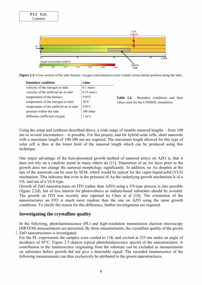
basically be explained by the local amount of oxygen available at the different positions during the growth process. The local oxygen concentration is therefore the essential parameter controlling the growth. Taking advantage of this effect, the nanorod length can also be controlled by the carrier gas flow rate. If this flow is increased, the oxygen concentration at a fixed position decreases simultaneously resulting in shorter rods. The nanorod length can thus be controlled by either position or carrier gas flow rate. Simulations of the gas flows with COMSOL Multiphysics using a 3D tube furnace geometry confirm this gradient in oxygen concentration on the same scale as seen in the experiment (see figure 2.3). The geometry shown in figure 2.3 was used as model of the tube furnace for the simulations. The actual furnace in the experiment is larger; the tubes extend more to the left and right side. Only the inner, relevant part of the furnace is simulated in order to reduce the computational costs. Nitrogen enters the inner tube at x=0cm. Near x=22cm, a ceramic boat is placed. The system is kept at 100mbar, the outlet leading to the pumps can be found at the right side at x=50cm. The exact boundary conditions used for the simulation can be found in table 2.4. The values for the boundary conditions used for the simulation are typical values also used in the experiment. These simulations clearly reflect the spatially dependent oxygen concentration within the furnace leading to the variations of growth as decribed above. We can conclude that in order to grow ZnO nanorods with a homogeneous length on larger areas, a more sophisticated tube furnace with multiple oxygen inlets would be required.
Figure 2.2: SEM images of samples grown on AZO at different positions in the tube furnace. The nanorod length steadily increases with decreasing distance to the oxygen inlet. Estimated average nanorod length: (a) 270nm, (b) 490nm (c) 1.0µm. The inset shows the hexagonal shape of a nanorod tip (scale bar 200nm). Images (d) and (e) show ZnO nanostructures grown on ITO.
F1.1 Kalt, Lemmer
6
Figure 2.3: Cross section of the tube furnace: oxygen concentration (color coded) versus lateral position along the tube. Table 2.4. Boundary conditions and their values used for the COMSOL simulation.
Using the setup and synthesis described above, a wide range of tunable nanorod lengths - from 100 nm to several micrometers – is possible. For this project, and for hybrid solar cells, short nanorods with a maximum length of 100-200 nm are required. The maximum length allowed for this type of solar cell is thus at the lower limit of the nanorod length which can be produced using this technique. One major advantage of the here-presented growth method of nanorod arrays on AZO is, that it does not rely on a catalytic metal as many others do [11]. Deposition of an Au layer prior to the growth does not change the nanorod morphology significantly. In addition, no Au droplets at the tips of the nanorods can be seen by SEM, which would be typical for the vapor-liquid-solid (VLS) mechanism. This indicates that even in the presence of Au the underlying growth mechanism is of a VS- and not of a VLS-type. Growth of ZnO nanostructures on ITO (rather than AZO) using a VS-type process is also possible (figure 2.2d), but of less interest for photovoltaics as indium-based substrates should be avoided. The growth on ITO was recently also reported by Chen et al [14]. The orientation of the nanostructures on ITO is much more random than the one on AZO using the same growth conditions. To clarify the reason for this difference, further investigations are required.
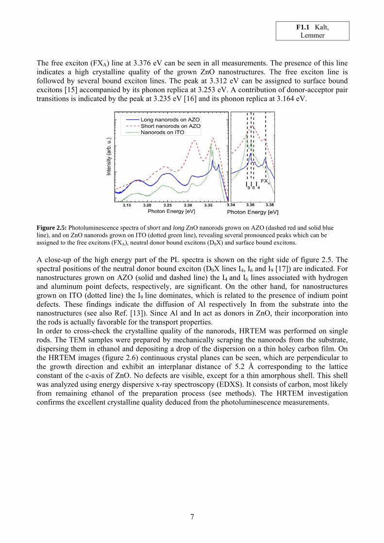
Investigating the crystalline quality In the following, photoluminescence (PL) and high-resolution transmission electron microscopy (HRTEM) measurements are presented. By these measurements, the crystalline quality of the grown ZnO nanostructures is investigated. For the PL experiments the samples were cooled to 11K and excited at 325 nm under an angle of incidence of 45°C. Figure 2.5 depicts typical photoluminescence spectra of the nanostructures. A contribution to the luminescence originating from the substrate can be excluded as measurements on substrates before growth did not give a detectable signal. The recorded luminescence of the following measurements can thus exclusively be attributed to the grown nanostructures.
boundary condition value
velocity of the nitrogen at inlet 0.1 mm/s velocity of the artificial air at inlet 0.15 mm/s
temperature of the furnace 510°C
temperature of the nitrogen at inlet 20°C
temperature of the artificial air at inlet 510°C
pressure within the tube 100 mbar
diffusion coefficient oxygen 1 m²/s
F1.1 Kalt, Lemmer
7
The free exciton (FXA) line at 3.376 eV can be seen in all measurements. The presence of this line indicates a high crystalline quality of the grown ZnO nanostructures. The free exciton line is followed by several bound exciton lines. The peak at 3.312 eV can be assigned to surface bound excitons [15] accompanied by its phonon replica at 3.253 eV. A contribution of donor-acceptor pair transitions is indicated by the peak at 3.235 eV [16] and its phonon replica at 3.164 eV.
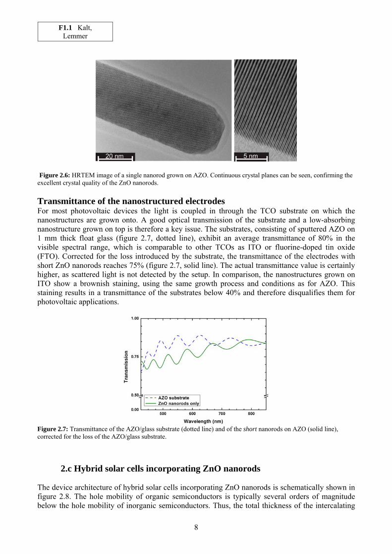
Figure 2.5: Photoluminescence spectra of short and long ZnO nanorods grown on AZO (dashed red and solid blue line), and on ZnO nanorods grown on ITO (dotted green line), revealing several pronounced peaks which can be assigned to the free excitons (FXA), neutral donor bound excitons (D0X) and surface bound excitons. A close-up of the high energy part of the PL spectra is shown on the right side of figure 2.5. The spectral positions of the neutral donor bound exciton (D0X lines I4, I6 and I9 [17]) are indicated. For nanostructures grown on AZO (solid and dashed line) the I4 and I6 lines associated with hydrogen and aluminum point defects, respectively, are significant. On the other hand, for nanostructures grown on ITO (dotted line) the I9 line dominates, which is related to the presence of indium point defects. These findings indicate the diffusion of Al respectively In from the substrate into the nanostructures (see also Ref. [13]). Since Al and In act as donors in ZnO, their incorporation into the rods is actually favorable for the transport properties. In order to cross-check the crystalline quality of the nanorods, HRTEM was performed on single rods. The TEM samples were prepared by mechanically scraping the nanorods from the substrate, dispersing them in ethanol and depositing a drop of the dispersion on a thin holey carbon film. On the HRTEM images (figure 2.6) continuous crystal planes can be seen, which are perpendicular to the growth direction and exhibit an interplanar distance of 5.2 Å corresponding to the lattice constant of the c-axis of ZnO. No defects are visible, except for a thin amorphous shell. This shell was analyzed using energy dispersive x-ray spectroscopy (EDXS). It consists of carbon, most likely from remaining ethanol of the preparation process (see methods). The HRTEM investigation confirms the excellent crystalline quality deduced from the photoluminescence measurements.
F1.1 Kalt, Lemmer
8
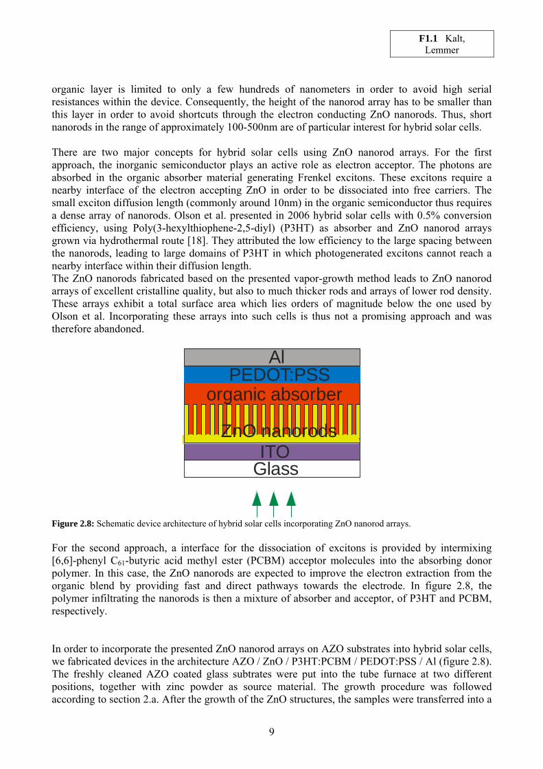
Figure 2.6: HRTEM image of a single nanorod grown on AZO. Continuous crystal planes can be seen, confirming the excellent crystal quality of the ZnO nanorods. Transmittance of the nanostructured electrodes For most photovoltaic devices the light is coupled in through the TCO substrate on which the nanostructures are grown onto. A good optical transmission of the substrate and a low-absorbing nanostructure grown on top is therefore a key issue. The substrates, consisting of sputtered AZO on 1 mm thick float glass (figure 2.7, dotted line), exhibit an average transmittance of 80% in the visible spectral range, which is comparable to other TCOs as ITO or fluorine-doped tin oxide (FTO). Corrected for the loss introduced by the substrate, the transmittance of the electrodes with short ZnO nanorods reaches 75% (figure 2.7, solid line). The actual transmittance value is certainly higher, as scattered light is not detected by the setup. In comparison, the nanostructures grown on ITO show a brownish staining, using the same growth process and conditions as for AZO. This staining results in a transmittance of the substrates below 40% and therefore disqualifies them for photovoltaic applications.
Figure 2.7: Transmittance of the AZO/glass substrate (dotted line) and of the short nanorods on AZO (solid line), corrected for the loss of the AZO/glass substrate.
2.c Hybrid solar cells incorporating ZnO nanorods The device architecture of hybrid solar cells incorporating ZnO nanorods is schematically shown in figure 2.8. The hole mobility of organic semiconductors is typically several orders of magnitude below the hole mobility of inorganic semiconductors. Thus, the total thickness of the intercalating
F1.1 Kalt, Lemmer
9
organic layer is limited to only a few hundreds of nanometers in order to avoid high serial resistances within the device. Consequently, the height of the nanorod array has to be smaller than this layer in order to avoid shortcuts through the electron conducting ZnO nanorods. Thus, short nanorods in the range of approximately 100-500nm are of particular interest for hybrid solar cells. There are two major concepts for hybrid solar cells using ZnO nanorod arrays. For the first approach, the inorganic semiconductor plays an active role as electron acceptor. The photons are absorbed in the organic absorber material generating Frenkel excitons. These excitons require a nearby interface of the electron accepting ZnO in order to be dissociated into free carriers. The small exciton diffusion length (commonly around 10nm) in the organic semiconductor thus requires a dense array of nanorods. Olson et al. presented in 2006 hybrid solar cells with 0.5% conversion efficiency, using Poly(3-hexylthiophene-2,5-diyl) (P3HT) as absorber and ZnO nanorod arrays grown via hydrothermal route [18]. They attributed the low efficiency to the large spacing between the nanorods, leading to large domains of P3HT in which photogenerated excitons cannot reach a nearby interface within their diffusion length. The ZnO nanorods fabricated based on the presented vapor-growth method leads to ZnO nanorod arrays of excellent cristalline quality, but also to much thicker rods and arrays of lower rod density. These arrays exhibit a total surface area which lies orders of magnitude below the one used by Olson et al. Incorporating these arrays into such cells is thus not a promising approach and was therefore abandoned.
ITOGlass
PEDOT:PSSAl
organic absorber
ZnO nanorods
Figure 2.8: Schematic device architecture of hybrid solar cells incorporating ZnO nanorod arrays. For the second approach, a interface for the dissociation of excitons is provided by intermixing [6,6]-phenyl C61-butyric acid methyl ester (PCBM) acceptor molecules into the absorbing donor polymer. In this case, the ZnO nanorods are expected to improve the electron extraction from the organic blend by providing fast and direct pathways towards the electrode. In figure 2.8, the polymer infiltrating the nanorods is then a mixture of absorber and acceptor, of P3HT and PCBM, respectively. In order to incorporate the presented ZnO nanorod arrays on AZO substrates into hybrid solar cells, we fabricated devices in the architecture AZO / ZnO / P3HT:PCBM / PEDOT:PSS / Al (figure 2.8). The freshly cleaned AZO coated glass subtrates were put into the tube furnace at two different positions, together with zinc powder as source material. The growth procedure was followed according to section 2.a. After the growth of the ZnO structures, the samples were transferred into a
F1.1 Kalt, Lemmer
10
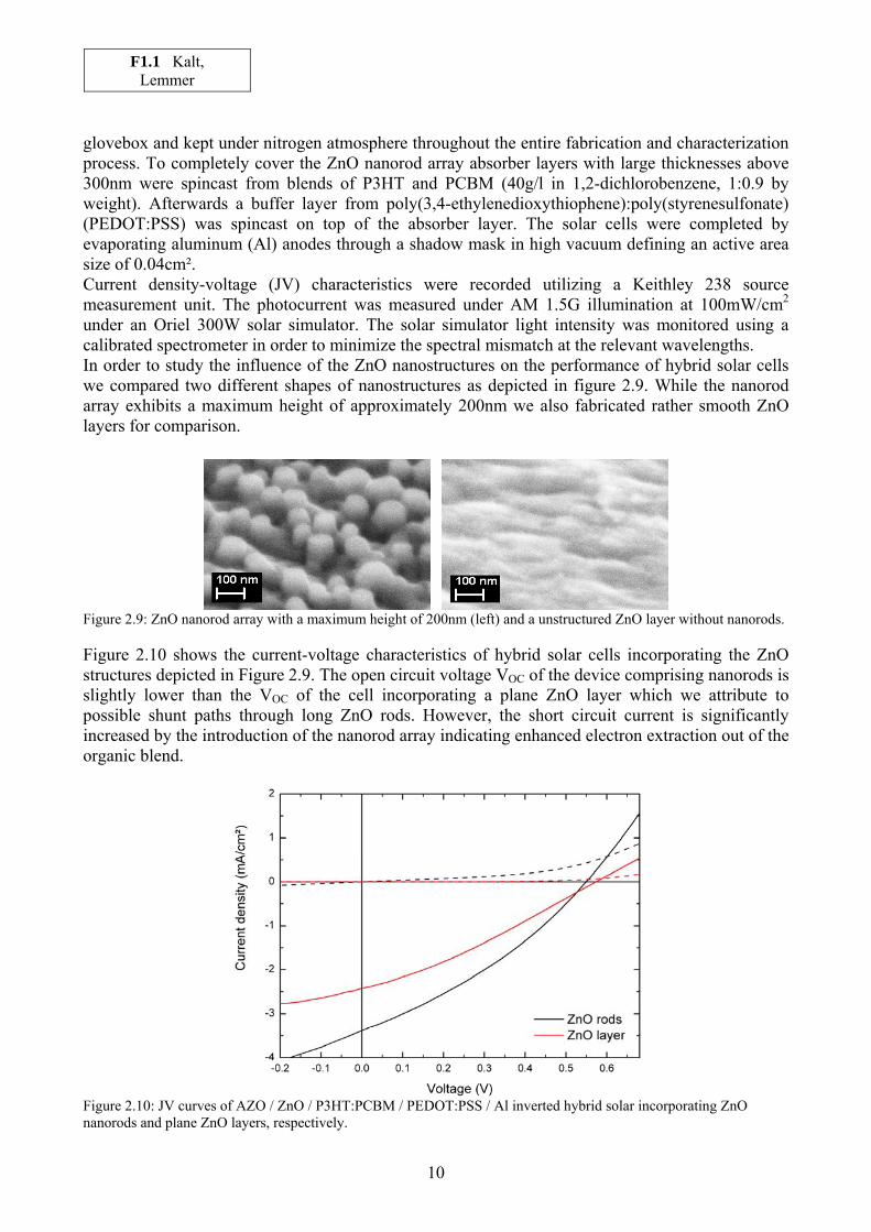
glovebox and kept under nitrogen atmosphere throughout the entire fabrication and characterization process. To completely cover the ZnO nanorod array absorber layers with large thicknesses above 300nm were spincast from blends of P3HT and PCBM (40g/l in 1,2-dichlorobenzene, 1:0.9 by weight). Afterwards a buffer layer from poly(3,4-ethylenedioxythiophene):poly(styrenesulfonate) (PEDOT:PSS) was spincast on top of the absorber layer. The solar cells were completed by evaporating aluminum (Al) anodes through a shadow mask in high vacuum defining an active area size of 0.04cm². Current density-voltage (JV) characteristics were recorded utilizing a Keithley 238 source measurement unit. The photocurrent was measured under AM 1.5G illumination at 100mW/cm2 under an Oriel 300W solar simulator. The solar simulator light intensity was monitored using a calibrated spectrometer in order to minimize the spectral mismatch at the relevant wavelengths. In order to study the influence of the ZnO nanostructures on the performance of hybrid solar cells we compared two different shapes of nanostructures as depicted in figure 2.9. While the nanorod array exhibits a maximum height of approximately 200nm we also fabricated rather smooth ZnO layers for comparison.
Figure 2.9: ZnO nanorod array with a maximum height of 200nm (left) and a unstructured ZnO layer without nanorods. Figure 2.10 shows the current-voltage characteristics of hybrid solar cells incorporating the ZnO structures depicted in Figure 2.9. The open circuit voltage VOC of the device comprising nanorods is slightly lower than the VOC of the cell incorporating a plane ZnO layer which we attribute to possible shunt paths through long ZnO rods. However, the short circuit current is significantly increased by the introduction of the nanorod array indicating enhanced electron extraction out of the organic blend.
Figure 2.10: JV curves of AZO / ZnO / P3HT:PCBM / PEDOT:PSS / Al inverted hybrid solar incorporating ZnO nanorods and plane ZnO layers, respectively.
F1.1 Kalt, Lemmer
11
However, due to the increased absorber layer thickness and thus rising serial resistance of the devices, the overall energy conversion efficiency of 0.6% is quite poor as compared to state-of-the-art P3HT:PCBM solar cells. In order to fabricate highly efficient solar cells, the height of the nanorods has thus to be significantly decreased. In addition, another detrimental property of the ZnO arrays is the low density of the rods (number of rods per µm²) as compared to arrays grown via hydrothermal routes. Using the presented vapor growth method these requirements can hardly be met as there are only few parameters to manipulate the self-assembling growth process of the ZnO nanorods. We may therefore conclude that though we have shown that tailored ZnO nanostructures can enhance the performance of hybrid solar cells, the VS growth mechanism is not suitable for fabricating high-density arrays with a smaller height which we regard as inevitable for further experiments.
2.d Conclusion
In conclusion to this section, we presented a growth method and characterization of ZnO nanorod arrays which exhibit excellent crystalline quality and which are tunable in length (within limitations). However, these arrays are not suitable for efficient hybrid solar cells, as the nanorod dimension and density match only unsatisfactorily the requirements for this type of solar cell. Denser arrays with rods of smaller diameter and length are required, but cannot be fabricated using our growth method. For this reason, despite a superior crystalline quality compared to hydrothermal approaches, the presented ZnO nanorod arrays do not improve significantly the device efficiency.
3. Indium-doped ZnO nanoparticles In this section, the synthesis of the IZO nanoparticles and the preparation steps of the photovoltaic devices is presented (3.a). In the following chapters the characterization of inverted single devices (3.b) and of tandem devices (3.c) is presented.
3.a Experimental/Synthesis
IZO nanoparticles were synthesized in liquid phase using a microwave-assisted polyol synthesis as developed within CFN project F1.3 and published by E. Hammarberg et al. [19]. In a typical recipe, 4.56 mmol of Zn(CH3COO)2 2 H2O and 0.23 mmol of InCl3 4 H2O were dissolved in 50 ml DEG. Subsequently, 1 ml deionized H2O was added. As the solution was heated to 200 °C in a standard laboratory microwave oven (MLS rotaprep: 1200 W, 2.45 GHz; fiber optic as well as pyrometer for temperature control; magnetic stirrer), precipitation was observed. To improve material crystallinity, the temperature was maintained for 30 min. During irradiation, the sample was continuously stirred and vented with argon. As-prepared IZO suspensions with 5 mol-% indium-doping were colloidally stable for months. They exhibit a transparent appearance and a slight bluish shade. After the microwave-assisted polyol-synthesis, the resulting suspensions were separated by centrifugation and washed three times by redispersion in and centrifugation from
F1.1 Kalt, Lemmer
12
ethanol. In order to allow a fast deposition process for the fabrication of hybrid solar cells the slightly bluish powders were finally redispersed in the low boiling point solvent ethanol. For inverted single junction solar cells we utilized an ITO / IZO / P3HT:PCBM / PEDOT:PSS / Al architecture. Tandem solar cells were fabricated with an ITO / IZO / P3HT:PCBM / PEDOT:PSS / IZO / P3HT:PCBM / PEDOT:PSS / Al layer sequence. For the solar cell fabrication ITO coated glass was structured and cleaned under ultrasonication. Then the substrates were exposed to an oxygen plasma to remove organic remnants. After cleaning, the substrates were transferred into a glovebox and kept under nitrogen atmosphere throughout the entire fabrication and characterization process. Nanoparticles (1 wt-% in ethanol), the P3HT:PCBM blend and PEDOT:PSS were deposited using spin coating techniques while the aluminum counter electrode was deposited in high vacuum through a shadow mask. The current-density-voltage (J-V) characteristics were measured using a Keithley 238 source measurement unit. Film thicknesses were determined using a Dektak 8000 profiler under ambient atmosphere.
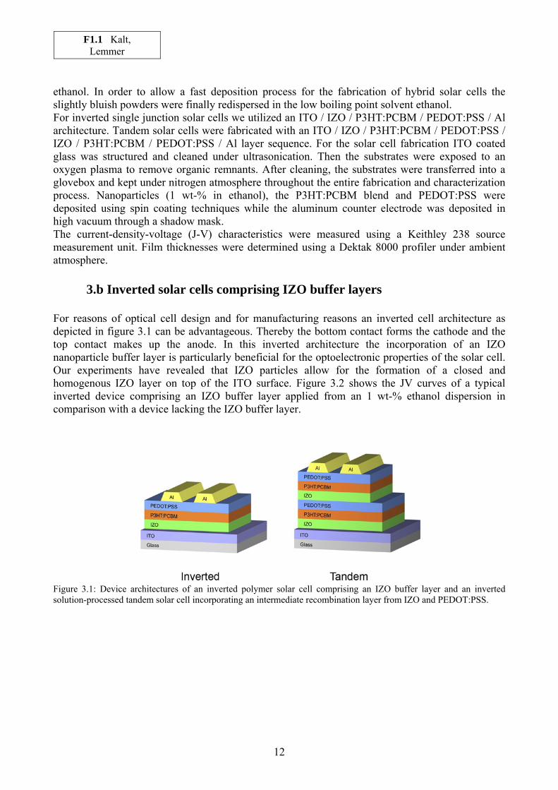
3.b Inverted solar cells comprising IZO buffer layers For reasons of optical cell design and for manufacturing reasons an inverted cell architecture as depicted in figure 3.1 can be advantageous. Thereby the bottom contact forms the cathode and the top contact makes up the anode. In this inverted architecture the incorporation of an IZO nanoparticle buffer layer is particularly beneficial for the optoelectronic properties of the solar cell. Our experiments have revealed that IZO particles allow for the formation of a closed and homogenous IZO layer on top of the ITO surface. Figure 3.2 shows the JV curves of a typical inverted device comprising an IZO buffer layer applied from an 1 wt-% ethanol dispersion in comparison with a device lacking the IZO buffer layer.
Figure 3.1: Device architectures of an inverted polymer solar cell comprising an IZO buffer layer and an inverted solution-processed tandem solar cell incorporating an intermediate recombination layer from IZO and PEDOT:PSS.
F1.1 Kalt, Lemmer
13
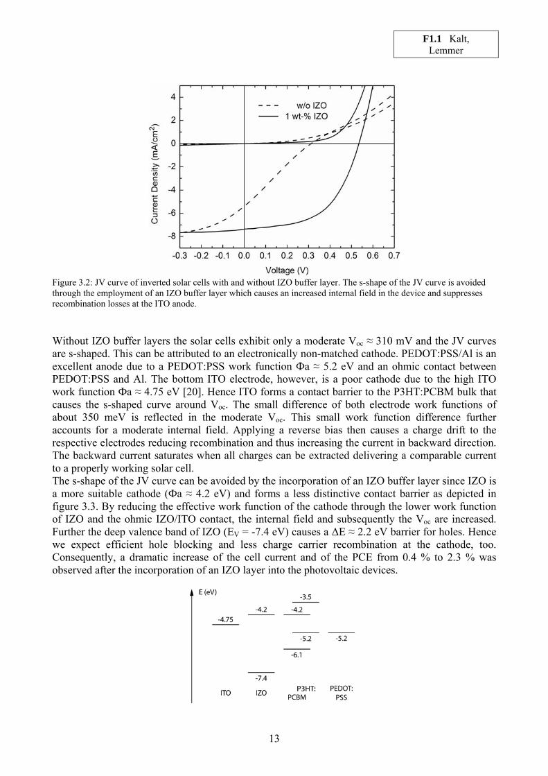
Figure 3.2: JV curve of inverted solar cells with and without IZO buffer layer. The s-shape of the JV curve is avoided through the employment of an IZO buffer layer which causes an increased internal field in the device and suppresses recombination losses at the ITO anode.
Without IZO buffer layers the solar cells exhibit only a moderate Voc ≈ 310 mV and the JV curves are s-shaped. This can be attributed to an electronically non-matched cathode. PEDOT:PSS/Al is an excellent anode due to a PEDOT:PSS work function Фa ≈ 5.2 eV and an ohmic contact between PEDOT:PSS and Al. The bottom ITO electrode, however, is a poor cathode due to the high ITO work function Фa ≈ 4.75 eV [20]. Hence ITO forms a contact barrier to the P3HT:PCBM bulk that causes the s-shaped curve around Voc. The small difference of both electrode work functions of about 350 meV is reflected in the moderate Voc. This small work function difference further accounts for a moderate internal field. Applying a reverse bias then causes a charge drift to the respective electrodes reducing recombination and thus increasing the current in backward direction. The backward current saturates when all charges can be extracted delivering a comparable current to a properly working solar cell. The s-shape of the JV curve can be avoided by the incorporation of an IZO buffer layer since IZO is a more suitable cathode (Фa ≈ 4.2 eV) and forms a less distinctive contact barrier as depicted in figure 3.3. By reducing the effective work function of the cathode through the lower work function of IZO and the ohmic IZO/ITO contact, the internal field and subsequently the Voc are increased. Further the deep valence band of IZO (EV = -7.4 eV) causes a ΔE ≈ 2.2 eV barrier for holes. Hence we expect efficient hole blocking and less charge carrier recombination at the cathode, too. Consequently, a dramatic increase of the cell current and of the PCE from 0.4 % to 2.3 % was observed after the incorporation of an IZO layer into the photovoltaic devices.
F1.1 Kalt, Lemmer
14
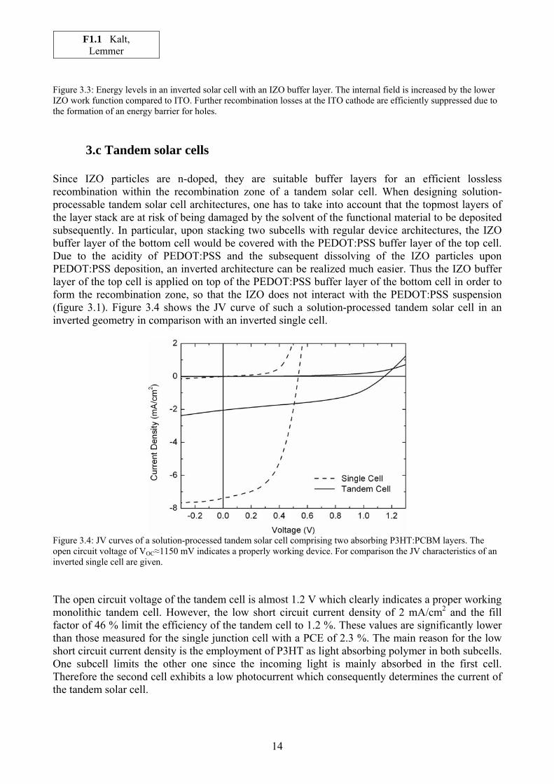
Figure 3.3: Energy levels in an inverted solar cell with an IZO buffer layer. The internal field is increased by the lower IZO work function compared to ITO. Further recombination losses at the ITO cathode are efficiently suppressed due to the formation of an energy barrier for holes.
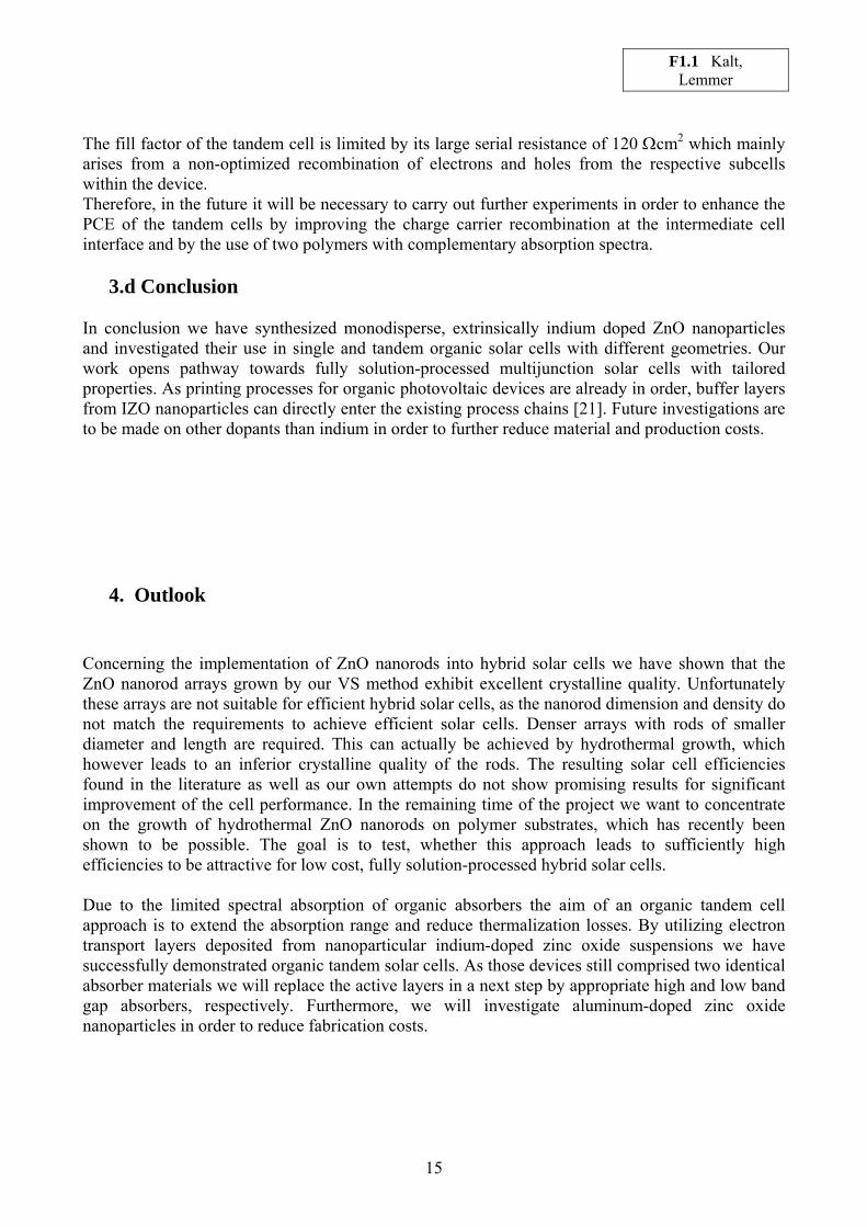
3.c Tandem solar cells Since IZO particles are n-doped, they are suitable buffer layers for an efficient lossless recombination within the recombination zone of a tandem solar cell. When designing solution-processable tandem solar cell architectures, one has to take into account that the topmost layers of the layer stack are at risk of being damaged by the solvent of the functional material to be deposited subsequently. In particular, upon stacking two subcells with regular device architectures, the IZO buffer layer of the bottom cell would be covered with the PEDOT:PSS buffer layer of the top cell. Due to the acidity of PEDOT:PSS and the subsequent dissolving of the IZO particles upon PEDOT:PSS deposition, an inverted architecture can be realized much easier. Thus the IZO buffer layer of the top cell is applied on top of the PEDOT:PSS buffer layer of the bottom cell in order to form the recombination zone, so that the IZO does not interact with the PEDOT:PSS suspension (figure 3.1). Figure 3.4 shows the JV curve of such a solution-processed tandem solar cell in an inverted geometry in comparison with an inverted single cell.
Figure 3.4: JV curves of a solution-processed tandem solar cell comprising two absorbing P3HT:PCBM layers. The open circuit voltage of VOC≈1150 mV indicates a properly working device. For comparison the JV characteristics of an inverted single cell are given.
The open circuit voltage of the tandem cell is almost 1.2 V which clearly indicates a proper working monolithic tandem cell. However, the low short circuit current density of 2 mA/cm2 and the fill factor of 46 % limit the efficiency of the tandem cell to 1.2 %. These values are significantly lower than those measured for the single junction cell with a PCE of 2.3 %. The main reason for the low short circuit current density is the employment of P3HT as light absorbing polymer in both subcells. One subcell limits the other one since the incoming light is mainly absorbed in the first cell. Therefore the second cell exhibits a low photocurrent which consequently determines the current of the tandem solar cell.
F1.1 Kalt, Lemmer
15
The fill factor of the tandem cell is limited by its large serial resistance of 120 cm2 which mainly arises from a non-optimized recombination of electrons and holes from the respective subcells within the device. Therefore, in the future it will be necessary to carry out further experiments in order to enhance the PCE of the tandem cells by improving the charge carrier recombination at the intermediate cell interface and by the use of two polymers with complementary absorption spectra.
3.d Conclusion In conclusion we have synthesized monodisperse, extrinsically indium doped ZnO nanoparticles and investigated their use in single and tandem organic solar cells with different geometries. Our work opens pathway towards fully solution-processed multijunction solar cells with tailored properties. As printing processes for organic photovoltaic devices are already in order, buffer layers from IZO nanoparticles can directly enter the existing process chains [21]. Future investigations are to be made on other dopants than indium in order to further reduce material and production costs.
4. Outlook Concerning the implementation of ZnO nanorods into hybrid solar cells we have shown that the ZnO nanorod arrays grown by our VS method exhibit excellent crystalline quality. Unfortunately these arrays are not suitable for efficient hybrid solar cells, as the nanorod dimension and density do not match the requirements to achieve efficient solar cells. Denser arrays with rods of smaller diameter and length are required. This can actually be achieved by hydrothermal growth, which however leads to an inferior crystalline quality of the rods. The resulting solar cell efficiencies found in the literature as well as our own attempts do not show promising results for significant improvement of the cell performance. In the remaining time of the project we want to concentrate on the growth of hydrothermal ZnO nanorods on polymer substrates, which has recently been shown to be possible. The goal is to test, whether this approach leads to sufficiently high efficiencies to be attractive for low cost, fully solution-processed hybrid solar cells. Due to the limited spectral absorption of organic absorbers the aim of an organic tandem cell approach is to extend the absorption range and reduce thermalization losses. By utilizing electron transport layers deposited from nanoparticular indium-doped zinc oxide suspensions we have successfully demonstrated organic tandem solar cells. As those devices still comprised two identical absorber materials we will replace the active layers in a next step by appropriate high and low band gap absorbers, respectively. Furthermore, we will investigate aluminum-doped zinc oxide nanoparticles in order to reduce fabrication costs.

F1.1 Kalt, Lemmer
16
References [1] N.S. Sariciftci, L. Smilowitz, A.J. Heeger, F. Wudl, Science, 1992, 258, 1474. [2] B. Maennig, J. Drechsel, D. Gebeyehu, P. Simon, F. Kozlowski, A. Werner, F. Li, S. Grundmann, S. Sonntag and M. Koch, et al., Appl. Phys. A, 2004, 79, 1. [3] L. Groenendaal, F. Jonas, D. Freitag, H. Pielartzik, J.R. Reynolds, Adv. Mater., 2000, 12, 481. [4] S. Bhadraa, D. Khastgir, N.K. Singha, J.H. Lee, Progress in Polymer Science, 2009, 34, 783. [5] J.Y. Kim, S.H. Kim, H.-H. Lee, K. Lee, W. Ma, X. Gong, A.J. Heeger, Adv. Mater., 2006, 18, 572. [6] M.S. White, D.C. Olson, S.E. Shaheen, N. Kopidakis, D.S. Ginley, Appl. Phys. Lett., 2006, 89, 143517. [7] H. Zhou, J. Fallert, J. Sartor, R.J.B. Dietz, C. Klingshirn, H. Kalt, D. Weissenberger, D. Gerthsen, H. Zeng, W. Cai, Ordered n-type ZnO nanorod arrays, Appl. Phys. Lett., 2008, 92, 132112. [8] H.J.Zhou, M.Wissinger, J.Fallert, R.Hauschild, F.Stelzl, C.Klingshirn, H.Kalt, Ordered, uniform-sized ZnO nanolaser arrays, Appl. Phys. Lett. 91, 181112 (2007) [9] W. Ma, C. Yang, X. Gong, K. Lee, A.J. Heeger, Adv. Funct. Mater., 2005, 15, 1617. [10] G. Li, V. Shrotriya, J. Huang., Y. Yao, T. Moriarty, K. Emery, Y. Yang, Nat. Mater., 2005, 4, 864. [11] P. Yang, H. Yan, S. Mao, R. Russo, J. Johnson, R. Saykally, N. Morris, J. Pham, R. He, H.-J. Choi, Adv. Func. Mat., 2002, 12, 323. [12] L.E. Greene, M. Law, D.H. Tan, M. Montano, J. Goldberger, G. Somorjai, P. Yang, Nano Letters, 2005, 5, 1231. [14] L.-Y. Chen, S.-H. Wu, Y.-T. Yin, J. Phys. Chem. C, 2009, 113, 21572. [15] J. Fallert, R. Hauschild, F. Stelzl, A. Urban, M. Wissinger, H. Zhou, C. Klingshirn, H. Kalt, Surface-state related luminescence in ZnO nanocrystals, J. Appl. Phys., 2007, 101, 073506. [16] A. Zeuner, H. Alves, D. Hofmann, B. Meyer, A. Hoffmann, U. Haboeck, M. Strassburg, M. Dworzak, Phys. Stat. Sol. B, 2002, 234, R7. [17] B.K. Meyer, H. Alves, D.M. Hofmann, W. Kriegseis, D. Forster, F. Bertram, J. Christen, A. Hoffmann, M. Straßburg, M. Dworzak, U. Haboeck, A.V. Rodina, Phys. Stat. Sol. B, 2004, 241, 231 [18] D.C. Olson, J. Piris, R.T. Collins, S.E. Shaheen, D.S. Ginley, Thin Solid Films, 2006, 496, 26. [19] E. Hammarberg, A. Prodi-Schwab, C. Feldmann, J. Coll. and Interf. Sci., 2009, 334, 29. [20] K. Sugiyama, H. Ishii, Y. Ouchi, K. Seki, J. Appl. Phys., 2000, 87, 295. [21] F. C. Krebs, T. Tromholt, M. Jørgensen, Nanoscale, 2010, 2, 873.


![[Pidruchniki.net] histukr zno 2015](https://img.pdfslide.org/doc/110x75/587a3c541a28abdb1c8b71fb/pidruchnikinet-histukr-zno-2015.jpg)