Embed Size (px)
Citation preview
Study of Surface Modified Silicon Nanoparticles for
Printable Optoelectronics
Von der Fakultät für Ingenieurwissenschaften, Abteilung Maschinenbau und
Verfahrenstechnik der
Universität Duisburg-Essen
zur Erlangung des akademischen Grades
DOKTOR-INGENIEUR
genehmigte Dissertation
von
Anoop Gupta
aus
Kanpur, India
Gutachter: Prof. Dr. rer.-nat. Christof Schulz/ Prof. Dr. Uwe Kortshagen
Tag der mündlichen Prüfung: 27.06.2011


Dedicated to the research community
The process of scientific discovery is, in effect, a continual flight from wonder.
- Albert Einstein

�
Acknowledgements
Four years ago, I started a journey in the fascinating and colorful world of nano silicon. It was
the most memorable and exciting endeavor in my research career. This journey would not have
been possible without the support of my supervisors, Prof. Christof Schulz and Dr. Hartmut
Wiggers. I would like to give my sincere thanks to them for providing me the chance to do a
Ph.D in their research group. Their contribution is invaluable. They assist me in all possible ways
to mature myself not only scientifically but also professionally. They always encouraged me to
present my work in various conferences around the world and to do collaborative research with
other groups. These opportunities helped me to understand the current state-of-the-art and
availed me with technical advances.
When I started, I knew almost nothing about silicon nanoparticles. At that time if some-
one asked me “why silicon nanoparticles are interesting”: I could only answer- because it will
give me a Ph.D degree. Well, in order to avoid this answer, I started to learn about it from papers
and books. Also, I started to collaborate and discuss with people to learn from their experience
and generate new ideas. I give my special thanks to Prof. Mark T. Swihart (University at Buffalo,
USA) for giving me an opportunity to work in his research group for two months. I gained a lot
of hands-on experience on silicon nanoparticles while working there. I am thankful to Prof. Mar-
kus Winterer, Prof. Axel Lorke and Prof. Michael Farle in our university for allowing me to do
the characterization of particles in their labs. I also thank Prof. Carola Kryschi (Friedrich-
Alexander-University Erlangen, Germany) and Prof. Ulrich Simon (RWTH Aachen University,
Germany) for giving me an opportunity to do some experiments in their labs.
Although four years have passed, I still feel that it was just yesterday when I started my
Ph.D. That is because I had such a great time with my wonderful colleagues and friends in Duis-
burg. Sonja- It was really fun doing crazy things like taking funny pictures and celebrating April
fool with you. You tried to teach me German but finally you learned Hindi �. Ashrina, Helge,
Nils and Malin– It was great listening your stories about “Tiger”. Ali- Thanks for being so kind

and helping me with everything (writing letters in German, solving computer problems….well, it
is a long list �). Khadijeh- Thanks for being so nice and helpful. It still makes me smile when I
remember my discussion with you and Ali about “How evolution will change humans in future”.
Ruzica- You are the person, whom I always see first in a conference. Thanks for being so recog-
nizable. I never felt that I went to a wrong venue �. Oliver- It was really great to discuss with
you about everything under (and in) the sky. Alessandro- Thanks for showing me beautiful Ve-
nice and the traditional graduate ceremony in your formal university. Robert- I can´t forget our
funny and innovative discussion about the “Ink-jet printing technology” that we had after the
workshop in Erlangen. Sebastian- It was a nice experience to supervise your bachelor thesis.
Hans- Thanks for helping me with the Glove box connection. Ingo- Thanks for being so friendly
and always helpful. Pascal- Thanks for teaching me synthesis and helping me to buy stuffs for
my apartment. Barbara (Graft) and Barbara (Nota) �- Thanks for helping me with all the admin-
istrative work. Natascha and Beate- Thanks for being so nice and helpful with every little thing.
Dieter- Thanks for all your lab security seminars and uploading the TEM video. Tim- Thanks for
giving the memorable ride from Boston to New York. Ahmed- It was nice to crack jokes with
you, Oliver and Alessandro after our lunch breaks. Klemens- Thank you for leaving your plasma
reactor for us. Beril (aka Berelium)- It was really great (also tiring �) to do TEM of your series
of samples. I still have those funny pictures of nanoparticles, which were nano but not nanopar-
ticles.
There were also other people outside my group who directly or indirectly contributed in
my research. I am thankful to Ralf and Marina (for helping with HR-TEM), Andreas (for teach-
ing me FTIR), Jens and Matthias (for helping with PL measurement), Ryan (for proving QY da-
ta), Horst (for teaching me TEM), Andre (for providing EPR data) and Folarin (for helping me
with my experiments at the University at Buffalo).
Worth mentioning names of my friends, Moazzam and Rehan for all those chilled and re-
laxed evenings. It was fun to discuss our special topics without ever reaching any conclusions.
Gautam- Thanks for pushing me to think a short title for my thesis and all the useful discussions
we had. Sanjeev- I thank you for motivating me when I was struggling in the lab with my expe-
riments. Sanjubala- Thanks for tolerating us for never ending discussions on physics in your of-
fice. Erdal- Thanks for being so helpful with everything. Kartik- Thanks for your help in patient-
ly reading and editing my thesis. Martin- Thanks for helping me to improve my German.

Though, it was always hectic and we could barely manage to practice it. Ahmed Khalil- It was
great to work with you in collaboration. I remember those days in Hongkong when we were des-
perately searching for palatable food. Udo- I always took a chance to pass by your office to see
your cheerful face.
Deepti- I really enjoyed your wonderful surprises on my birthdays. Reeta- Thanks for
pushing me so hard with my thesis writing and taking some time to read it. It was always fun to
argue with you on “Animal Conservation” topic �. Mummy and Papa- Thanks for all your con-
stant support and encouragements. Swati and Arun- Thank you for your affection and support.
Sangeeta- Thanks for all the funny and relaxing conversations. I hope one day you will be able to
convince me to give you a Solitaire.
Hartmut, Ingo and Sonja- Thank you for coming to India to attend my marriage. It is a
wonderful memory that we will always cherish �.
Last but not least, I would like to thank silicon nanoparticles for allowing me to explore
some of their behavior �.
“Nanoparticles are really smart”- I lived four years with silicon nanoparticles but I still did not understand them. It’s still a long way to go……
Table of contents �
1� Introduction ............................................................................................................................. 1�
2� State of the art ......................................................................................................................... 4�
3� Methodologies......................................................................................................................... 9�
3.1� Synthesis........................................................................................................................... 9�
3.1.1� Microwave plasma synthesis of Si-NPs .................................................................... 9�
3.1.1.1� Background ........................................................................................................ 9�
3.1.1.2� Experimental details ........................................................................................ 11�
3.1.2� Etching of Si-NPs ................................................................................................... 11�
3.1.2.1� Background ...................................................................................................... 11�
3.1.2.2� Experimental details ........................................................................................ 14�
3.1.3� Surface functionalization of Si-NPs ........................................................................ 14�
3.1.3.1� Background ...................................................................................................... 14�
3.1.3.2� Experimental details ........................................................................................ 16�
3.1.4� Ink-jet printing of Si-NPs........................................................................................ 17�
3.1.4.1� Background ...................................................................................................... 17�
3.1.4.2� Experimental details ........................................................................................ 18�
3.2� Characterization ............................................................................................................. 19�
3.2.1� X-ray diffraction (XRD) ......................................................................................... 19�
3.2.1.1� Background ...................................................................................................... 19�
3.2.1.2� Experimental details ........................................................................................ 21
3.2.2� Transmission electron microscopy (TEM) ............................................................. 21�
3.2.2.1� Background ...................................................................................................... 21�
3.2.2.2� Experimental details ........................................................................................ 23�
3.2.3� Impedance spectroscopy (IS) .................................................................................. 23�
3.2.3.1� Background ...................................................................................................... 23�
3.2.3.2� Experimental details ........................................................................................ 24�
3.2.4� Fourier transform infrared (FTIR) spectroscopy .................................................... 25�
3.2.4.1� Background ...................................................................................................... 25�
3.2.4.2� Experimental details ........................................................................................ 28�
3.2.5� Electron paramagnetic resonance (EPR) spectroscopy ........................................... 28�
3.2.5.1� Background ...................................................................................................... 28�
3.2.5.2� Experimental details ........................................................................................ 30�
3.2.6� Photoluminescence (PL) spectroscopy ................................................................... 31�
3.2.6.1� Background ...................................................................................................... 31�
3.2.6.2� Experimental details ........................................................................................ 32�
3.2.7� Photoluminescence quantum yield (QY) ................................................................ 32�
3.2.7.1� Background ...................................................................................................... 32�
3.2.7.2� Experimental details ........................................................................................ 33�
4� Results and discussion .......................................................................................................... 34�
4.1� Synthesis and surface modification of Si-NPs ............................................................... 34�
4.1.1� Synthesis of Si-NPs................................................................................................. 34�
4.1.2� Etching of Si-NPs ................................................................................................... 40�
4.1.3� Surface functionalization of Si-NPs ........................................................................ 42
4.2� Optical properties of Si-NPs .......................................................................................... 48�
4.2.1� Optical properties of etched Si-NPs ........................................................................ 48�
4.2.1.1� Influence of etching with HF ........................................................................... 48�
4.2.1.2� Influence of etching with HF and HNO3 ......................................................... 51�
4.2.1.3� Air stability of etched Si-NPs .......................................................................... 54�
4.2.2� Optical properties of functionalized Si-NPs ........................................................... 57�
4.2.2.1� Influence of surface functionalization ............................................................. 57�
4.2.2.2� Factors influencing the PL properties of functionalized Si-NPs ..................... 59�
4.2.2.3� Air stability of functionalized Si-NPs ............................................................. 64�
4.2.2.4� Quantum yield of functionalized Si-NPs ......................................................... 69�
4.3� Electrical properties of Si-NPs ....................................................................................... 71�
4.3.1� Influence of etching and surface re-oxidation ........................................................ 73�
4.3.2� Influence of surface functionalization .................................................................... 75�
4.4� Dispersion stability and ink-jet printing of Si-NPs ........................................................ 80�
4.4.1� Stability of Si-NPs dispersion ................................................................................. 80�
4.4.2� Printing of functionalized Si-NPs ........................................................................... 82�
4.5� Synthesis of cross-linked Si-NPs network ..................................................................... 87�
5� Summary and conclusions .................................................................................................... 93�
6� Recommendations for future work ....................................................................................... 97�
7� References ............................................................................................................................. 99�
8� Appendix A ......................................................................................................................... 111�
List of own publications.............................................................................................................. 120�
Curriculum vitae ......................................................................................................................... 124�

List of symbols, abbreviations and acronyms
Latin symbols
a Lattice parameter
A Absorbance
A0 Baseline to peak area of the reference sample
A1 Baseline to peak area of the hydrosilylated sample
Ac Cross section area of the pellet
ASiHn Baseline to peak area of SiHn absorption
ASiOSi Baseline to peak area of SiOSi absorption
B Magnetic field strength
c Speed of light
dhkl Interplanar distance
dp Mean particle diameter
dNP Nanoparticle diameter
e Electronic charge
E Energy
E0 Band gap of bulk silicon
Ea Activation energy
Eg Band gap
ED Activation energy for diffusion

EF Functionalization efficiency
EPL Energy position at the maximum photoluminescence intensity
E� Energy of electron in a parallel alignment
E� Energy of electron in an antiparallel alignment
fosc Oscillator strength
F(�) Fourier transformation function
g Spectroscopic splitting factor
h Planck’s constant
I Transmitted intensity
Io Incident intensity
I(�) Spectral irradiation
k Reaction constant
k0 Pre-exponential factor
kb Boltzmann constant
K Absorption modulus
L Crystallite size
mo Rest mass of the electron
ms Magnetic quantum number
n Integer number
N Number density of particles
Np Number density of precursor molecules
N� Number of electrons with � spins
N� Number of electrons with � spins
p Partial pressure of primary growth species (monomers)

ps Equilibrium vapor pressure
r Radius of cluster
rth Resolution limit
r* Radius of critical cluster
R Universal gas constant
Rt Total resistance
R� Degree of reflection
s Spin quantum number
S Scattering modulus
So Oxidation susceptibility index
t Time
tet Etching time
T Temperature
T Transmittance
Tp Thickness of the pellet
U Accelerating voltage
Vm Molar volume
Z Total impedance
Z´ Real part of total impedance
Z´´ Imaginary part of total impedance
Greek symbols
�E�-� Energy difference between � and � spin of electron
�E Spectral width

� Specific conductivity
� Surface energy
�o Specific conductivity at temperature 0K
�g Geometric standard deviation
�T Specific conductivity at temperature T
� Full width at half maximum
�c Collision frequency function
�c Characteristic time for coagulation
�s Characteristic time for coalescence
Incident angle
Frequency
~ Wavenumber
� Wavelength
� Angular frequency
�B Bohr magneton
Abbreviations and acronyms
BP Boiling point
BF Bright field
D-centers Dangling bonds in a disordered environment
DF Dark field
EMP Ethyl-2-methyl-4-pentenoate
EPR Electron paramagnetic resonance
ETU Ethyl undecylenate

FFT Fast Fourier transformation
FTIR Fourier transform infrared
FWHM Full width at half maximum
HR-TEM High resolution transmission electron microscope
IS Impedance spectroscopy
LED Light emitting diode
NMR Nuclear magnetic resonance
Pb-center Trivalent silicon atoms located at the Si/SiOx interface
PL Photoluminescence
PVDF Polyvinylidene fluoride
QY Quantum yield
SIMS Secondary ion mass spectroscopy
STM Scanning tunneling microscopy
TEM Transmission electron microscope
TMR Tunneling magnetoresistance
UV Ultraviolet
VB Vinyl benzoate
XRD X-ray diffraction
1
1 Introduction
Nanoparticles, which are commonly defined as particles below 100 nm, are the fundamental
building blocks of most nanomaterial based devices. Properties of bulk materials are typically
constant as a function of size, however, nanomaterials exhibit size dependent physical, chemical,
magnetic, electrical and optical properties [1, 2]. Nanomaterials have the potential to profoundly
change our economy and to improve our standard of living. Most computer hard drives, for in-
stance, contain giant tunneling magnetoresistance (TMR) heads that, through nano-thin layers of
magnetic materials, allow a significant increase in the storage capacity [3, 4]. The use of nano-
structure electrode in the lithium ion battery increases its energy capacity compared to conven-
tional lithium ion batteries [5]. Coatings based on titanium dioxide nanoparticles have self clean-
ing properties [6]. High-power and high-energy storage capacitors can be designed by use of
nanostructured carbon as electrode materials [7]. Numerous products featuring unique properties
of nanoscale materials are already available in market. According to ScienceDaily [8], new
products based on nanomaterials are entering into the market at the rate of 3–4 per week.
Silicon has been a material of great scientific and commercial interest for decades be-
cause of its high availability, cost effectiveness, biocompatibility, and compatibility with the
well-established silicon-microelectronics technology. High-purity silicon is used in a variety of
electronic devices, ranging from computer microchips, transistors, liquid-crystal displays, and
semiconductor-based detectors. According to the US Geological Survey, the world’s reserves of
silicon exceeded five million tons in 2007 — the best indicator of its importance in today’s tech-
nology [9]. Size reduction of silicon into the nano regime generates novel optical properties and
therefore opens the way to new optoelectronic devices. Advanced applications of silicon nano-
particles (Si-NPs) in solar cells [10, 11], silicon laser [12], light emitting diodes (LEDs) [13] and
in-vivo applications [14] make silicon a versatile material.
This work has been part of the project “Study of Surface Modified Silicon Nanoparticles
for Printable Optoelectronics”, which is a part of the Research Training Group GRK 1240 “Na-
1���Introduction�
2
notronics — Optoelectronics and Photovoltaics from Nanoparticles” that focuses on the devel-
opment of printable optoelectronic devices from nanoparticles. For the manufacturing of silicon
nanoparticles (Si-NPs)-based printable optoelectronic devices, the stable colloidal dispersion of
particles is desired. Additionally, Si-NPs must provide stable optical and electrical properties in
air to be applicable in the desired fields.
The commercial application of Si-NPs demands large quantities of particles. Although Si-
NPs have been synthesized using various methods [15-26], gas-phase synthesis offers the possi-
bility to synthesize particles with high production rates. In addition, it provides better control
over the process and a ready path to larger scale production. Therefore, in this study, synthesis of
Si-NPs is carried out in a gas-phase microwave plasma reactor. By altering the experimental
conditions in the reactor (such as microwave power, pressure and precursor concentration), Si-
NPs with various size and size distribution were produced.
Silicon is prone to oxidation and as a result a silicon oxide layer is formed around Si-
NPs. Lot of surface defects are found at silicon/silicon oxide interface and within silicon oxide
[27, 28]. There has been a long debate on the mechanism of light emission from Si-NPs whether
it originates from quantum confined silicon or defects on the surface [29-36]. In this study, the
photoluminescence (PL) behavior of Si-NPs is examined after removing the surface oxides (and
hence most of the surface defects) using HF. In order to distinguish the contribution from the
quantum confined effects and surface defects, emission spectra of Si-NPs are investigated during
their size reduction (by etching them with a mixture containing HF and HNO3 [37]) and surface
oxidation.
It has been observed that surface oxidation of Si-NPs can deteriorate their optical and
electrical properties [25, 38-40]. Additionally, oxygen deficient centers in oxide layer may also
cause defect luminescence [35, 36]. In order to have Si-NPs based devices with stable optical
and electrical properties, it is highly important to passivate the silicon surface against oxidation.
It is reported that the hydrosilylation of silicon surface provides a promising route to stabilize
their surface against oxidation as the Si-C bonds formed during this process are very stable in air
due to high bond strength and low polarity of bonds [41, 42]. Hydrosilylation of the silicon sur-
face with various organic molecules has been extensively practiced in past [43-51]. Additionally,
the efficiency of the functionalization activated by different methods has been examined [52].
1���Introduction�
3
From the point of view of long-term stability of particles in air, it is also crucial to understand the
effect of organic molecules on the functionalization efficiency and oxidation susceptibility of
silicon. In this work, the influence of type of organic ligands on the surface coverage and long-
term stability of functionalized Si-NPs is studied.
As the properties of nanomaterials in general are very sensitive to their surface compo-
sition, the realization of Si-NPs based optoelectronic devices cannot be accomplished without
proper understanding of the effects connected to surface modification. As very few studies have
been undertaken to understand the effect of surface modification on the properties of Si-NPs [40,
53], it still remains an open question of both scientific and technological interest that how the
modification of silicon surface can alter its optoelectronic properties. In this study, the influence
of surface modification on the optical and electrical properties of Si-NPs is examined.
In recent years, the interest in printable electronics has drastically increased because of
cost effectiveness and the feasibility of large scale printing even on flexible substrates. Printing
of different nanostructured materials such as Ag, Au, CdS and CdSe has been successfully dem-
onstrated [54-59]. However, the printing of Si-NPs has received very little attention [60]. In this
study, the functionalized Si-NP ink is used to fabricate thin films on glass substrate using ink-jet
printing.
Printing of Si-NPs arrange particles in two- or three dimensions, however, they are not
connected to each other. The interconnected particles show different properties compared to in-
dividual particles [61-63]. The cross linking of various nanoparticles including Au, Pd and Pt has
already been demonstrated in past [62-64]. However, the preparation of cross-linked Si-NPs
network has not been realized up to now. In this study, a novel approach to form Si-NPs network
by the cross-linking of particles with organic spacer molecules is presented.
Hence, this work alleviates the missing progress in Si-NPs research and opens new ave-
nues in silicon based printable optoelectronic device applications.
4
2 State of the art
Silicon is the second most abundant element on earth´s crust after oxygen. It has revolutionized
our lives by underpinning much of the microelectronics technology. Despite its extreme success
in electronics, bulk silicon has not been considered a suitable material for optoelectronic applica-
tions due to its poor optical property. This is due to the fact that bulk silicon is an indirect band
semiconductor, therefore, the fast non-radiative recombination routes dominate the slower radia-
tive recombination. Because of this reason scientists turned their interest to complex and direct
bandgap materials such as GaAs and InP. However, these materials can not be easily integrated
with existing silicon microelectronics and therefore are expensive [65]. In 1990, Cahnam discov-
ered that it is possible to get efficient luminescence from nanoporous silicon [66]. This exciting
discovery re-evoked intense research interest in silicon because it renewed the hope to integrate
light-emitting devices based on silicon with the well-established microelectronics technology.
The quantum confinement model can explain the increased PL from nanosized silicon.
According to this model, the localization of the electron wavefunction increases the momentum
uncertainty (due to Heisenberg’s uncertainty principle) and hence creates some supplement ra-
diative channels via zero-phonon transition that makes silicon a pseudo direct bandgap material
[67-71]. Although bulk silicon shows emission in the infrared regime (Eg = 1.17 eV), it has been
observed that the emission from red to blue can be obtained from silicon by decreasing its parti-
cle size below 5 nm. While some researchers believe that quantum confinement is responsible
for different PL emission due to increased band gap with decreasing particle size [29], it is also
observed that carrier trapping and recombination at surface silicon-oxygen bonds in oxidized
silicon can cause the visible emission [30]. The origin of blue emission from silicon is the most
controversial. There are some reports in which authors believe that the blue emission originates
from the radiative recombination of excitons in quantum confined silicon, while others believe
that oxidation-induced defects at the surface of silicon is responsible for it. For example, Kang
and co-workers [72] performed a controlled oxidation of 3 nm silicon quantum dots and tuned
2 State of the art
5
the emission from red to blue. They confirmed that the blue emission originates from the silicon
core, as their blue-emitting quantum dots sustained their bright blue emission even after being
etched in HF. Wolkin et al. [32] also observed blue emission from porous silicon passivated with
hydrogen. Similarly, blue PL from oxide-free, photochemically etched silicon was obtained by
Mizuno et al. [33]. Chen and co-workers [34] also suggested that the silicon oxide layer is not
responsible for the blue emission in silicon as they observed a change in peak position of blue
band upon varying the excitation wavelength. In contrast to these observations, Zhu et al. [35]
did not observe any change in peak position of blue PL with increasing annealing temperature
and therefore argued that blue PL originates from defect centers. Kim et al. [36] also supported
that the defects are responsible for blue emission in silicon. They observed that the oxidation of
blue emitting porous silicon does not cause any shift in the PL wavelength. However, in contrast
to the observation of Kim et al. [36], Wolkin et al. [32] recorded a red shift in blue emitting por-
ous silicon after surface oxidation. Dovrat et al. [73] studied the luminescence of silicon
nanowires and reported that the blue emission originates from the oxide defects of the cladding.
Because the nearly zero dimensional structure (nanoparticles or quantum dots) could
have better optical properties compared to two dimensional (quantum well) and one dimensional
(nanowire) structures due to increased confinement, scientists started to develop various tech-
niques to synthesize silicon nanoparticles (Si-NPs). For instance, Lwayama et al. [15-17] have
carried out the formation of luminescing silicon quantum dots by ion implantation of Si+ into a
silicon oxide matrix with subsequent annealing of the film. These particles show high quantum
efficiency [74, 75], however, the major problem with this synthesis is that particles are embed-
ded in the silicon oxide matrix and have a very low production yield. Liquid-phase and inverse
micelles routes have also been employed to synthesize Si-NPs [18-24], however, the obvious
drawback of this method is the low production yield as well. The gas-phase synthesis of nanopar-
ticles has advantages in terms of high production rates. Li and co-workers [25] synthesized Si-
NPs from the laser pyrolysis of silane and reported the production yield of 200 mg/h. Mangolini
[26] also reported the production of Si-NPs from the pyrolysis of silane in non-thermal plasma
reactor and obtained a production yield up to 50 mg/h. In spite of having very high production
rates, it has been observed that freshly synthesized Si-NPs from the gas-phase synthesis show
very weak or no luminescence [26, 76]. In case of laser pyrolysis synthesis of Si-NPs, the intense
heating of particles probably removes the hydrogen from their surface. It is likely that dangling
2 State of the art
6
bonds formed as a result of hydrogen desorption quench the PL. Researchers have found that
particles start to luminesce after the oxidation of Si-NPs in air, which is probably due to the pas-
sivation of dangling bonds during surface oxidation. The dangling bonds can trap excitons from
radiative recombination pathways and therefore decrease the PL emission. Similar behavior has
been observed with Si-NPs synthesized in a gas-phase microwave plasma reactor in our group.
Mangolini [26] synthesized particles in a non-thermal plasma, which helped them to obtain H-
terminated Si-NPs. Despite having Si-H bonds on the Si-NP surface, the freshly synthesized par-
ticles show very weak luminescence. They attributed the weak PL from as-synthesized Si-NPs to
the less perfect surface passivation compared to oxidized samples. Oxidation of the silicon sur-
face also leads to the decrease in core size of silicon, and therefore causes the blue shift of the
emission peak. However, the oxidation of the silicon surface is a self-limiting process that leads
to final stabilization of the PL [26, 76].
It has been observed that the quantum yield of oxidized Si-NPs is not very high. Mango-
lini [26] reported the quantum yield of air oxidized Si-NPs below 10%. A lot of dangling bonds
have been observed at the Si/SiOx interface in oxidized Si-NPs [77], which can trap excitons
from the crystalline silicon core and lead to a low quantum yield from particles. Etching of Si-
NPs with HF improves the PL emission from Si-NPs due to removal of the most of the dangling
bonds and the formation of a H-terminated surface (as will be discussed in this thesis). Pi et al.
[28] observed that oxidation of freshly etched Si-NPs caused the formation of sub-stiochiometric
silicon oxide on silicon surface compared to the oxidation of freshly synthesized particles. They
found that a smaller ratio of O to Si in the oxides leads to a higher density of defects. As a result,
re-oxidized Si-NPs show inferior properties compared to particles oxidized directly after the syn-
thesis.
As the oxidized Si-NPs show poor optical properties compared to H-terminated par-
ticles and the oxygen deficient centers in oxide layer may also cause defect luminescence, scien-
tists seek alternative ways to passivate the silicon surface. The surface passivation of Si-NPs
with various organic molecules has been extensively examined in past by Fourier transform
infrared spectroscopy, x-ray photoelectron spectroscopy and nuclear magnetic resonance spec-
troscopy [26, 37, 78, 79]. It has been observed that attachment of organic molecules on the sili-
con surfaces slows down its surface oxidation. Also, the organically capped silicon surface exhi-
bits improved PL quantum yield compared to oxidized Si-NPs [26]. Nelles et al. [40] reported
2 State of the art
7
that the functionalized particles are stable up to 300°C, therefore, they can also be used for high-
er temperature applications. Reboredo and Galli [53] studied the influence of surface modifica-
tion on the optical property of Si-NPs. They found that the replacement of hydrogen with alkyl
groups on silicon nanoclusters causes a change in their HOMO and LUMO energies. Their calcu-
lations suggest that the band gap of H-terminated silicon nanoclusters slightly decreases after
alkyl termination.
To underpin the development of silicon based optoelectronic devices, it is also very im-
portant to understand and control of the electrical properties of Si-NPs. However, there have
been only few reports related to the electrical properties of Si-NPs. This is due to the fact that a
large quantity of Si-NPs is needed to form films or pellets for the electrical measurements. The
gas-phase synthesis of Si-NPs offers the possibility to synthesize a large quantity of particles.
Stegner et al. [38] studied the conductivity of Si-NPs, which were synthesized in a gas-phase
microwave plasma reactor via pyrolysis of silane. They dispersed the nanoparticles in ethanol
using a ball milling process and thereafter prepared a film of about 500 nm thickness via spin
coating. They observed very poor conductivity of the film due to presence of an insulating oxide
layer on the surface of the Si-NPs, however, there was an improvement in the electrical conduc-
tivity after the removal of the oxides by etching the film with HF. A further increase in conduc-
tivity of Si-NPs film has been observed after laser annealing [80]. The annealing increases the
electrical contacts between particles due to partial melting and sintering, and therefore enhances
the overall conductivity. They have also found that the electrical conductivity of Si-NPs can be
further enhanced by doping Si-NPs with phosphorus and boron. However, they did not find any
dependence of electrical conductivity with doping concentration up to 1018 atoms/cm3 and the-
reafter the conductivity increases linearly. The presence of such a critical concentration has been
explained with the requirement of a compensation of deep trap states in Si-NPs [77]. The charge
compensation does not reduce the number of dangling bonds in Si-NPs, therefore, the increase in
conductivity has not been observed up to the critical concentration of dopants. Because of the
charge compensation, the effective doping concentration in Si-NPs was found to be at least one
order of magnitude lower than the actual doping. However, it has seen that the effective doping
concentration in Si-NPs with diameters smaller than 12 nm drops down below three orders of
magnitude from the actual doping level. Secondary ion mass spectroscopy (SIMS) investigations
on the phosphorus-doped Si-NPs reveal that about 5% of the phosphorus is located in the crystal-
2 State of the art
8
line silicon core, which is probably due to segregation of dopant atoms to the particle surface
during particle growth within the reactor and the subsequent oxidation of the highly doped shell.
Such segregation was found to be independent of particle size. As the doping of small Si-NPs is
very inefficient and etching removes 95% of dopants from Si-NPs, the doping of particles that
luminesce in the visible (diameter < 5 nm) is not very advantageous for applications in optoelec-
tronic devices. There is a recent study on the influence of surface modification on the electronic
transport of Si-NPs by Nelles and co-workers [40]. They observed that the activation energy of
electronic transport, which corresponds to the height of a barrier that an electron must overcome
for a hopping event from one particle to the next neighbor, increases after surface oxidation of
Si-NPs in air due to the formation of an isolating oxide shell. The removal of the oxide layer by
etching of particles with HF decreases the activation energy, however, the functionalization of
freshly etched surface with organic molecules further increases it. They have also shown that
activation energy of electronic transport depends on the polarity of the organic functional groups.
In recent years, printing technology has attracted considerable attention due to simulta-
neous deposition and patterning of the different materials necessary to build the layers of an ac-
tive device on any substrate, preferably without the need of a clean room or post-processing.
Additionally, it enables new applications in the field of low cost printable electronic such as tran-
sistors [81], solar cells [82] and full color displays [83]. From the point of view of cost, availabil-
ity, non-toxicity, and potential for integration into existing technologies, a high industrial de-
mand exists on the use of Si-NP inks. However, the printing of Si-NPs has received little atten-
tion because of the lack of efficient routes to form stable silicon ink. Si-NPs usually tend to ag-
gregate easily, especially when dispersed in an organic medium. Attaching organic molecules on
Si-NPs surface improves its solubility in organic solvents. Liquid-phase synthesis of Si-NPs in
the presence of coordinating ligands has advantages in terms of instantly forming stable colloidal
dispersions [20], however, these synthesis processes are disadvantageous in terms of low produc-
tion rates. Unlike wet chemical routes, the plasma-assisted synthesis of Si-NP ink offers the pos-
sibility of scale up the production but these particles do not show good optical properties [84].
9
3 Methodologies
3.1 Synthesis
3.1.1 Microwave plasma synthesis of Si-NPs
3.1.1.1 Background
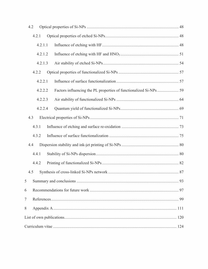
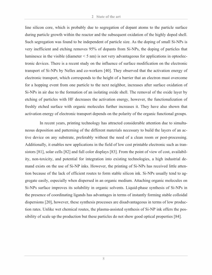
In a microwave plasma reactor, particle formation and growth take place in the gas-phase. In this
approach, gases (such as Ar and H2) are injected into the reaction chamber and microwave en-
ergy is used to generate the plasma. When precursor gas is delivered into the reaction chamber,
the decomposition of precursor molecules takes place mostly due to the high temperature of the
plasma and a supersaturated vapor of the growth species is formed [85]. If the degree of super-
saturation is sufficient, homogeneous nucleation occurs and particles nuclei are formed. Once
nuclei are generated, the particles are formed by coagulation and coalescence process. Apart
from these processes, undecomposed or partially decomposed precursors take part in the growth
of particles by surface reaction. A schematic representation of the different processes in a mi-
crowave plasma reactor is shown in Fig. 3.1.
Fig. 3.1. Schematic representation of different processes in a microwave plasma reactor.
3 Methodologies
10
For the synthesis of Si-NPs, silane (SiH4) is used as a precursor gas. The decomposition
of silane can be summarized by the following simplified equation [86],
2k
4 2HSi SiH � � (3.1)
The reaction rate can be described by a first-order rate law, which can be written as,
pp kN
dtdN
�� (3.2)
where Np is the number density of SiH4 molecules and k is the reaction rate constant,
���
����
���
TkEkk
b
aexp0 (3.3)
where k0 is the pre-exponential factor, Ea is activation energy, T is temperature and kb is the
Boltzmann constant. From shock-tube experiments, the values of k0 and Ea/ kb are determined to
be 2�108 and 14140 K, respectively [87, 88].
After the pyrolysis of precursor, clusters (nuclei) are formed from the supersaturated
vapor of primary growth species. Only the clusters with sizes greater than the critical cluster size
grow further. The radius of critical cluster (r*) is given by [89],
)ln(
2*
s
m
ppRT
Vr �� (3.4)
where � is the surface energy, Vm is the molar volume, R is the universal gas constant, p is the
partial pressure of primary growth species and ps is the equilibrium vapor pressure of clusters of
radius r.
The particles inside the reaction chamber collide and stick to each other to form bigger
particles. This process is known as coagulation. The characteristic time for coagulation (�c) is
defined as the time needed to reduce the number density of the particles to half of its initial value
and is given by [90],
Ncc �
� 1� (3.5)
where �c is the collision frequency function and N is the number density of particles.
3 Methodologies
11
The coagulation is followed by coalescence, which is a strong function of temperature,
particle size and material property. The characteristic time for coalescence (�s) that is needed to
reduce the excess surface area of agglomerate over that of a sphere of the same mass by a factor
of 0.63 is given by [91],
���
����
��
�
TkED
Td
b
D
NPs
exp0
4
�� (3.6)
where dNP is the primary particle diameter, ED is the activation energy for diffusion and D0 is the
diffusion coefficient.
Depending on the characteristic time for coagulation (�c) and coalescence (�s), either
soft agglomerates (�c � �s), hard agglomerates (�c < �s) or non-agglomerated spherical particles
(�c >> �s) are formed [92].
3.1.1.2 Experimental details
In this synthesis approach, an Ar-SiH4 gas mixture (1–10% SiH4 in Ar) was used as a precursor
gas. The operating pressure in the reaction chamber was maintained between 1 to 1000 mbar.
The microwave generator with frequency of 2.45 GHz and the maximum microwave power of
6000 W was used. After the synthesis, the particles were collected from the filter for further in-
vestigations. The results of Si-NPs, synthesized using different experimental conditions, are pre-
sented in Sect. 4.1.1.
3.1.2 Etching of Si-NPs
3.1.2.1 Background
If silicon is exposed to air, the surface undergoes oxidation and a thin oxide layer is formed on it.
One of the most widely used techniques to remove the oxide layer from the surface of silicon is
to etch it with aqueous HF. HF is a weak acid and it does not fully dissociate in the solution. Fur-
3 Methodologies
12
thermore, it can dimerize and the dimers can release one proton (H+). The equilibrium constants
between the H+, F–, HF2– and H2F2 species at 25°C are [93, 94],
41085.6[HF]
]][F[H ���
�� mol/m3 (3.7)
963.3] [HF][F
][HF2 ��
�
m3/mol (3.8)
2.7 [HF]]F[H2
22 � m3/mol (3.9)
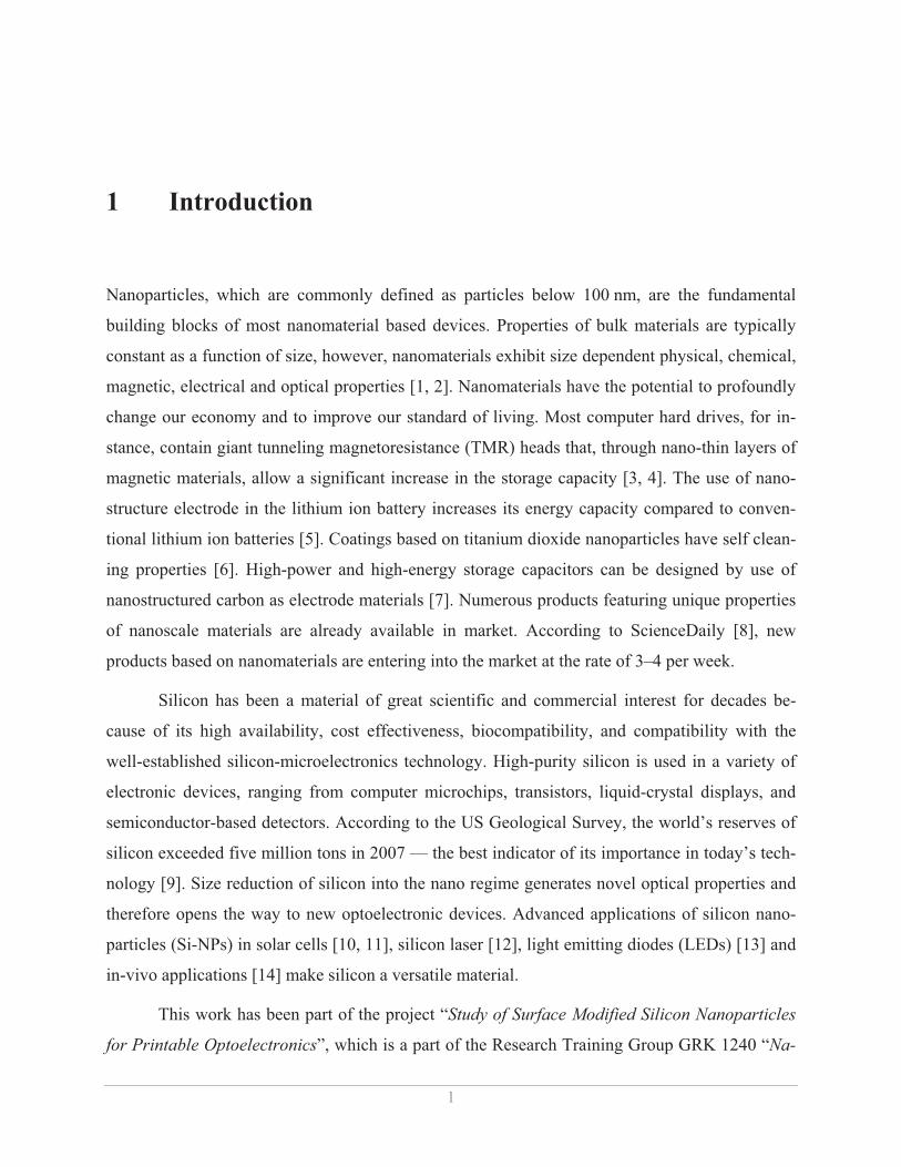
The etching of silicon surface with HF solution involves the dissolution of silicon oxide
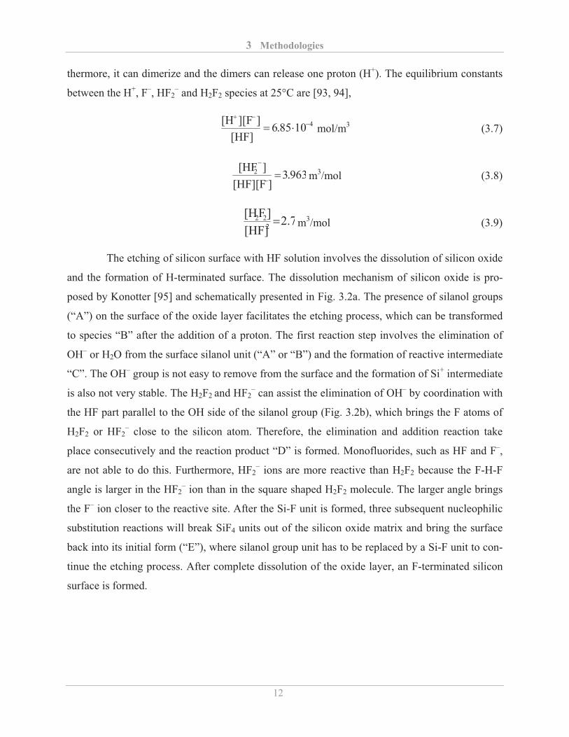
and the formation of H-terminated surface. The dissolution mechanism of silicon oxide is pro-
posed by Konotter [95] and schematically presented in Fig. 3.2a. The presence of silanol groups
(“A”) on the surface of the oxide layer facilitates the etching process, which can be transformed
to species “B” after the addition of a proton. The first reaction step involves the elimination of
OH– or H2O from the surface silanol unit (“A” or “B”) and the formation of reactive intermediate
“C”. The OH– group is not easy to remove from the surface and the formation of Si+ intermediate
is also not very stable. The H2F2 and HF2– can assist the elimination of OH– by coordination with
the HF part parallel to the OH side of the silanol group (Fig. 3.2b), which brings the F atoms of
H2F2 or HF2– close to the silicon atom. Therefore, the elimination and addition reaction take
place consecutively and the reaction product “D” is formed. Monofluorides, such as HF and F–,
are not able to do this. Furthermore, HF2– ions are more reactive than H2F2 because the F-H-F
angle is larger in the HF2– ion than in the square shaped H2F2 molecule. The larger angle brings
the F– ion closer to the reactive site. After the Si-F unit is formed, three subsequent nucleophilic
substitution reactions will break SiF4 units out of the silicon oxide matrix and bring the surface
back into its initial form (“E”), where silanol group unit has to be replaced by a Si-F unit to con-
tinue the etching process. After complete dissolution of the oxide layer, an F-terminated silicon
surface is formed.
3 Methodologies
13
Fig. 3.2. (a) Reaction mechanism of the dissolution of silicon oxide in aqueous HF. (b) HF2– as-
sisted OH– elimination reaction with consecutive F– addition.
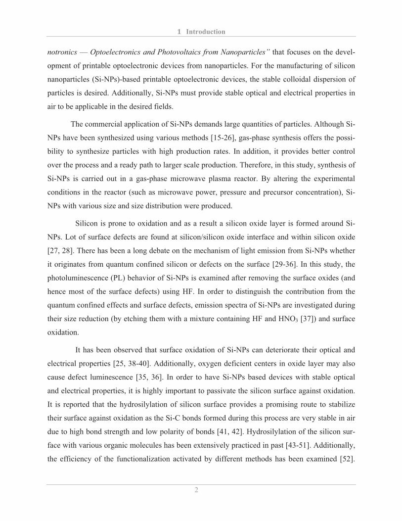
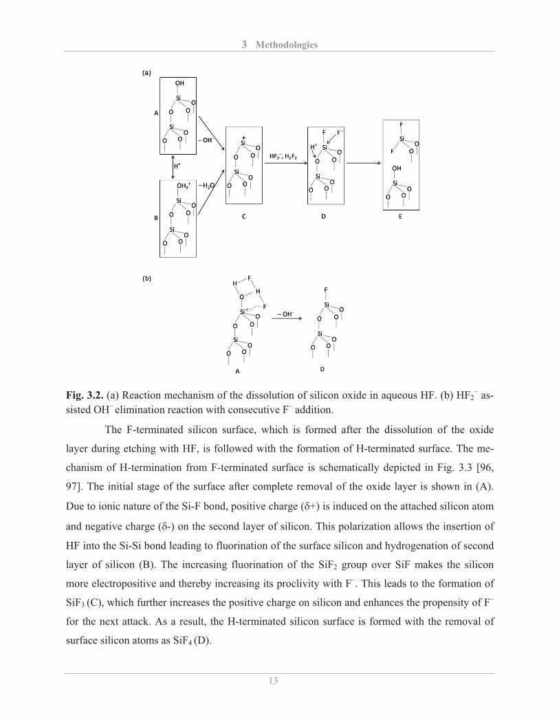
The F-terminated silicon surface, which is formed after the dissolution of the oxide
layer during etching with HF, is followed with the formation of H-terminated surface. The me-
chanism of H-termination from F-terminated surface is schematically depicted in Fig. 3.3 [96,
97]. The initial stage of the surface after complete removal of the oxide layer is shown in (A).
Due to ionic nature of the Si-F bond, positive charge (�+) is induced on the attached silicon atom
and negative charge (�-) on the second layer of silicon. This polarization allows the insertion of
HF into the Si-Si bond leading to fluorination of the surface silicon and hydrogenation of second
layer of silicon (B). The increasing fluorination of the SiF2 group over SiF makes the silicon
more electropositive and thereby increasing its proclivity with F–. This leads to the formation of
SiF3 (C), which further increases the positive charge on silicon and enhances the propensity of F–
for the next attack. As a result, the H-terminated silicon surface is formed with the removal of
surface silicon atoms as SiF4 (D).
3 Methodologies
14
Fig. 3.3. Schematic representation of the formation of H-terminated silicon surface.
3.1.2.2 Experimental details
In this work, the etching of Si-NPs was carried out with HF in a glove box under a dry nitrogen
atmosphere. In a typical experiment, 40 mg of as-synthesized Si-NPs were dispersed into 5 ml of
methanol using mild sonication and thereafter they were etched inside the glove box with 10 ml
of HF (49 wt. %). The dispersion was stirred for about 5 min at room temperature and then the
particles were filtered on a polyvinylidene fluoride (PVDF) membrane filter (pore size 0.1 �m).
For the size reduction of Si-NPs, a mixture containing HF (10 ml, 49 wt. %) and HNO3 (1 ml, 69
wt. %) was added to the suspension of Si-NPs in methanol. The solution was vigorously stirred
during the process to achieve homogeneous etching. The etching procedure was stopped by dilut-
ing the solution with methanol and immediate filtration of particles on a filter. After the filtra-
tion, particles were rinsed with HF and dispersed in a solvent. Thereafter, the suspension was
transported from the glove box to the measurement setup within an airtight glass bottle in order
to avoid air exposure. The experimental results of etched Si-NPs are presented in Sect. 4.1.2.
3.1.3 Surface functionalization of Si-NPs
3.1.3.1 Background
Attaching molecular layers on silicon surface has been the focus of much attention due to its
ability to control the chemical, electrical and optical properties of the underlying silicon. Chemi-
cal properties, such as polarity or hydrophilicity can be tuned by engineering the functional
3 Methodologies
15
group attached to silicon surface [43, 98-100]. Electrical properties such as conductance through
silicon-based circuits can be modulated with the absorption of unique organic molecules [101].
Additionally, it is seen that that the organic group on silicon surface alter its energy band and
therefore change its optical properties [53].
Attachment of organic molecules can be carried out on the oxidized as well as H-
terminated silicon surfaces [102-104]. The oxide layer on silicon surface is not desired for cer-
tain applications (e.g. solar cells) due to its insulating nature. Also, the formation of organic mo-
nolayer on the oxidized surface separates the underlying crystalline silicon from any functionali-
ty placed on the top. Hydrosilylation of H-terminated silicon surface with alkene or alkynes is
one of the most effective and delicate method to synthesize organosilicon compounds as it allows
the attachment of the chemical functionalities directly to the silicon through a Si–C bond.
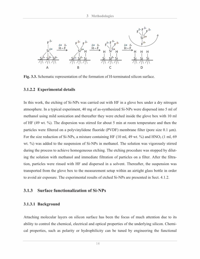
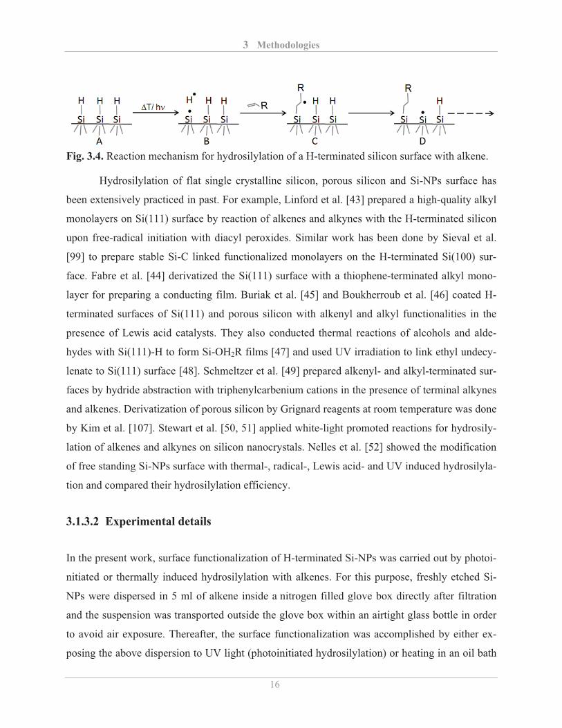
The mechanism of hydrosilylation of silicon surface with alkenes is schematically pre-
sented in Fig. 3.4 [104]. The H-terminated silicon surface that is obtained directly after HF etch-
ing is shown in (A). The reaction starts with a homolytic cleavage of the surface Si-H bonds,
which can be achieved by several methods such as free radical initiators, thermal energy (ther-
mally induced hydrosilylation) and UV light (photoinitiated hydrosilylation). Due to homolytic
cleavage of the surface Si-H bond, a silicon dangling bond is formed (B). The silicon dangling
bond is believed to react with the C=C bond of an alkene to form the Si-C bond and leaving a �-
CH radical on the immobilized organic molecule (C). Thereafter, the remaining carbon based
radical abstracts hydrogen from the neighboring Si-H group (D) and the new silicon dangling
bond allows the hydrosilylation reaction to proceed. This mechanism has been verified by a
number of experimental studies. For example, scanning tunneling microscopy (STM) has been
used to directly observe the growth of molecular island formation around isolated reaction initia-
tion sites [105, 106]. Additionally, studies using deuterated silicon (with surface Si-D bonds)
have shown that as the reaction proceeds, deuterium incorporation into the organic film (as C-D)
occurs [106]. The white light activated hydrosilylation reaction based on the absorption of a pho-
ton from the silicon crystal, formation of an exciton and interaction of the free exciton with an
alkene is also proposed [104].
3 Methodologies
16
Fig. 3.4. Reaction mechanism for hydrosilylation of a H-terminated silicon surface with alkene.
Hydrosilylation of flat single crystalline silicon, porous silicon and Si-NPs surface has
been extensively practiced in past. For example, Linford et al. [43] prepared a high-quality alkyl
monolayers on Si(111) surface by reaction of alkenes and alkynes with the H-terminated silicon
upon free-radical initiation with diacyl peroxides. Similar work has been done by Sieval et al.
[99] to prepare stable Si-C linked functionalized monolayers on the H-terminated Si(100) sur-
face. Fabre et al. [44] derivatized the Si(111) surface with a thiophene-terminated alkyl mono-
layer for preparing a conducting film. Buriak et al. [45] and Boukherroub et al. [46] coated H-
terminated surfaces of Si(111) and porous silicon with alkenyl and alkyl functionalities in the
presence of Lewis acid catalysts. They also conducted thermal reactions of alcohols and alde-
hydes with Si(111)-H to form Si-OH2R films [47] and used UV irradiation to link ethyl undecy-
lenate to Si(111) surface [48]. Schmeltzer et al. [49] prepared alkenyl- and alkyl-terminated sur-
faces by hydride abstraction with triphenylcarbenium cations in the presence of terminal alkynes
and alkenes. Derivatization of porous silicon by Grignard reagents at room temperature was done
by Kim et al. [107]. Stewart et al. [50, 51] applied white-light promoted reactions for hydrosily-
lation of alkenes and alkynes on silicon nanocrystals. Nelles et al. [52] showed the modification
of free standing Si-NPs surface with thermal-, radical-, Lewis acid- and UV induced hydrosilyla-
tion and compared their hydrosilylation efficiency.
3.1.3.2 Experimental details
In the present work, surface functionalization of H-terminated Si-NPs was carried out by photoi-
nitiated or thermally induced hydrosilylation with alkenes. For this purpose, freshly etched Si-
NPs were dispersed in 5 ml of alkene inside a nitrogen filled glove box directly after filtration
and the suspension was transported outside the glove box within an airtight glass bottle in order
to avoid air exposure. Thereafter, the surface functionalization was accomplished by either ex-
posing the above dispersion to UV light (photoinitiated hydrosilylation) or heating in an oil bath
3 Methodologies
17
(thermally induced hydrosilylation). The wavelength of UV light and the temperature used for
functionalization is mentioned in each section of the results and discussion part separately. In
photoinitiated hydrosilylation, the alkene and Si-NPs dispersion was exposed from all directions
with UV light. A triangular shaped UV reactor, containing two NU81-254 nm/366 nm VWR UV
light source at each triangular position, was used for this purpose. However, the surface functio-
nalization of particles discussed in Sect. 4.2.2.1 was carried out using a Rayonet photochemical
cylindrical reactor equipped with 16RPR-254 nm UV tubes. The dispersion was stirred conti-
nuously during the UV exposure/heating in oil bath for homogeneous reaction.
3.1.4 Ink-jet printing of Si-NPs
3.1.4.1 Background
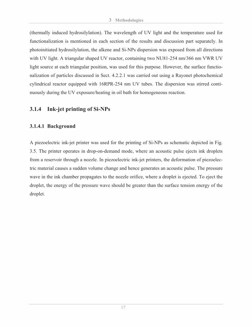
A piezoelectric ink-jet printer was used for the printing of Si-NPs as schematic depicted in Fig.
3.5. The printer operates in drop-on-demand mode, where an acoustic pulse ejects ink droplets
from a reservoir through a nozzle. In piezoelectric ink-jet printers, the deformation of piezoelec-
tric material causes a sudden volume change and hence generates an acoustic pulse. The pressure
wave in the ink chamber propagates to the nozzle orifice, where a droplet is ejected. To eject the
droplet, the energy of the pressure wave should be greater than the surface tension energy of the
droplet.
3 Methodologies
18
Fig. 3.5. Schematic diagram of piezoelectric ink-jet printer [108].
3.1.4.2 Experimental details
In the present study, a colloidal dispersion of functionalized Si-NPs in ethyl undecylenate was
used to fabricate films on glass substrates using a piezoelectric Dimatix 2800 ink-jet printer. This
printer can create and define patterns over an area of about 200 × 300 mm2 and handle substrates
up to 25 mm thick with an adjustable vertical height. Prior to printing, the glass substrates were
cleaned in piranha solution (3:1 volumetric mixture of sulfuric acid and hydrogen peroxide) for
30 min followed by rinsing several times in water and dried in a stream of nitrogen. A very low
concentration of particles in the ink (~ 0.4 wt. %) was prepared with a viscosity of 2.3 mPa/s and
a surface tension of 31 mN/m. The cartridge was filled with 1.5 ml of Si-NPs dispersion and the
droplet volume jetted from the cartridge was equal to 10 picoliter. The printing was carried out at
13 V and a frequency of 3 kHz. The substrate temperature was set at 60°C and multiple layers of
Si-NPs were printed on the substrate in a layer-by-layer fashion. The computer controlled print
head was moved in two dimensions to write structures on the substrate. There was a 10 min de-
lay between two successively printed layers.
3 Methodologies
19
3.2 Characterization
3.2.1 X-ray diffraction (XRD)
3.2.1.1 Background
X-ray diffraction (XRD) is a characterization technique by which the arrangement of atoms with-
in a crystal can be determined. Additionally, it can also provide other information about the ma-
terial such as average crystallite size and residual stress. XRD is based on the phenomenon of the
wave interferences, in which two electromagnetic waves with the same wavelength travelling in
the same direction can either reinforce or cancel each other depending on their phase difference.
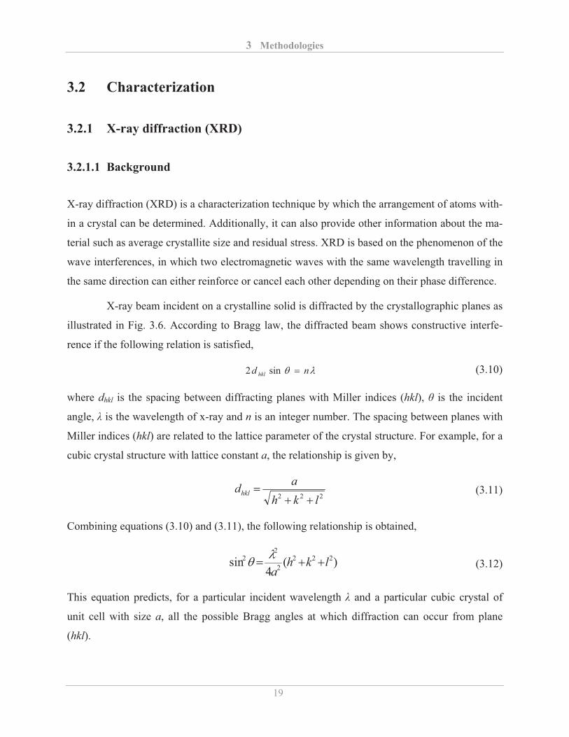
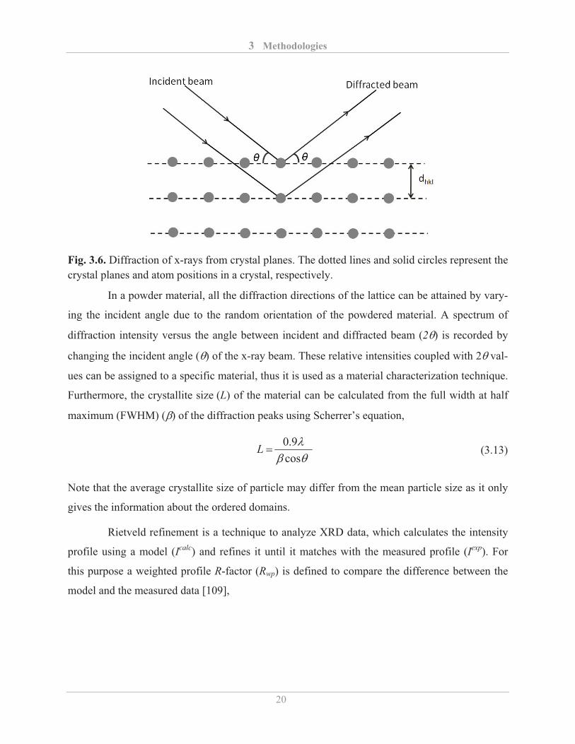
X-ray beam incident on a crystalline solid is diffracted by the crystallographic planes as
illustrated in Fig. 3.6. According to Bragg law, the diffracted beam shows constructive interfe-
rence if the following relation is satisfied,
� nd hkl �sin2 (3.10)
where dhkl is the spacing between diffracting planes with Miller indices (hkl), � is the incident
angle, � is the wavelength of x-ray and n is an integer number. The spacing between planes with
Miller indices (hkl) are related to the lattice parameter of the crystal structure. For example, for a
cubic crystal structure with lattice constant a, the relationship is given by,
222 lkhadhkl
��� (3.11)
Combining equations (3.10) and (3.11), the following relationship is obtained,
)(4
sin 2222
22 lkh
a���
� (3.12)
This equation predicts, for a particular incident wavelength � and a particular cubic crystal of
unit cell with size a, all the possible Bragg angles at which diffraction can occur from plane
(hkl).
3 Methodologies
20
Fig. 3.6. Diffraction of x-rays from crystal planes. The dotted lines and solid circles represent the crystal planes and atom positions in a crystal, respectively.
In a powder material, all the diffraction directions of the lattice can be attained by vary-
ing the incident angle due to the random orientation of the powdered material. A spectrum of
diffraction intensity versus the angle between incident and diffracted beam (2) is recorded by
changing the incident angle () of the x-ray beam. These relative intensities coupled with 2 val-
ues can be assigned to a specific material, thus it is used as a material characterization technique.
Furthermore, the crystallite size (L) of the material can be calculated from the full width at half
maximum (FWHM) (�) of the diffraction peaks using Scherrer’s equation,
��
cos9.0
�L (3.13)
Note that the average crystallite size of particle may differ from the mean particle size as it only
gives the information about the ordered domains.
Rietveld refinement is a technique to analyze XRD data, which calculates the intensity
profile using a model (Icalc) and refines it until it matches with the measured profile (Iexp). For
this purpose a weighted profile R-factor (Rwp) is defined to compare the difference between the
model and the measured data [109],
3 Methodologies
21
� �� �
� ��
�
�
�
�� N
iii
N
i
calciii
wp
Iw
IIwR
1
2exp
1
2exp
(3.14)
where wi is equal to (Iiexp)–0.5. The value of Rwp indicates the quality of the fit. The lower the val-
ue of Rwp, the better the agreement between the model and the measured data.
3.2.1.2 Experimental details
In this study, the crystalline structure and crystallite size of Si-NPs were determined by XRD
using a PANalytical x-ray diffractometer (X´Pert PRO). The diffractometer is equipped with Ni-
filtered Cu-K� (1.54 Å) x-ray radiation source operated at 40 kV and 40 mA. The diffraction data
(2� = 20° to 120°) were analyzed by Rietveld refinement with the help of the MAUD program
[109].
3.2.2 Transmission electron microscopy (TEM)
3.2.2.1 Background
Transmission electron microscopy (TEM) is a powerful technique to investigate the crystallo-
graphic structure, defects, interfaces and grain boundaries as it provides resolution down to the
atomic level. The transmission electron microscope functions similar to a light microscope. The
main difference is that the electrons are focused on a substrate with the aid of the electromagnet-
ic lens in the TEM instead of glass lenses for visible light in a light microscope. In TEM, the
electrons are generated either by thermionic emission (e.g. electrically heated LaB6 filament) or
by field emission (e.g. tungsten filament). In thermionic emission, the electrons are generated by
heating the cathode filament to a high temperature. If the thermal energy is sufficiently high that
electrons can overcome the work function, then the electrons can leave the material. In field
emission, electrons tunnel out of the material when an intense field is applied to it, therefore, it
requires a very sharp, needle-shaped cathode.
3 Methodologies
22
In TEM, image contrast arises because of the scattering of the incident beam by the
sample. The electron wave can change both the amplitude and phase as it transverses the sample,
and both kinds of change give rise to image contrast. In TEM different types of contrasts can be
arise, such as diffraction contrast, mass-thickness contrast and phase contrast. Coherent elastic
interaction of electrons with crystalline object produces diffraction contrast in the TEM image.
The mass-thickness contrast arises from incoherent (Rutherford) elastic scattering of electrons. A
phase contrast image requires the selection of more than one beam (two or more beams). The
contrast in image is formed by either constructive or destructive interference of beams.
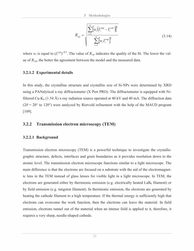
TEM can be used in different imaging modes. These modes can be chosen by selecting
either the undiffracted beam or the diffracted beam or both (Fig. 3.7). If the objective aperture is
selected such that it only allows the direct beam to pass, a bright field (BF) image is formed. If
the diffracted beam is only allowed to pass through the objective aperture, a dark field (DF) im-
age is formed. Mass thickness and diffraction contrast contribute to the image in these modes.
Areas belonging to crystalline regions selecting their Bragg beams appear with bright contrast in
DF mode and dark in BF imaging mode. A high resolution TEM (HR-TEM) image is formed by
allowing the directed beam together with diffracted beams through the aperture. In HR-TEM,
only phase contrast contributes to the image.
Fig. 3.7. Schematic illustration of the formation of bright field image (left), dark field image (middle) and HR-TEM image (right). Reproduced from [110].
3 Methodologies
23
3.2.2.2 Experimental details
In the present work, the crystallinity, size, shape and morphology of Si-NPs were analyzed by
using conventional TEM (Philips CM-12, operating at 120 kV) and HR-TEM (Philips CM-20,
operating at 200 kV). Samples for TEM were prepared by immersing the carbon-coated copper
grids into a dispersion of the Si-NPs in methanol/chloroform, followed by evaporation of the
solvent.
3.2.3 Impedance spectroscopy (IS)
3.2.3.1 Background
Impedance spectroscopy (IS) is a technique to study electrical properties of a material. In this
process, an electrical AC stimulus (a known AC voltage or current) is applied to a material (de-
posited between two electrodes) and the corresponding response (voltage or current) is analyzed
[111]. It is assumed that the properties of electrode-material system are time invariant. Several
methods exist to induce stimuli for impedance measurement. However, the most common ap-
proach involves the measurement of impedance directly in the frequency domain by applying a
single-frequency AC voltage to the interface. The measurements can be performed over a wide
frequency range from mHz to MHz. Each measurement is consequently followed by measuring
the phase shift as well as the amplitude of the resulting signal at that frequency.
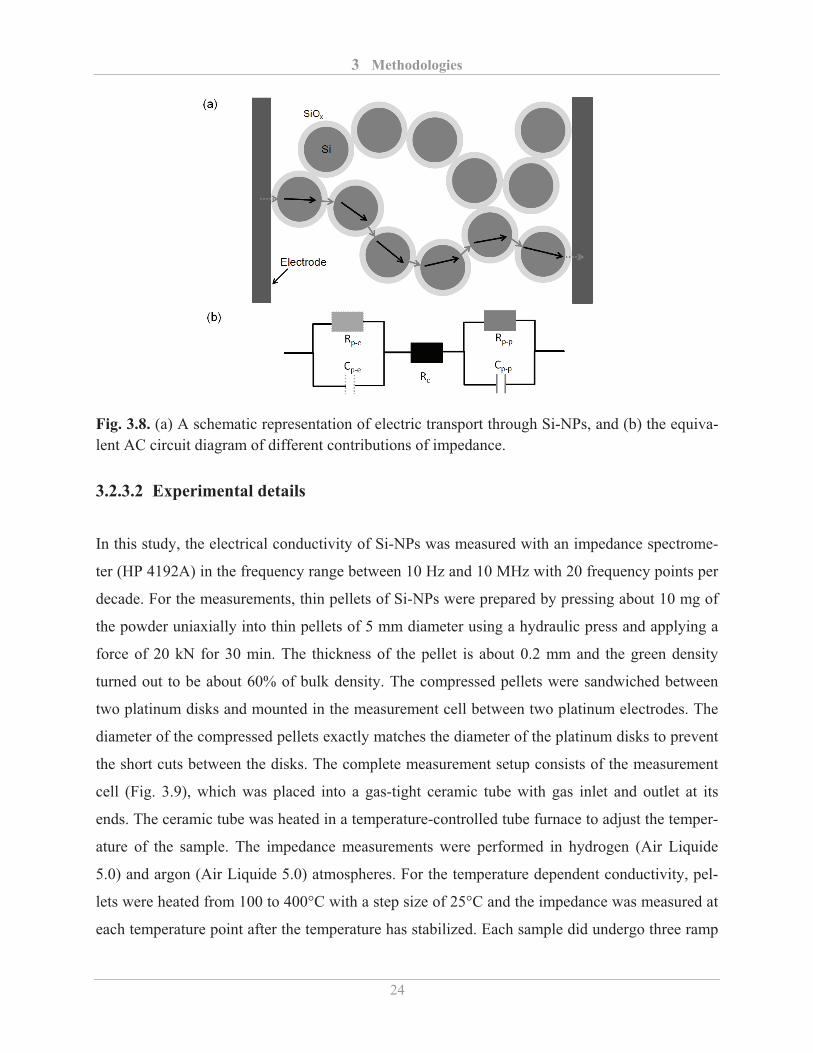
The electric transport through a percolation network of Si-NPs (e.g. a compressed
powder) can be represented by a simplified sketch as shown in Fig. 3.8a. The total impedance
measured from Si-NPs pellets should come from three different contributions; particle-electrode
contact, particle core and particle-particle contacts. Figure 3.8b shows the equivalent circuit dia-
gram of different contributions of impedance. The resistors Rc account for the contribution of the
core of Si-NPs, whereas, the particle-particle contacts can be represented by a resistor Rp-p and a
capacitor Cp-p in parallel. Similarly, the particle-electrode contact can be represented by a resistor
Rp-e and a capacitor Cp-e in parallel. A typical representation of the total impedance (Z) is com-
posed of a real part (Z´) and an imaginary part (Z´´). If the real part is plotted on the horizontal
axis and the imaginary part on the vertical axis, this representation is called “Nyquist plot”.
3 Methodologies
24
Fig. 3.8. (a) A schematic representation of electric transport through Si-NPs, and (b) the equiva-lent AC circuit diagram of different contributions of impedance.
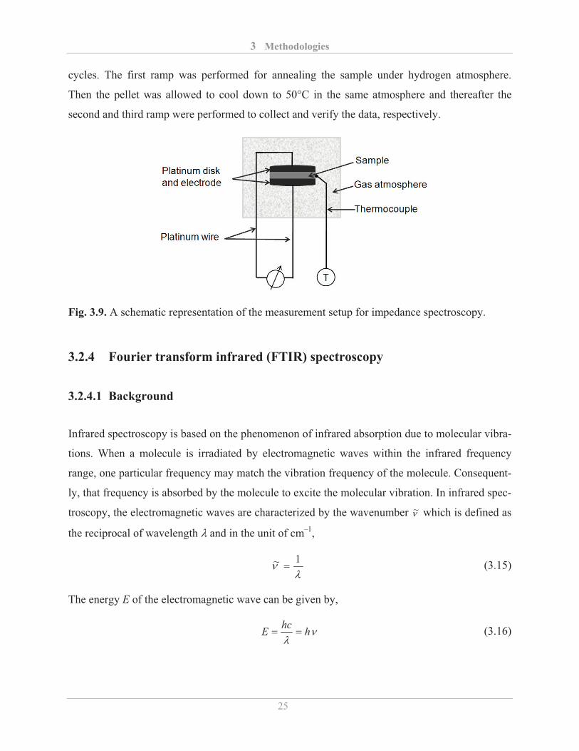
3.2.3.2 Experimental details
In this study, the electrical conductivity of Si-NPs was measured with an impedance spectrome-
ter (HP 4192A) in the frequency range between 10 Hz and 10 MHz with 20 frequency points per
decade. For the measurements, thin pellets of Si-NPs were prepared by pressing about 10 mg of
the powder uniaxially into thin pellets of 5 mm diameter using a hydraulic press and applying a
force of 20 kN for 30 min. The thickness of the pellet is about 0.2 mm and the green density
turned out to be about 60% of bulk density. The compressed pellets were sandwiched between
two platinum disks and mounted in the measurement cell between two platinum electrodes. The
diameter of the compressed pellets exactly matches the diameter of the platinum disks to prevent
the short cuts between the disks. The complete measurement setup consists of the measurement
cell (Fig. 3.9), which was placed into a gas-tight ceramic tube with gas inlet and outlet at its
ends. The ceramic tube was heated in a temperature-controlled tube furnace to adjust the temper-
ature of the sample. The impedance measurements were performed in hydrogen (Air Liquide
5.0) and argon (Air Liquide 5.0) atmospheres. For the temperature dependent conductivity, pel-
lets were heated from 100 to 400°C with a step size of 25°C and the impedance was measured at
each temperature point after the temperature has stabilized. Each sample did undergo three ramp
3 Methodologies
25
cycles. The first ramp was performed for annealing the sample under hydrogen atmosphere.
Then the pellet was allowed to cool down to 50°C in the same atmosphere and thereafter the
second and third ramp were performed to collect and verify the data, respectively.
Fig. 3.9. A schematic representation of the measurement setup for impedance spectroscopy.
3.2.4 Fourier transform infrared (FTIR) spectroscopy
3.2.4.1 Background
Infrared spectroscopy is based on the phenomenon of infrared absorption due to molecular vibra-
tions. When a molecule is irradiated by electromagnetic waves within the infrared frequency
range, one particular frequency may match the vibration frequency of the molecule. Consequent-
ly, that frequency is absorbed by the molecule to excite the molecular vibration. In infrared spec-
troscopy, the electromagnetic waves are characterized by the wavenumber ~ which is defined as
the reciprocal of wavelength � and in the unit of cm–1,
�
1~ � (3.15)
The energy E of the electromagnetic wave can be given by,
�
hhcE �� (3.16)
3 Methodologies
26
where is the frequency of electromagnetic wave, h is the Planck´s constant and c is the speed of
light. Therefore, the wavenumber can also be expressed as,
hcE
c��
~ (3.17)
It is clear from the above expression that the wavenumber is directly proportional to the energy
of the electromagnetic wave. The infrared spectrum ranges from 4000 to 400 cm–1.
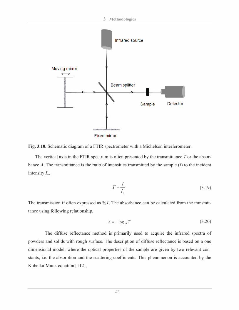
Fourier transform infrared spectroscopy (FTIR) is an infrared spectroscopy technique in
which the Fourier transformation method is used to obtain an infrared spectrum in the whole
range of wavenumber simultaneously. It differs from the dispersive method, which entails creat-
ing a spectrum by collecting signals at each wavenumber separately. The principle of FTIR is
based on the Michelson interferometer, as schematically illustrated in Fig. 3.10. The infrared
beam splits into two beams by a beam splitter. The two beams strike a fixed mirror and a moving
mirror, respectively. The recombination of the two beams caused interference before passing the
sample. The function of the moving mirror is to change the path length between two split beams.
The two beams show constructive and destructive interference periodically with continuous
change in the path length. The plot of sum of all interference intensity, created by each wave-
length in the beam, as a function of optical path difference is called interferogram. The Fourier
transformation is performed by a computer to convert the interferogram into an infrared spec-
trum. The Fourier transformation between a function in time (t) domain and its corresponding
one in the frequency (�) domain is given by,
�
��
�� dtetfF ti�
!� )(
21)( (3.18)
The Fourier transformation converts the intensity versus the optical path difference to the intensi-
ty versus the wavenumber. The optical path difference can be considered to be in the time do-
main because it is obtained by multiplying time with the speed of a moving mirror. The wave-
number can be considered in the frequency domain as it is equal to the frequency divided by the
speed of light.
3 Methodologies
27
Fig. 3.10. Schematic diagram of a FTIR spectrometer with a Michelson interferometer.
The vertical axis in the FTIR spectrum is often presented by the transmittance T or the absor-
bance A. The transmittance is the ratio of intensities transmitted by the sample (I) to the incident
intensity Io,
oIIT � (3.19)
The transmission if often expressed as %T. The absorbance can be calculated from the transmit-
tance using following relationship,
TA 10log�� (3.20)
The diffuse reflectance method is primarily used to acquire the infrared spectra of
powders and solids with rough surface. The description of diffuse reflectance is based on a one
dimensional model, where the optical properties of the sample are given by two relevant con-
stants, i.e. the absorption and the scattering coefficients. This phenomenon is accounted by the
Kubelka-Munk equation [112],
3 Methodologies
28
SK
RRRf �
��
�
�� 2
)1()(2
(3.21)
where K denotes the absorption modulus, S is the scattering modulus and R� is the degree of ref-
lection on the sample with sufficient thickness that no radiation reaches the back surface.
3.2.4.2 Experimental details
In the present work, FTIR measurements on Si-NPs were carried out at room temperature using a
Bruker IFS66v/S spectrometer. The spectra were measured in the wavenumber range from 800
cm–1 to 3100 cm–1. An average of 100 scans was acquired at a spectral resolution of 2 cm–1. The
measurements in transmission mode were performed by making thin pellets of potassium bro-
mide (KBr) and Si-NPs mixture. The mixture was prepared by spreading a few drops of chloro-
form dispersion of Si-NPs onto a mortar and blending with KBr powder after the evaporation of
chloroform. The diffused reflectance measurements were performed directly on dry powders.
FTIR spectra of functionalized Si-NPs were taken after separating the particles from their respec-
tive alkene solution by centrifugation, subsequent washing with methanol and drying in vacuum.
3.2.5 Electron paramagnetic resonance (EPR) spectroscopy
3.2.5.1 Background
Electron paramagnetic resonance (EPR) spectroscopy is based on the interaction between elec-
tromagnetic radiation and magnetic moment of electrons. In this method, the resonance absorp-
tion of microwave radiation by paramagnetic molecules or ion centers, containing at least one
unpaired electron, is studied in the presence of a magnetic field.
The basic physical concepts of EPR are analogous to those of nuclear magnetic reson-
ance (NMR), but it is electron spins that are excited instead of spins of atomic nuclei. Every elec-
tron has a magnetic moment and spin quantum number s = 1/2, with magnetic components ms =
+1/2 and ms = –1/2. In the presence of an external magnetic field, the magnetic moment of elec-
tron aligns itself either antiparallel (ms = +1/2) or parallel (ms = –1/2) to the field. This effect is
called Zeeman effect. The antiparallel and parallel alignments correspond to the higher energy
3 Methodologies
29
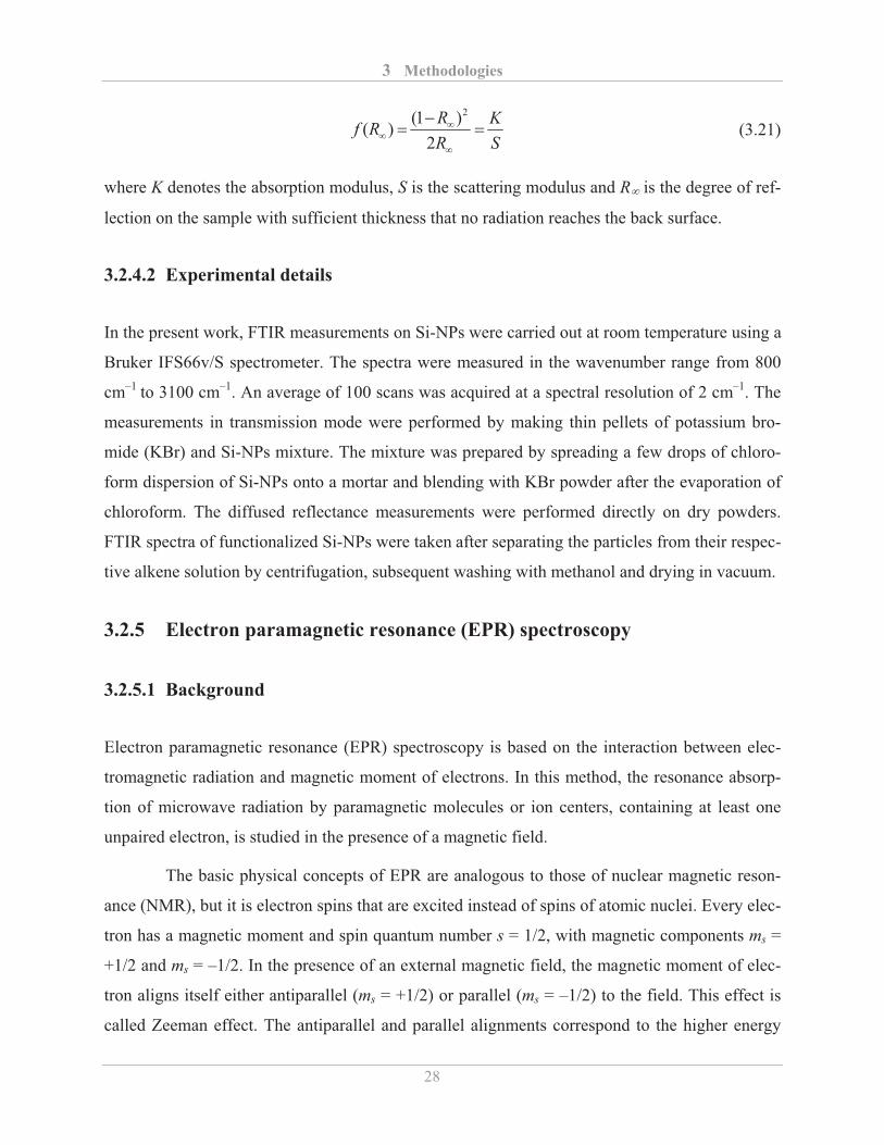
(E�) and lower energy (E�) state, respectively (Fig. 3.11). The energy separation �E�-� between
parallel and antiparallel alignments depends on the magnetic field B according to the following
equation,
BgEEE B����� ���� � (3.22)
where �B is the Bohr magneton and g is called g-factor (spectroscopic splitting factor). For an
electron in vacuum, g is equal to 2.00232 [113].
Fig. 3.11. Energy-level diagram for a single electron in vacuum as a function of external magnet-ic field.
In thermal equilibrium, the � and � states are distributed in such a way that more elec-
trons are in the lower state. The ratio between number of � spins (N�) and number of � spins
(N�) depends on temperature and is given by the Boltzmann distribution law,
���
����
�����
�
����
� ��� �
TkBg
TkE
NN
b
B
b
���
�
� expexp (3.23)
where kb is the Boltzmann constant and T is the absolute temperature. When the sample is placed
in a magnetic field and microwave radiation with frequency is applied, then the electron spin in
the � state absorbs this energy if the energy of the microwave radiation (h) coincides with the
energy difference between � and �,
Bgh B� � (3.24)
3 Methodologies
30
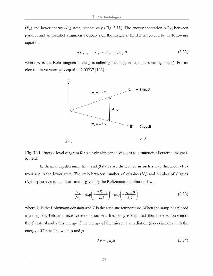
where h is Planck’s constant and is the frequency of the microwave radiation. The equation
(3.24) suggests that two possible ways for performing EPR experiment as illustrated in Fig. 3.12.
The first method consists of placing a spin ensemble in a constant magnetic field Bo and irradiat-
ing the sample with a linearly variable frequency (Fig. 3.12a). When the frequency matches the
resonance conditions for the magnetic field Bo, microwave radiation is absorbed and the absorp-
tion is revealed by a microwave detector. In an alternative way, the sample is irradiated with a
constant microwave frequency (o) in a linearly variable magnetic field (Fig. 3.12b). When the
magnetic field reaches the resonance condition, the microwave radiation is absorbed. In practice,
the measurements are performed by keeping the microwave frequency constant and recording its
absorption by varying the magnetic field.
Fig. 3.12. Two alternative ways to measure the EPR spectrum: (a) placing the sample in a con-stant magnetic field and varying the microwave frequency, and (b) irradiating the sample with a constant microwave frequency in a linearly variable magnetic field.
3.2.5.2 Experimental details
In the present study, the EPR measurements on Si-NPs were performed at room temperature with
a conventional continuous wave X-band spectrometer and a TE102 cavity (Bruker). For EPR
measurements, about 1 mg of particles were filled into small teflon tubes which were then placed
in a conventional Suprasil quartz EPR sample holder. A lock-in amplifier was used for the detec-
tion of the EPR signal with a modulation of the magnetic field at 100 kHz. All spectra were nor-
malized to the mass of the sample.
3 Methodologies
31
3.2.6 Photoluminescence (PL) spectroscopy
3.2.6.1 Background
Photoluminescence (PL) is the emission of radiation induced by the optical excitation of a sub-
stance with an external source of light. The PL emission from nanosized silicon has been exten-
sively studied in past [114-118]. Meier et al. [114], developed a model to compute the PL emis-
sion spectra of Si-NPs from a given size distribution. They observed that the oscillator strength,
which is proportional to the recombination rate of excitons, increases with increasing PL emis-
sion energy due to strong confinement in smaller nanoparticles. The energy dependence of the
oscillator strength (fosc) for Si-NPs is given by,
���
����
����� ��
0.332exp1080.5104.1 86 g
osc
Ef (3.25)
where Eg is electronic band gap of Si-NP in eV. According to Deleure et al. [119], the particle
size-dependent band gap of Si-NPs can be written as,
39.1073.3
NPg d
EE �� (3.26)
where E0 is the electronic band gap of bulk silicon in eV and dNP is the diameter of Si-NP in nm.
By introducing the effect of size dependent change in the lattice parameter of Si-NPs on the band
gap, Ledoux et al. [120] proposed a modified size dependent band gap for Si-NPs,
245.0881.073.339.10 ����
NPNPg dd
EE (3.27)
Meier et al. used equation (3.26) to calculate the size dependence of the oscillator strength,
���
����
����� ��
39.166 24.11exp107.1104.1
NPosc d
f (3.28)
For the particle size distribution, they assumed a lognormal size distribution,
���
����
���
g
pNP
gNPNP
gpNP ddddd
dddn��!
�2
2
ln2/ln
expln1
21),,( (3.29)
3 Methodologies
32
where dp is the mean particle diameter and �g is the geometrical standard deviation. Assuming
that each nanoparticle at room temperature acts as an inhomogeneous broadened emitter with a
spectral width of �E, which is in the order of few meV,the PL intensity of a single particle (INP)
with a peak emission energy of Eg can be given by,
� �� � �
�
�
�
��
�
�
�
��
�"� 2
2
2exp
21),,(
E
Eh
EEEhI g
gNP
! (3.30)
The PL emission of a nanoparticles ensemble with mean particle diameter dP and geometrical
standard deviation �g is given by,
NPNPEgNPNP
gpNPNPosc dddEhI
dddddn
dfhI ))(,(),,(
)()( ,0
�
�
� �
(3.31)
It has been shown that measured PL spectra of Si-NPs and those calculated using above model fit
nicely with each other [114].
3.2.6.2 Experimental details
In this study, different PL measurements on Si-NPs were performed at room temperature using
either a Nd:YAG laser as an excitation source operated at a wavelength of 532 nm, or a diode
laser operated at wavelength of 405 nm or a Perkin-Elmer LS 50 fluorescence spectrometer with
350 nm excitation. All the PL measurements were done at room temperature. All photographs of
luminescing Si-NPs were taken by exposing them with the UV lamp (� = 366 nm).
3.2.7 Photoluminescence quantum yield (QY)
3.2.7.1 Background
The photoluminescence quantum yield (QY) gives the efficiency of the photoluminescence
process. It is defined as the ratio of the number of photons emitted to the number of photons ab-
sorbed.
QY = number of photons emitted/ number of photons absorbed (3.32)
3 Methodologies
33
3.2.7.2 Experimental details
In order to measure the quantum yield of colloidal Si-NPs, a blue LED (� = 390 nm) was used to
excite the sample. First, the baseline PL measurement was performed using pure solvent in
which the particles were dispersed. The baseline measurement only shows the excitation peak of
the blue LED at 390 nm. In the second step, the PL of colloidal Si-NPs was measured, which has
a reduced intensity of the excitation peak at 390 nm due to absorption by Si-NPs and a PL emis-
sion peak. For the calculation of QY, the integration of the excitation and luminescence spectra
was performed. The following quantities were obtained,
�excitation
, )( ��� dIL bs (3.33)
and,
�luminesce
, )( ��� dIP sb (3.34)
where I(�) is the spectral irradiation and � is the wavelength. The subscript s and b denote the
sample and the baseline, respectively. If there is no luminescence signal in the baseline mea-
surement (Pb = 0), then the quantum yield can be calculated using following equation [121],
)(QY
bs
s
LLP��
� (3.35)
4 Results and discussion
34
4 Results and discussion
4.1 Synthesis and surface modification of Si-NPs
In this section, the synthesis of Si-NPs using a microwave plasma reactor is presented. Addition-
ally, the influence of etching and surface functionalization on the structural and surface proper-
ties of Si-NPs is examined.
4.1.1 Synthesis of Si-NPs
The microwave plasma reactor used for the synthesis of Si-NPs is schematically depicted in Fig.
4.1. The synthesis setup mainly consists of a quartz tube, microwave source and the gas delivery
system. Along with the diluent gases (Ar and H2), the precursor gas (SiH4 in Ar) is injected coax-
ially into the reaction chamber. The quartz tube is mounted within the microwave cavity, where
the microwave energy is coupled with gases and forms plasma. The decomposition of the precur-
sor takes place within the plasma, which eventually forms Si-NPs by nucleation and growth
processes (see Sect. 3.1.1 for details).
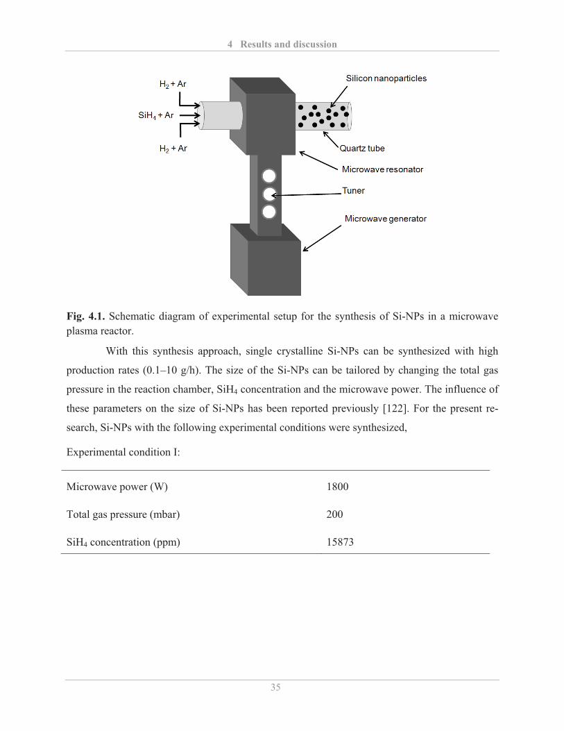
4 Results and discussion
35
Fig. 4.1. Schematic diagram of experimental setup for the synthesis of Si-NPs in a microwave plasma reactor.
With this synthesis approach, single crystalline Si-NPs can be synthesized with high
production rates (0.1–10 g/h). The size of the Si-NPs can be tailored by changing the total gas
pressure in the reaction chamber, SiH4 concentration and the microwave power. The influence of
these parameters on the size of Si-NPs has been reported previously [122]. For the present re-
search, Si-NPs with the following experimental conditions were synthesized,
Experimental condition I:
Microwave power (W) 1800
Total gas pressure (mbar) 200
SiH4 concentration (ppm) 15873
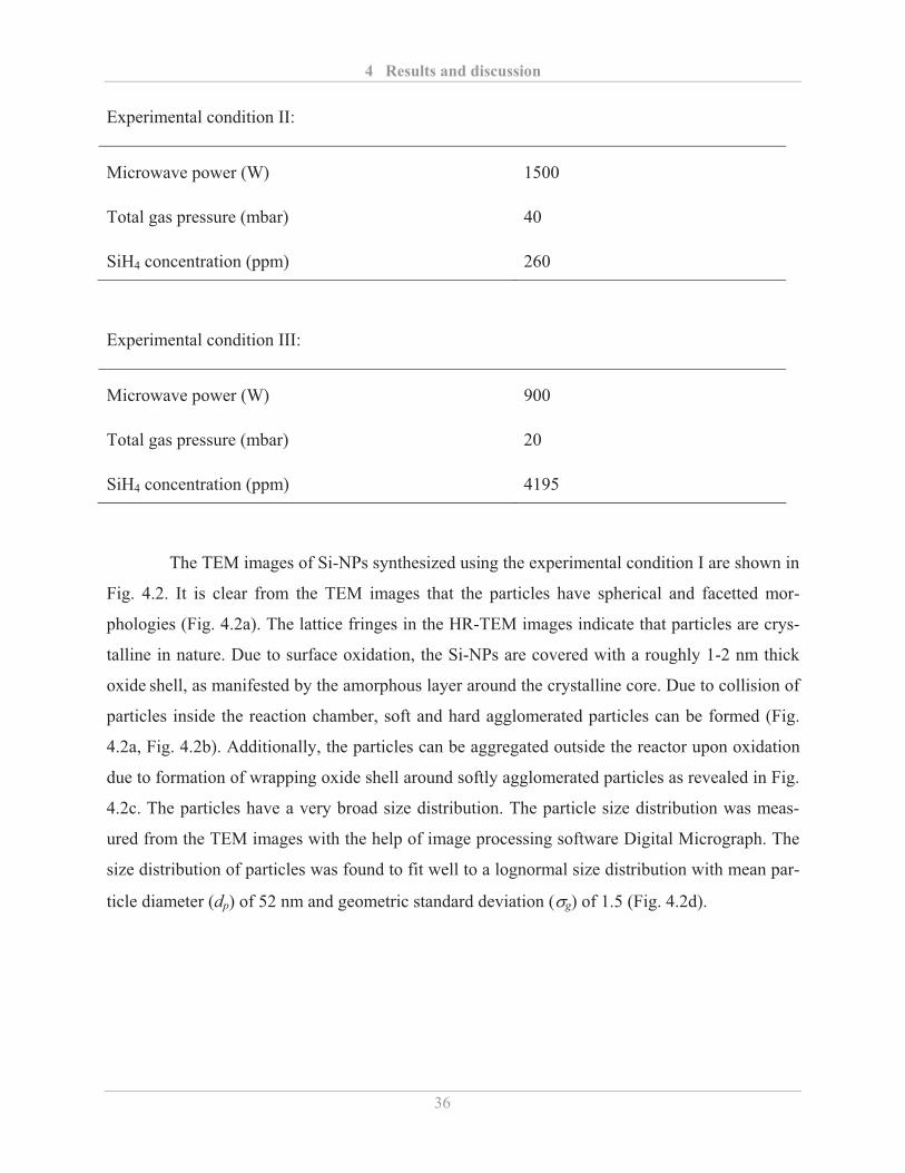
4 Results and discussion
36
Experimental condition II:
Microwave power (W) 1500
Total gas pressure (mbar) 40
SiH4 concentration (ppm) 260
Experimental condition III:
Microwave power (W) 900
Total gas pressure (mbar) 20
SiH4 concentration (ppm) 4195
The TEM images of Si-NPs synthesized using the experimental condition I are shown in
Fig. 4.2. It is clear from the TEM images that the particles have spherical and facetted mor-
phologies (Fig. 4.2a). The lattice fringes in the HR-TEM images indicate that particles are crys-
talline in nature. Due to surface oxidation, the Si-NPs are covered with a roughly 1-2 nm thick
oxide shell, as manifested by the amorphous layer around the crystalline core. Due to collision of
particles inside the reaction chamber, soft and hard agglomerated particles can be formed (Fig.
4.2a, Fig. 4.2b). Additionally, the particles can be aggregated outside the reactor upon oxidation
due to formation of wrapping oxide shell around softly agglomerated particles as revealed in Fig.
4.2c. The particles have a very broad size distribution. The particle size distribution was meas-
ured from the TEM images with the help of image processing software Digital Micrograph. The
size distribution of particles was found to fit well to a lognormal size distribution with mean par-
ticle diameter (dp) of 52 nm and geometric standard deviation (�g) of 1.5 (Fig. 4.2d).
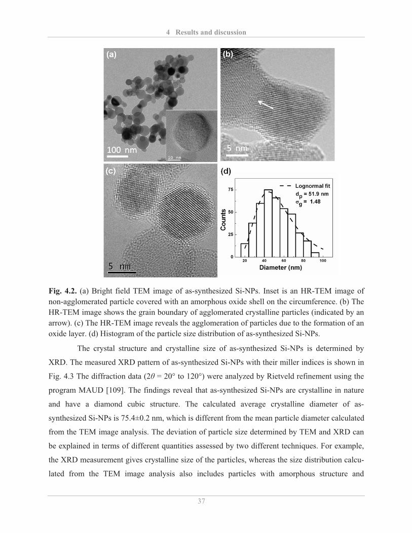
4 Results and discussion
37
Fig. 4.2. (a) Bright field TEM image of as-synthesized Si-NPs. Inset is an HR-TEM image of non-agglomerated particle covered with an amorphous oxide shell on the circumference. (b) The HR-TEM image shows the grain boundary of agglomerated crystalline particles (indicated by an arrow). (c) The HR-TEM image reveals the agglomeration of particles due to the formation of an oxide layer. (d) Histogram of the particle size distribution of as-synthesized Si-NPs.
The crystal structure and crystalline size of as-synthesized Si-NPs is determined by
XRD. The measured XRD pattern of as-synthesized Si-NPs with their miller indices is shown in
Fig. 4.3 The diffraction data (2� = 20° to 120°) were analyzed by Rietveld refinement using the
program MAUD [109]. The findings reveal that as-synthesized Si-NPs are crystalline in nature
and have a diamond cubic structure. The calculated average crystalline diameter of as-
synthesized Si-NPs is 75.4±0.2 nm, which is different from the mean particle diameter calculated
from the TEM image analysis. The deviation of particle size determined by TEM and XRD can
be explained in terms of different quantities assessed by two different techniques. For example,
the XRD measurement gives crystalline size of the particles, whereas the size distribution calcu-
lated from the TEM image analysis also includes particles with amorphous structure and
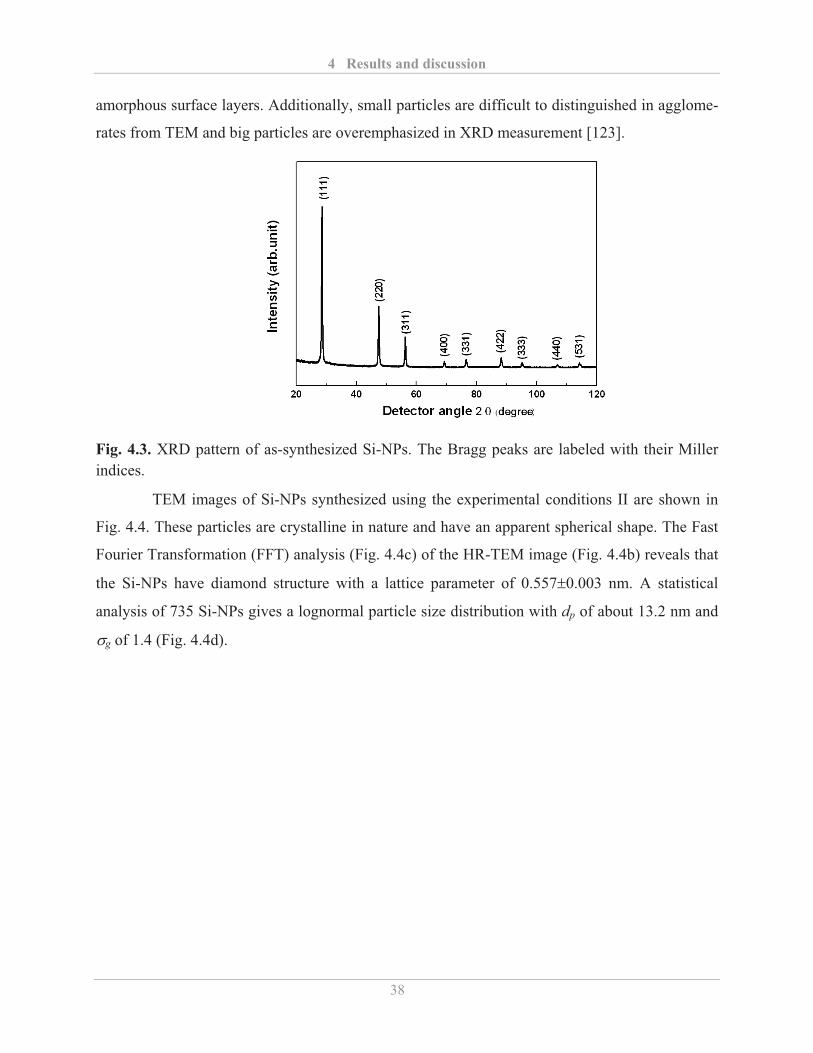
4 Results and discussion
38
amorphous surface layers. Additionally, small particles are difficult to distinguished in agglome-
rates from TEM and big particles are overemphasized in XRD measurement [123].
Fig. 4.3. XRD pattern of as-synthesized Si-NPs. The Bragg peaks are labeled with their Miller indices.
TEM images of Si-NPs synthesized using the experimental conditions II are shown in
Fig. 4.4. These particles are crystalline in nature and have an apparent spherical shape. The Fast
Fourier Transformation (FFT) analysis (Fig. 4.4c) of the HR-TEM image (Fig. 4.4b) reveals that
the Si-NPs have diamond structure with a lattice parameter of 0.557#0.003 nm. A statistical
analysis of 735 Si-NPs gives a lognormal particle size distribution with dp of about 13.2 nm and
�g of 1.4 (Fig. 4.4d).
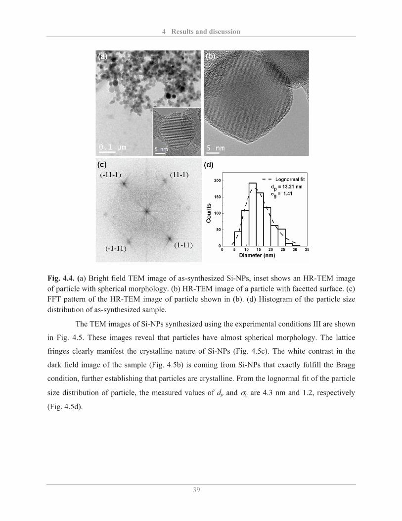
4 Results and discussion
39
Fig. 4.4. (a) Bright field TEM image of as-synthesized Si-NPs, inset shows an HR-TEM image of particle with spherical morphology. (b) HR-TEM image of a particle with facetted surface. (c) FFT pattern of the HR-TEM image of particle shown in (b). (d) Histogram of the particle size distribution of as-synthesized sample.
The TEM images of Si-NPs synthesized using the experimental conditions III are shown
in Fig. 4.5. These images reveal that particles have almost spherical morphology. The lattice
fringes clearly manifest the crystalline nature of Si-NPs (Fig. 4.5c). The white contrast in the
dark field image of the sample (Fig. 4.5b) is coming from Si-NPs that exactly fulfill the Bragg
condition, further establishing that particles are crystalline. From the lognormal fit of the particle
size distribution of particle, the measured values of dp and �g are 4.3 nm and 1.2, respectively
(Fig. 4.5d).
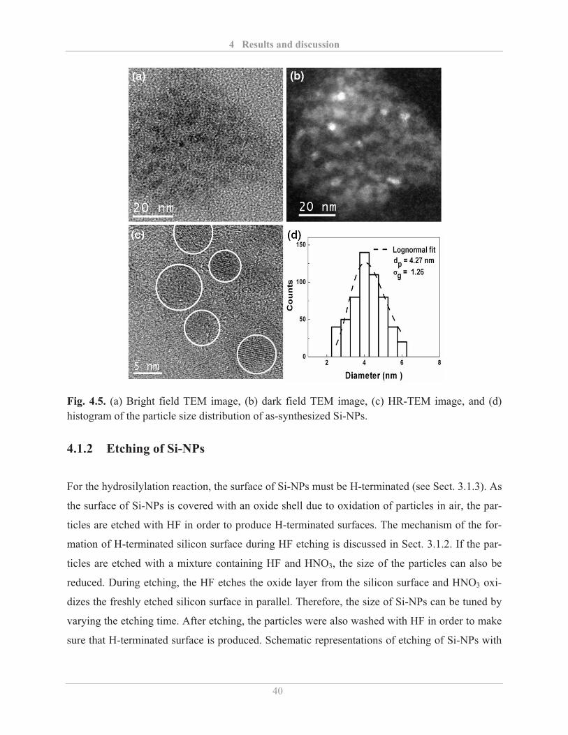
4 Results and discussion
40
Fig. 4.5. (a) Bright field TEM image, (b) dark field TEM image, (c) HR-TEM image, and (d) histogram of the particle size distribution of as-synthesized Si-NPs.
4.1.2 Etching of Si-NPs
For the hydrosilylation reaction, the surface of Si-NPs must be H-terminated (see Sect. 3.1.3). As
the surface of Si-NPs is covered with an oxide shell due to oxidation of particles in air, the par-
ticles are etched with HF in order to produce H-terminated surfaces. The mechanism of the for-
mation of H-terminated silicon surface during HF etching is discussed in Sect. 3.1.2. If the par-
ticles are etched with a mixture containing HF and HNO3, the size of the particles can also be
reduced. During etching, the HF etches the oxide layer from the silicon surface and HNO3 oxi-
dizes the freshly etched silicon surface in parallel. Therefore, the size of Si-NPs can be tuned by
varying the etching time. After etching, the particles were also washed with HF in order to make
sure that H-terminated surface is produced. Schematic representations of etching of Si-NPs with
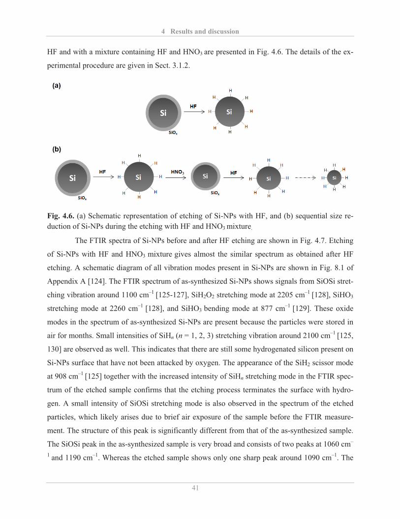
4 Results and discussion
41
HF and with a mixture containing HF and HNO3 are presented in Fig. 4.6. The details of the ex-
perimental procedure are given in Sect. 3.1.2.
Fig. 4.6. (a) Schematic representation of etching of Si-NPs with HF, and (b) sequential size re-duction of Si-NPs during the etching with HF and HNO3 mixture.
The FTIR spectra of Si-NPs before and after HF etching are shown in Fig. 4.7. Etching
of Si-NPs with HF and HNO3 mixture gives almost the similar spectrum as obtained after HF
etching. A schematic diagram of all vibration modes present in Si-NPs are shown in Fig. 8.1 of
Appendix A [124]. The FTIR spectrum of as-synthesized Si-NPs shows signals from SiOSi stret-
ching vibration around 1100 cm–1 [125-127], SiH2O2 stretching mode at 2205 cm–1 [128], SiHO3
stretching mode at 2260 cm–1 [128], and SiHO3 bending mode at 877 cm–1 [129]. These oxide
modes in the spectrum of as-synthesized Si-NPs are present because the particles were stored in
air for months. Small intensities of SiHn (n = 1, 2, 3) stretching vibration around 2100 cm–1 [125,
130] are observed as well. This indicates that there are still some hydrogenated silicon present on
Si-NPs surface that have not been attacked by oxygen. The appearance of the SiH2 scissor mode
at 908 cm–1 [125] together with the increased intensity of SiHn stretching mode in the FTIR spec-
trum of the etched sample confirms that the etching process terminates the surface with hydro-
gen. A small intensity of SiOSi stretching mode is also observed in the spectrum of the etched
particles, which likely arises due to brief air exposure of the sample before the FTIR measure-
ment. The structure of this peak is significantly different from that of the as-synthesized sample.
The SiOSi peak in the as-synthesized sample is very broad and consists of two peaks at 1060 cm–
1 and 1190 cm–1. Whereas the etched sample shows only one sharp peak around 1090 cm–1. The
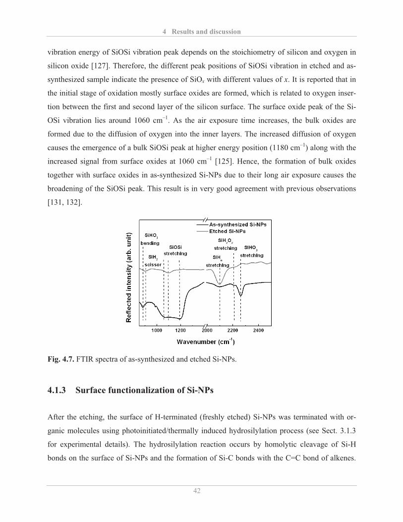
4 Results and discussion
42
vibration energy of SiOSi vibration peak depends on the stoichiometry of silicon and oxygen in
silicon oxide [127]. Therefore, the different peak positions of SiOSi vibration in etched and as-
synthesized sample indicate the presence of SiOx with different values of x. It is reported that in
the initial stage of oxidation mostly surface oxides are formed, which is related to oxygen inser-
tion between the first and second layer of the silicon surface. The surface oxide peak of the Si-
OSi vibration lies around 1060 cm–1. As the air exposure time increases, the bulk oxides are
formed due to the diffusion of oxygen into the inner layers. The increased diffusion of oxygen
causes the emergence of a bulk SiOSi peak at higher energy position (1180 cm–1) along with the
increased signal from surface oxides at 1060 cm–1 [125]. Hence, the formation of bulk oxides
together with surface oxides in as-synthesized Si-NPs due to their long air exposure causes the
broadening of the SiOSi peak. This result is in very good agreement with previous observations
[131, 132].
Fig. 4.7. FTIR spectra of as-synthesized and etched Si-NPs.
4.1.3 Surface functionalization of Si-NPs
After the etching, the surface of H-terminated (freshly etched) Si-NPs was terminated with or-
ganic molecules using photoinitiated/thermally induced hydrosilylation process (see Sect. 3.1.3
for experimental details). The hydrosilylation reaction occurs by homolytic cleavage of Si-H
bonds on the surface of Si-NPs and the formation of Si-C bonds with the C=C bond of alkenes.
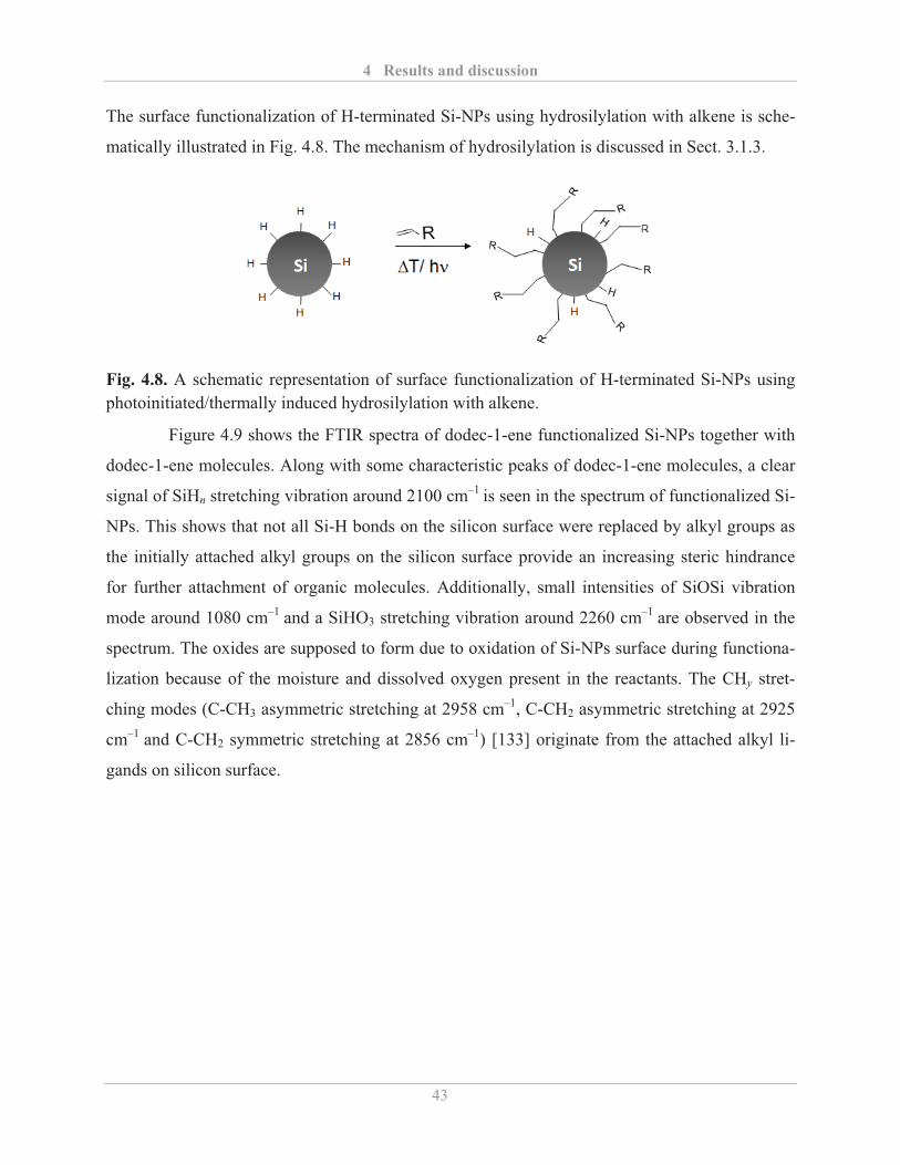
4 Results and discussion
43
The surface functionalization of H-terminated Si-NPs using hydrosilylation with alkene is sche-
matically illustrated in Fig. 4.8. The mechanism of hydrosilylation is discussed in Sect. 3.1.3.
Fig. 4.8. A schematic representation of surface functionalization of H-terminated Si-NPs using photoinitiated/thermally induced hydrosilylation with alkene.
Figure 4.9 shows the FTIR spectra of dodec-1-ene functionalized Si-NPs together with
dodec-1-ene molecules. Along with some characteristic peaks of dodec-1-ene molecules, a clear
signal of SiHn stretching vibration around 2100 cm–1 is seen in the spectrum of functionalized Si-
NPs. This shows that not all Si-H bonds on the silicon surface were replaced by alkyl groups as
the initially attached alkyl groups on the silicon surface provide an increasing steric hindrance
for further attachment of organic molecules. Additionally, small intensities of SiOSi vibration
mode around 1080 cm–1 and a SiHO3 stretching vibration around 2260 cm–1 are observed in the
spectrum. The oxides are supposed to form due to oxidation of Si-NPs surface during functiona-
lization because of the moisture and dissolved oxygen present in the reactants. The CHy stret-
ching modes (C-CH3 asymmetric stretching at 2958 cm–1, C-CH2 asymmetric stretching at 2925
cm–1 and C-CH2 symmetric stretching at 2856 cm–1) [133] originate from the attached alkyl li-
gands on silicon surface.
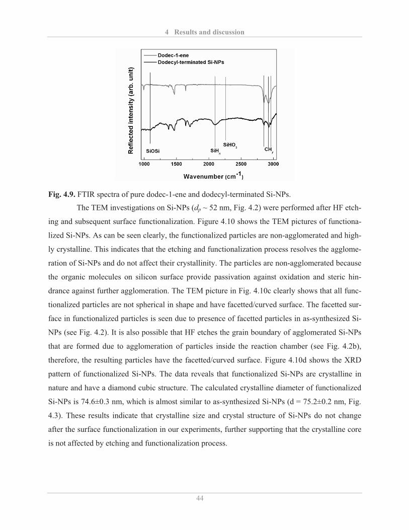
4 Results and discussion
44
Fig. 4.9. FTIR spectra of pure dodec-1-ene and dodecyl-terminated Si-NPs.
The TEM investigations on Si-NPs (dp ~ 52 nm, Fig. 4.2) were performed after HF etch-
ing and subsequent surface functionalization. Figure 4.10 shows the TEM pictures of functiona-
lized Si-NPs. As can be seen clearly, the functionalized particles are non-agglomerated and high-
ly crystalline. This indicates that the etching and functionalization process resolves the agglome-
ration of Si-NPs and do not affect their crystallinity. The particles are non-agglomerated because
the organic molecules on silicon surface provide passivation against oxidation and steric hin-
drance against further agglomeration. The TEM picture in Fig. 4.10c clearly shows that all func-
tionalized particles are not spherical in shape and have facetted/curved surface. The facetted sur-
face in functionalized particles is seen due to presence of facetted particles in as-synthesized Si-
NPs (see Fig. 4.2). It is also possible that HF etches the grain boundary of agglomerated Si-NPs
that are formed due to agglomeration of particles inside the reaction chamber (see Fig. 4.2b),
therefore, the resulting particles have the facetted/curved surface. Figure 4.10d shows the XRD
pattern of functionalized Si-NPs. The data reveals that functionalized Si-NPs are crystalline in
nature and have a diamond cubic structure. The calculated crystalline diameter of functionalized
Si-NPs is 74.6±0.3 nm, which is almost similar to as-synthesized Si-NPs (d = 75.2±0.2 nm, Fig.
4.3). These results indicate that crystalline size and crystal structure of Si-NPs do not change
after the surface functionalization in our experiments, further supporting that the crystalline core
is not affected by etching and functionalization process.
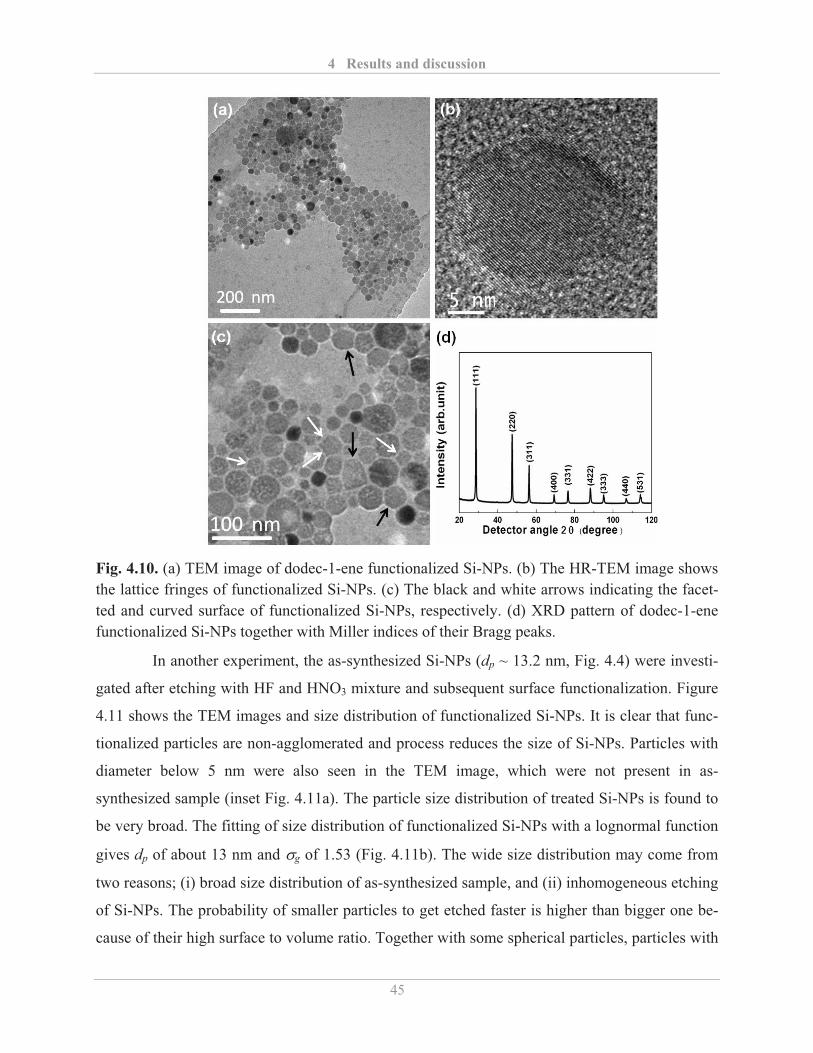
4 Results and discussion
45
Fig. 4.10. (a) TEM image of dodec-1-ene functionalized Si-NPs. (b) The HR-TEM image shows the lattice fringes of functionalized Si-NPs. (c) The black and white arrows indicating the facet-ted and curved surface of functionalized Si-NPs, respectively. (d) XRD pattern of dodec-1-ene functionalized Si-NPs together with Miller indices of their Bragg peaks.
In another experiment, the as-synthesized Si-NPs (dp ~ 13.2 nm, Fig. 4.4) were investi-
gated after etching with HF and HNO3 mixture and subsequent surface functionalization. Figure
4.11 shows the TEM images and size distribution of functionalized Si-NPs. It is clear that func-
tionalized particles are non-agglomerated and process reduces the size of Si-NPs. Particles with
diameter below 5 nm were also seen in the TEM image, which were not present in as-
synthesized sample (inset Fig. 4.11a). The particle size distribution of treated Si-NPs is found to
be very broad. The fitting of size distribution of functionalized Si-NPs with a lognormal function
gives dp of about 13 nm and �g of 1.53 (Fig. 4.11b). The wide size distribution may come from
two reasons; (i) broad size distribution of as-synthesized sample, and (ii) inhomogeneous etching
of Si-NPs. The probability of smaller particles to get etched faster is higher than bigger one be-
cause of their high surface to volume ratio. Together with some spherical particles, particles with
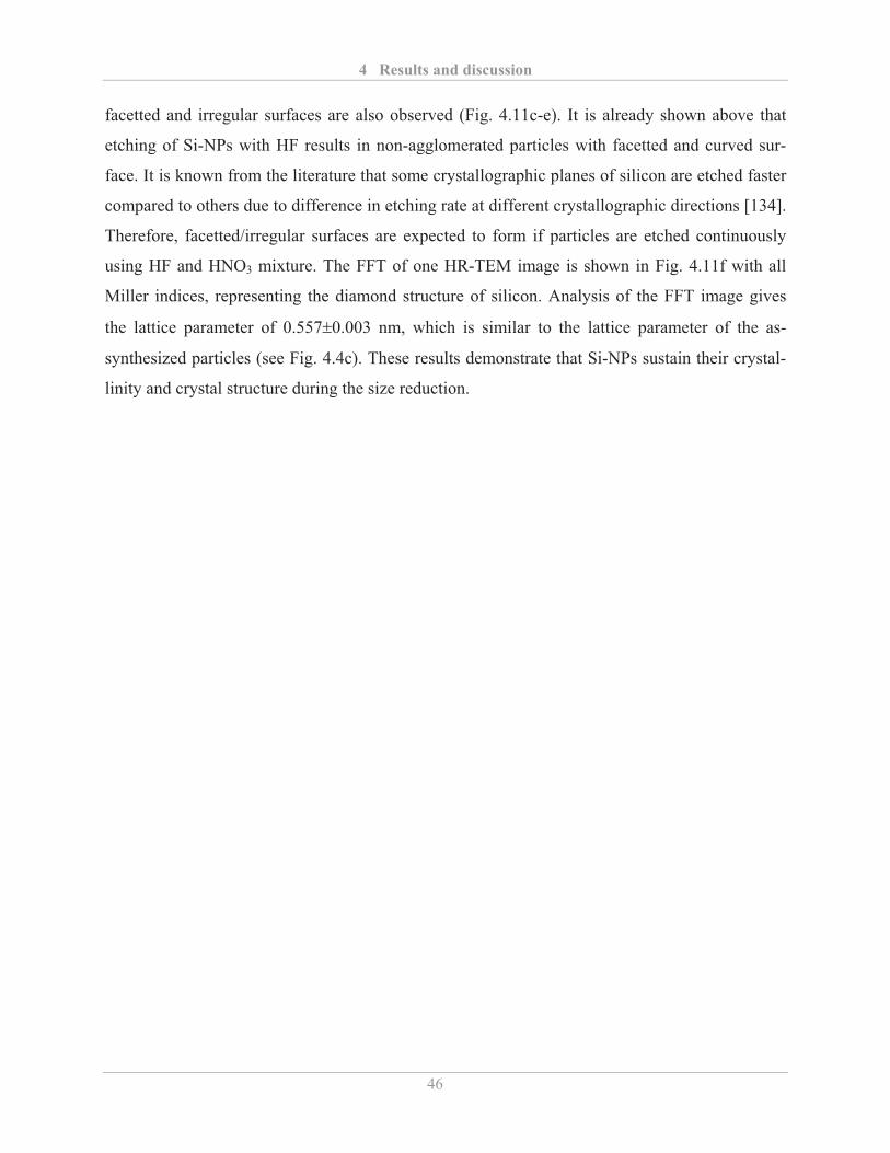
4 Results and discussion
46
facetted and irregular surfaces are also observed (Fig. 4.11c-e). It is already shown above that
etching of Si-NPs with HF results in non-agglomerated particles with facetted and curved sur-
face. It is known from the literature that some crystallographic planes of silicon are etched faster
compared to others due to difference in etching rate at different crystallographic directions [134].
Therefore, facetted/irregular surfaces are expected to form if particles are etched continuously
using HF and HNO3 mixture. The FFT of one HR-TEM image is shown in Fig. 4.11f with all
Miller indices, representing the diamond structure of silicon. Analysis of the FFT image gives
the lattice parameter of 0.557#0.003 nm, which is similar to the lattice parameter of the as-
synthesized particles (see Fig. 4.4c). These results demonstrate that Si-NPs sustain their crystal-
linity and crystal structure during the size reduction.
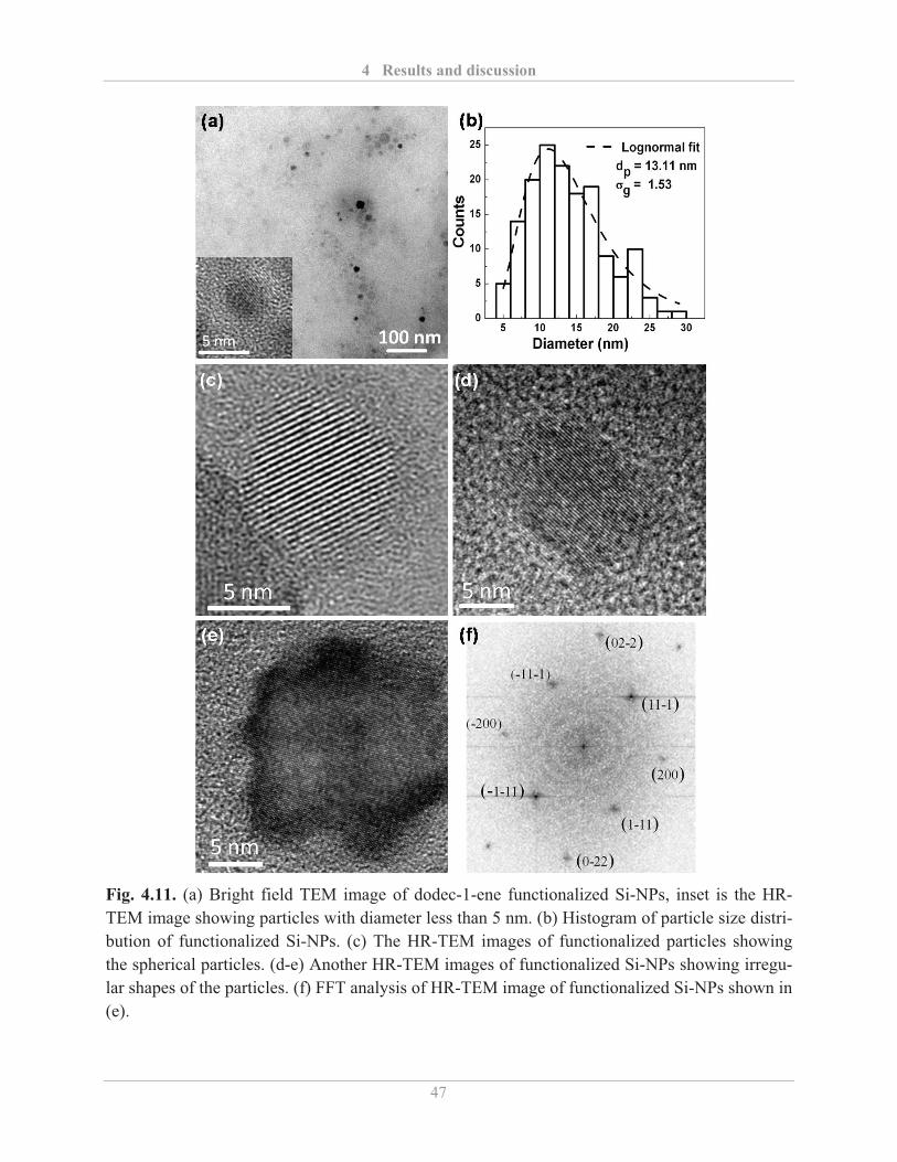
4 Results and discussion
47
Fig. 4.11. (a) Bright field TEM image of dodec-1-ene functionalized Si-NPs, inset is the HR-TEM image showing particles with diameter less than 5 nm. (b) Histogram of particle size distri-bution of functionalized Si-NPs. (c) The HR-TEM images of functionalized particles showing the spherical particles. (d-e) Another HR-TEM images of functionalized Si-NPs showing irregu-lar shapes of the particles. (f) FFT analysis of HR-TEM image of functionalized Si-NPs shown in (e).
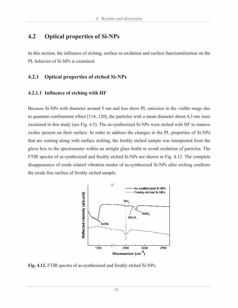
4 Results and discussion
48
4.2 Optical properties of Si-NPs
In this section, the influence of etching, surface re-oxidation and surface functionalization on the
PL behavior of Si-NPs is examined.
4.2.1 Optical properties of etched Si-NPs
4.2.1.1 Influence of etching with HF
Because Si-NPs with diameter around 5 nm and less show PL emission in the visible range due
to quantum confinement effect [114, 120], the particles with a mean diameter about 4.3 nm were
examined in this study (see Fig. 4.5). The as-synthesized Si-NPs were etched with HF to remove
oxides present on their surface. In order to address the changes in the PL properties of Si-NPs
that are coming along with surface etching, the freshly etched sample was transported from the
glove box to the spectrometer within an airtight glass bottle to avoid oxidation of particles. The
FTIR spectra of as-synthesized and freshly etched Si-NPs are shown in Fig. 4.12. The complete
disappearance of oxide related vibration modes of as-synthesized Si-NPs after etching confirms
the oxide free surface of freshly etched sample.
Fig. 4.12. FTIR spectra of as-synthesized and freshly etched Si-NPs.
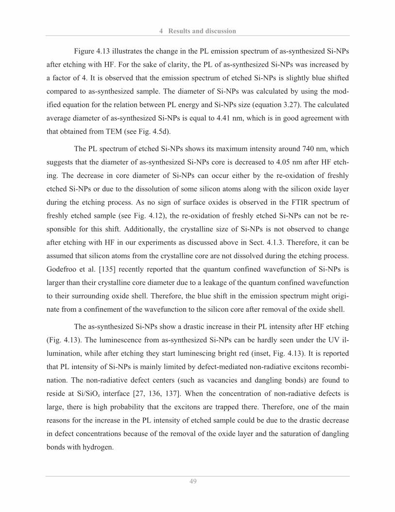
4 Results and discussion
49
Figure 4.13 illustrates the change in the PL emission spectrum of as-synthesized Si-NPs
after etching with HF. For the sake of clarity, the PL of as-synthesized Si-NPs was increased by
a factor of 4. It is observed that the emission spectrum of etched Si-NPs is slightly blue shifted
compared to as-synthesized sample. The diameter of Si-NPs was calculated by using the mod-
ified equation for the relation between PL energy and Si-NPs size (equation 3.27). The calculated
average diameter of as-synthesized Si-NPs is equal to 4.41 nm, which is in good agreement with
that obtained from TEM (see Fig. 4.5d).
The PL spectrum of etched Si-NPs shows its maximum intensity around 740 nm, which
suggests that the diameter of as-synthesized Si-NPs core is decreased to 4.05 nm after HF etch-
ing. The decrease in core diameter of Si-NPs can occur either by the re-oxidation of freshly
etched Si-NPs or due to the dissolution of some silicon atoms along with the silicon oxide layer
during the etching process. As no sign of surface oxides is observed in the FTIR spectrum of
freshly etched sample (see Fig. 4.12), the re-oxidation of freshly etched Si-NPs can not be re-
sponsible for this shift. Additionally, the crystalline size of Si-NPs is not observed to change
after etching with HF in our experiments as discussed above in Sect. 4.1.3. Therefore, it can be
assumed that silicon atoms from the crystalline core are not dissolved during the etching process.
Godefroo et al. [135] recently reported that the quantum confined wavefunction of Si-NPs is
larger than their crystalline core diameter due to a leakage of the quantum confined wavefunction
to their surrounding oxide shell. Therefore, the blue shift in the emission spectrum might origi-
nate from a confinement of the wavefunction to the silicon core after removal of the oxide shell.
The as-synthesized Si-NPs show a drastic increase in their PL intensity after HF etching
(Fig. 4.13). The luminescence from as-synthesized Si-NPs can be hardly seen under the UV il-
lumination, while after etching they start luminescing bright red (inset, Fig. 4.13). It is reported
that PL intensity of Si-NPs is mainly limited by defect-mediated non-radiative excitons recombi-
nation. The non-radiative defect centers (such as vacancies and dangling bonds) are found to
reside at Si/SiOx interface [27, 136, 137]. When the concentration of non-radiative defects is
large, there is high probability that the excitons are trapped there. Therefore, one of the main
reasons for the increase in the PL intensity of etched sample could be due to the drastic decrease
in defect concentrations because of the removal of the oxide layer and the saturation of dangling
bonds with hydrogen.
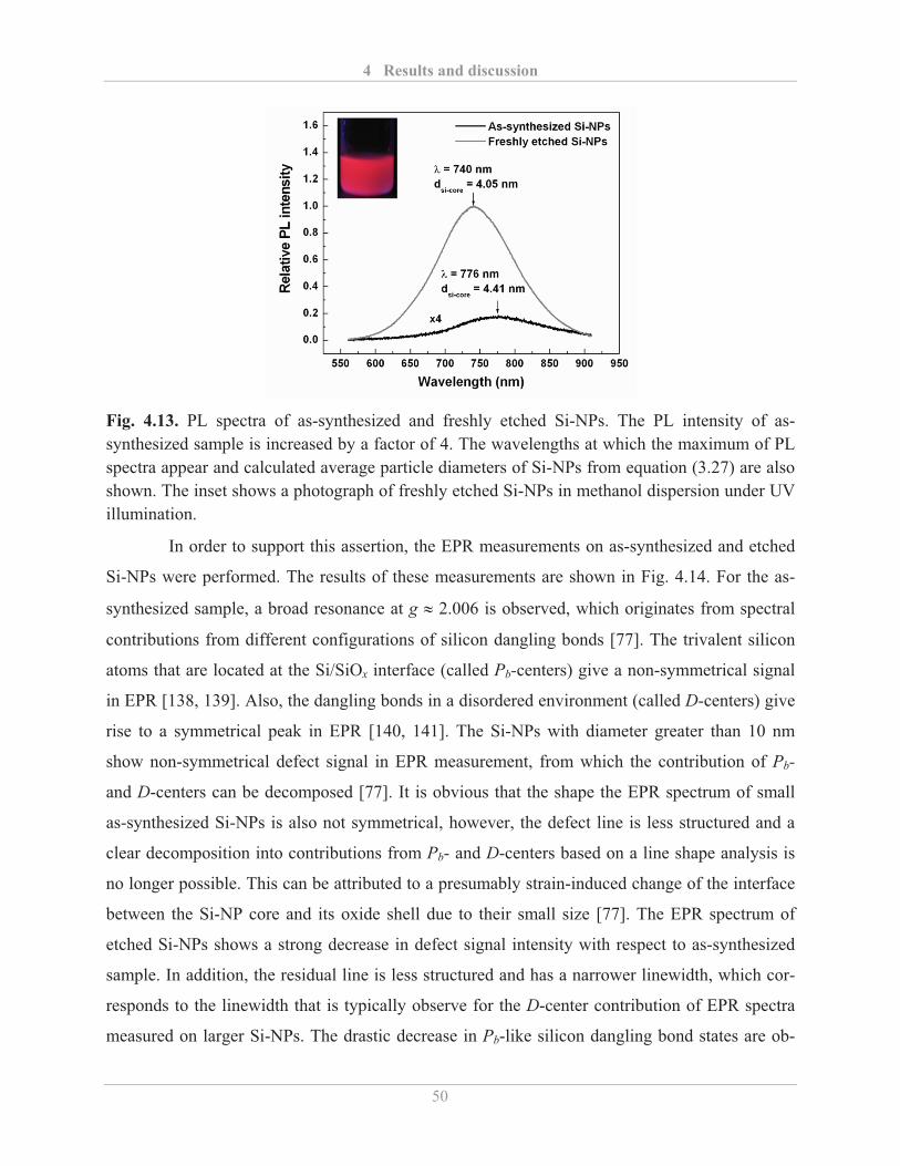
4 Results and discussion
50
Fig. 4.13. PL spectra of as-synthesized and freshly etched Si-NPs. The PL intensity of as-synthesized sample is increased by a factor of 4. The wavelengths at which the maximum of PL spectra appear and calculated average particle diameters of Si-NPs from equation (3.27) are also shown. The inset shows a photograph of freshly etched Si-NPs in methanol dispersion under UV illumination.
In order to support this assertion, the EPR measurements on as-synthesized and etched
Si-NPs were performed. The results of these measurements are shown in Fig. 4.14. For the as-
synthesized sample, a broad resonance at g � 2.006 is observed, which originates from spectral
contributions from different configurations of silicon dangling bonds [77]. The trivalent silicon
atoms that are located at the Si/SiOx interface (called Pb-centers) give a non-symmetrical signal
in EPR [138, 139]. Also, the dangling bonds in a disordered environment (called D-centers) give
rise to a symmetrical peak in EPR [140, 141]. The Si-NPs with diameter greater than 10 nm
show non-symmetrical defect signal in EPR measurement, from which the contribution of Pb-
and D-centers can be decomposed [77]. It is obvious that the shape the EPR spectrum of small
as-synthesized Si-NPs is also not symmetrical, however, the defect line is less structured and a
clear decomposition into contributions from Pb- and D-centers based on a line shape analysis is
no longer possible. This can be attributed to a presumably strain-induced change of the interface
between the Si-NP core and its oxide shell due to their small size [77]. The EPR spectrum of
etched Si-NPs shows a strong decrease in defect signal intensity with respect to as-synthesized
sample. In addition, the residual line is less structured and has a narrower linewidth, which cor-
responds to the linewidth that is typically observe for the D-center contribution of EPR spectra
measured on larger Si-NPs. The drastic decrease in Pb-like silicon dangling bond states are ob-
4 Results and discussion
51
served due to the removal of the oxide layer and the saturation of dangling bonds with hydrogen.
The residual defect signal measured after HF etching is attributed to D-centers present in a sub-
ensemble of Si-NPs with amorphous contributions. Thus, the drastic decrease in PL intensity of
Si-NPs after HF etching can be significantly related to the decrease in of overall defects concen-
tration.
Fig. 4.14. EPR spectra of as-synthesized and etched Si-NPs.
4.2.1.2 Influence of etching with HF and HNO3
In order to see the size dependent PL, the size of Si-NPs (dp ~ 4.3 nm, Fig. 4.5) is reduced by
etching them in a mixture containing HF and HNO3. Different samples were prepared at various
etching time. After the etching, the samples were washed with HF in order to make sure that no
surface oxides remains on the surface. Figure 4.15a depicts the PL spectra recorded from differ-
ent etched samples. It is clear that Si-NPs show a continuous blue shift in their emission spectra
with increasing etching time. According to the quantum confinement model, the PL from Si-NPs
blue shifts when the size of Si-NPs decreases [32, 114, 142-144]. Therefore, the blue shift in the
emission spectra can be reliably correlated to the size reduction of Si-NPs during etching. It is
observed that the color of emitted light evolves from red (731 nm) to green (556 nm) during the
etching process (Fig. 4.15a,b), thereby endorsing the origin of red to green PL from the quantum
confinement effects.
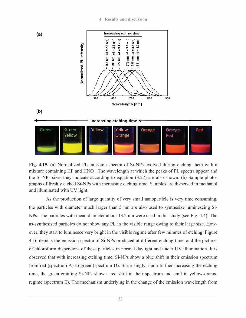
4 Results and discussion
52
Fig. 4.15. (a) Normalized PL emission spectra of Si-NPs evolved during etching them with a mixture containing HF and HNO3. The wavelength at which the peaks of PL spectra appear and the Si-NPs sizes they indicate according to equation (3.27) are also shown. (b) Sample photo-graphs of freshly etched Si-NPs with increasing etching time. Samples are dispersed in methanol and illuminated with UV light.
As the production of large quantity of very small nanoparticle is very time consuming,
the particles with diameter much larger than 5 nm are also used to synthesize luminescing Si-
NPs. The particles with mean diameter about 13.2 nm were used in this study (see Fig. 4.4). The
as-synthesized particles do not show any PL in the visible range owing to their large size. How-
ever, they start to luminesce very bright in the visible regime after few minutes of etching. Figure
4.16 depicts the emission spectra of Si-NPs produced at different etching time, and the pictures
of chloroform dispersions of these particles in normal daylight and under UV illumination. It is
observed that with increasing etching time, Si-NPs show a blue shift in their emission spectrum
from red (spectrum A) to green (spectrum D). Surprisingly, upon further increasing the etching
time, the green emitting Si-NPs show a red shift in their spectrum and emit in yellow-orange
regime (spectrum E). The mechanism underlying in the change of the emission wavelength from
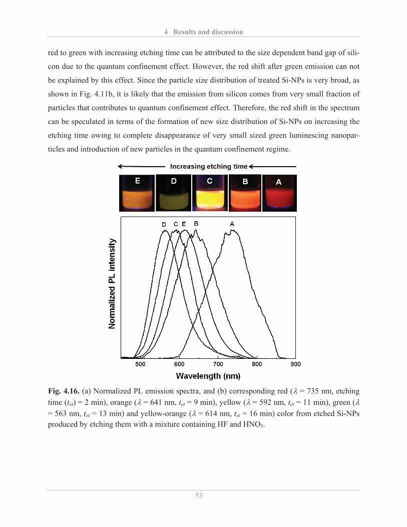
4 Results and discussion
53
red to green with increasing etching time can be attributed to the size dependent band gap of sili-
con due to the quantum confinement effect. However, the red shift after green emission can not
be explained by this effect. Since the particle size distribution of treated Si-NPs is very broad, as
shown in Fig. 4.11b, it is likely that the emission from silicon comes from very small fraction of
particles that contributes to quantum confinement effect. Therefore, the red shift in the spectrum
can be speculated in terms of the formation of new size distribution of Si-NPs on increasing the
etching time owing to complete disappearance of very small sized green luminescing nanopar-
ticles and introduction of new particles in the quantum confinement regime.
Fig. 4.16. (a) Normalized PL emission spectra, and (b) corresponding red (� = 735 nm, etching time (tet) = 2 min), orange (� = 641 nm, tet = 9 min), yellow (� = 592 nm, tet = 11 min), green (� = 563 nm, tet = 13 min) and yellow-orange (� = 614 nm, tet = 16 min) color from etched Si-NPs produced by etching them with a mixture containing HF and HNO3.
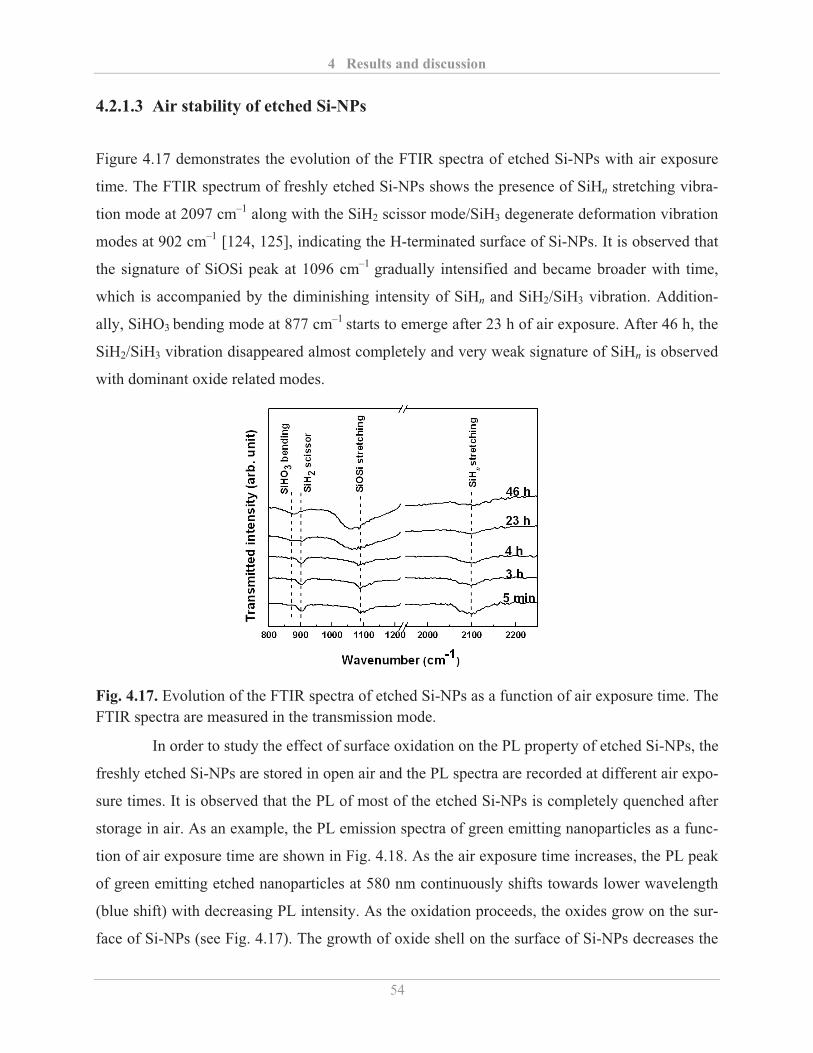
4 Results and discussion
54
4.2.1.3 Air stability of etched Si-NPs
Figure 4.17 demonstrates the evolution of the FTIR spectra of etched Si-NPs with air exposure
time. The FTIR spectrum of freshly etched Si-NPs shows the presence of SiHn stretching vibra-
tion mode at 2097 cm–1 along with the SiH2 scissor mode/SiH3 degenerate deformation vibration
modes at 902 cm–1 [124, 125], indicating the H-terminated surface of Si-NPs. It is observed that
the signature of SiOSi peak at 1096 cm–1 gradually intensified and became broader with time,
which is accompanied by the diminishing intensity of SiHn and SiH2/SiH3 vibration. Addition-
ally, SiHO3 bending mode at 877 cm–1 starts to emerge after 23 h of air exposure. After 46 h, the
SiH2/SiH3 vibration disappeared almost completely and very weak signature of SiHn is observed
with dominant oxide related modes.
Fig. 4.17. Evolution of the FTIR spectra of etched Si-NPs as a function of air exposure time. The FTIR spectra are measured in the transmission mode.
In order to study the effect of surface oxidation on the PL property of etched Si-NPs, the
freshly etched Si-NPs are stored in open air and the PL spectra are recorded at different air expo-
sure times. It is observed that the PL of most of the etched Si-NPs is completely quenched after
storage in air. As an example, the PL emission spectra of green emitting nanoparticles as a func-
tion of air exposure time are shown in Fig. 4.18. As the air exposure time increases, the PL peak
of green emitting etched nanoparticles at 580 nm continuously shifts towards lower wavelength
(blue shift) with decreasing PL intensity. As the oxidation proceeds, the oxides grow on the sur-
face of Si-NPs (see Fig. 4.17). The growth of oxide shell on the surface of Si-NPs decreases the
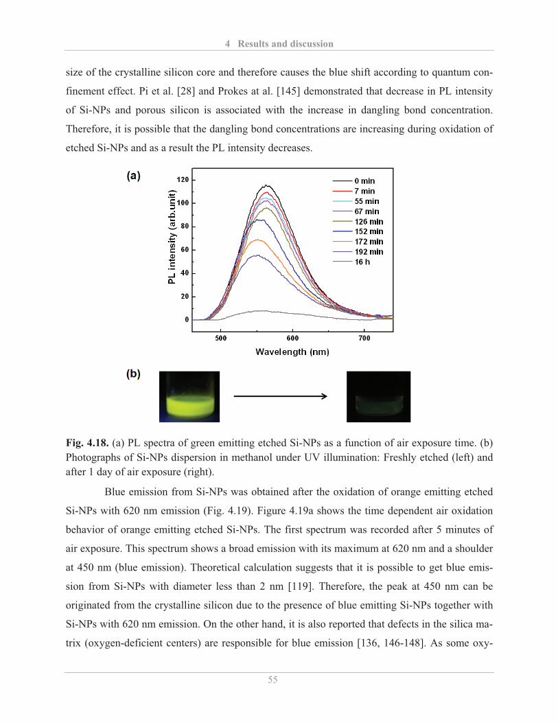
4 Results and discussion
55
size of the crystalline silicon core and therefore causes the blue shift according to quantum con-
finement effect. Pi et al. [28] and Prokes at al. [145] demonstrated that decrease in PL intensity
of Si-NPs and porous silicon is associated with the increase in dangling bond concentration.
Therefore, it is possible that the dangling bond concentrations are increasing during oxidation of
etched Si-NPs and as a result the PL intensity decreases.
Fig. 4.18. (a) PL spectra of green emitting etched Si-NPs as a function of air exposure time. (b) Photographs of Si-NPs dispersion in methanol under UV illumination: Freshly etched (left) and after 1 day of air exposure (right).
Blue emission from Si-NPs was obtained after the oxidation of orange emitting etched
Si-NPs with 620 nm emission (Fig. 4.19). Figure 4.19a shows the time dependent air oxidation
behavior of orange emitting etched Si-NPs. The first spectrum was recorded after 5 minutes of
air exposure. This spectrum shows a broad emission with its maximum at 620 nm and a shoulder
at 450 nm (blue emission). Theoretical calculation suggests that it is possible to get blue emis-
sion from Si-NPs with diameter less than 2 nm [119]. Therefore, the peak at 450 nm can be
originated from the crystalline silicon due to the presence of blue emitting Si-NPs together with
Si-NPs with 620 nm emission. On the other hand, it is also reported that defects in the silica ma-
trix (oxygen-deficient centers) are responsible for blue emission [136, 146-148]. As some oxy-
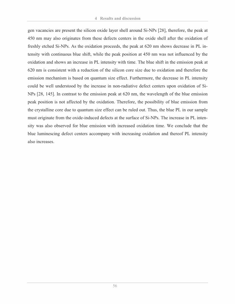
4 Results and discussion
56
gen vacancies are present the silicon oxide layer shell around Si-NPs [28], therefore, the peak at
450 nm may also originates from these defects centers in the oxide shell after the oxidation of
freshly etched Si-NPs. As the oxidation proceeds, the peak at 620 nm shows decrease in PL in-
tensity with continuous blue shift, while the peak position at 450 nm was not influenced by the
oxidation and shows an increase in PL intensity with time. The blue shift in the emission peak at
620 nm is consistent with a reduction of the silicon core size due to oxidation and therefore the
emission mechanism is based on quantum size effect. Furthermore, the decrease in PL intensity
could be well understood by the increase in non-radiative defect centers upon oxidation of Si-
NPs [28, 145]. In contrast to the emission peak at 620 nm, the wavelength of the blue emission
peak position is not affected by the oxidation. Therefore, the possibility of blue emission from
the crystalline core due to quantum size effect can be ruled out. Thus, the blue PL in our sample
must originate from the oxide-induced defects at the surface of Si-NPs. The increase in PL inten-
sity was also observed for blue emission with increased oxidation time. We conclude that the
blue luminescing defect centers accompany with increasing oxidation and thereof PL intensity
also increases.
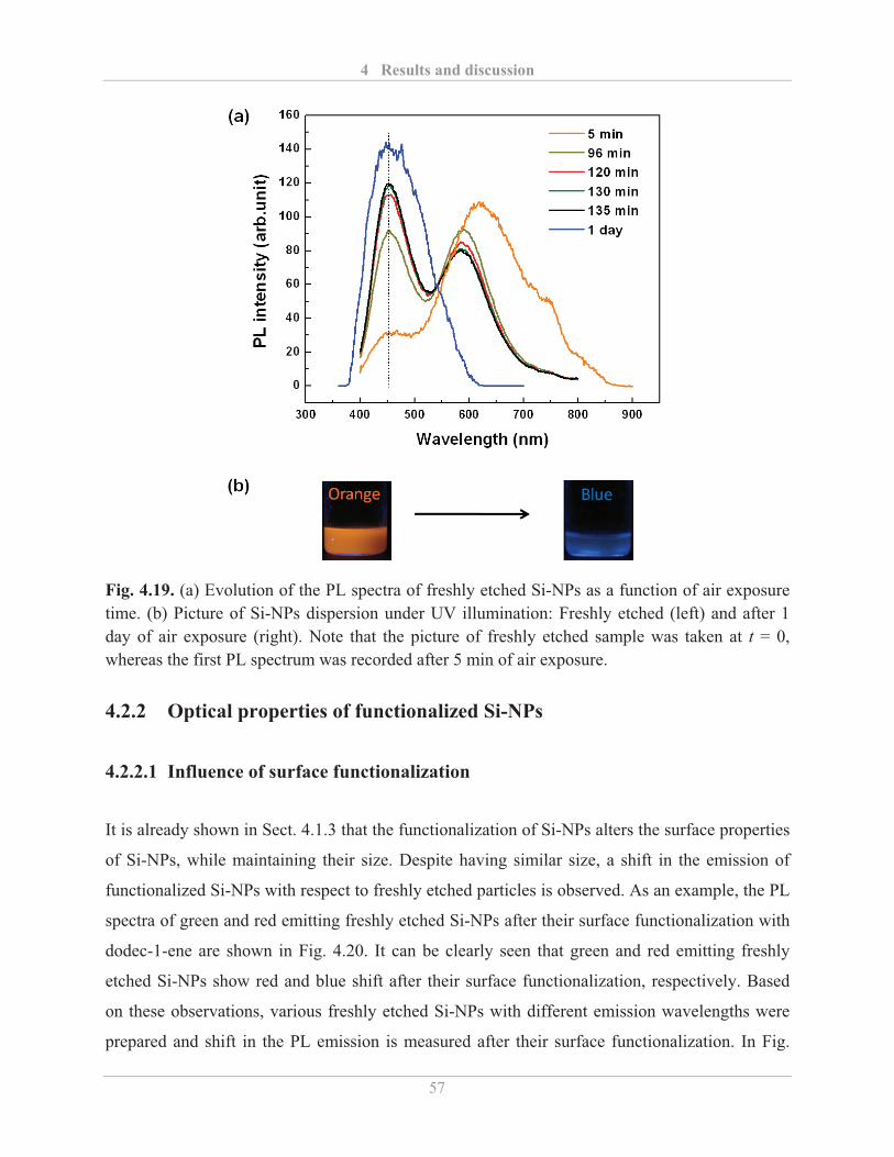
4 Results and discussion
57
Fig. 4.19. (a) Evolution of the PL spectra of freshly etched Si-NPs as a function of air exposure time. (b) Picture of Si-NPs dispersion under UV illumination: Freshly etched (left) and after 1 day of air exposure (right). Note that the picture of freshly etched sample was taken at t = 0, whereas the first PL spectrum was recorded after 5 min of air exposure.
4.2.2 Optical properties of functionalized Si-NPs
4.2.2.1 Influence of surface functionalization
It is already shown in Sect. 4.1.3 that the functionalization of Si-NPs alters the surface properties
of Si-NPs, while maintaining their size. Despite having similar size, a shift in the emission of
functionalized Si-NPs with respect to freshly etched particles is observed. As an example, the PL
spectra of green and red emitting freshly etched Si-NPs after their surface functionalization with
dodec-1-ene are shown in Fig. 4.20. It can be clearly seen that green and red emitting freshly
etched Si-NPs show red and blue shift after their surface functionalization, respectively. Based
on these observations, various freshly etched Si-NPs with different emission wavelengths were
prepared and shift in the PL emission is measured after their surface functionalization. In Fig.
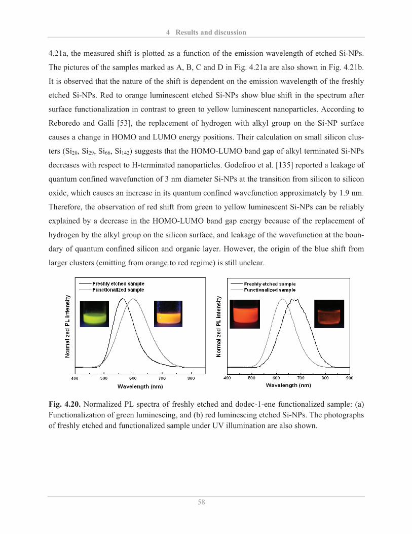
4 Results and discussion
58
4.21a, the measured shift is plotted as a function of the emission wavelength of etched Si-NPs.
The pictures of the samples marked as A, B, C and D in Fig. 4.21a are also shown in Fig. 4.21b.
It is observed that the nature of the shift is dependent on the emission wavelength of the freshly
etched Si-NPs. Red to orange luminescent etched Si-NPs show blue shift in the spectrum after
surface functionalization in contrast to green to yellow luminescent nanoparticles. According to
Reboredo and Galli [53], the replacement of hydrogen with alkyl group on the Si-NP surface
causes a change in HOMO and LUMO energy positions. Their calculation on small silicon clus-
ters (Si20, Si29, Si66, Si142) suggests that the HOMO-LUMO band gap of alkyl terminated Si-NPs
decreases with respect to H-terminated nanoparticles. Godefroo et al. [135] reported a leakage of
quantum confined wavefunction of 3 nm diameter Si-NPs at the transition from silicon to silicon
oxide, which causes an increase in its quantum confined wavefunction approximately by 1.9 nm.
Therefore, the observation of red shift from green to yellow luminescent Si-NPs can be reliably
explained by a decrease in the HOMO-LUMO band gap energy because of the replacement of
hydrogen by the alkyl group on the silicon surface, and leakage of the wavefunction at the boun-
dary of quantum confined silicon and organic layer. However, the origin of the blue shift from
larger clusters (emitting from orange to red regime) is still unclear.
Fig. 4.20. Normalized PL spectra of freshly etched and dodec-1-ene functionalized sample: (a) Functionalization of green luminescing, and (b) red luminescing etched Si-NPs. The photographs of freshly etched and functionalized sample under UV illumination are also shown.
4 Results and discussion
59
Fig. 4.21. (a) Shift in the emission wavelength of freshly etched Si-NPs after surface functionali-zation. (b) Sample photographs of freshly etched (at the tail of arrow) and functionalized (at the head of arrow) Si-NPs under UV illumination, corresponding to A, B, C and D data points of (a), showing change in their emission color.
4.2.2.2 Factors influencing the PL properties of functionalized Si-NPs
It is observed that the magnitude of shift in the emission wavelength of functionalized Si-NPs
with respect to freshly etched sample can be altered. In order to study the factors influencing the
shift, the PL emission of functionalized Si-NPs is measured by varying different reaction para-
meters during the surface functionalization. Note that all the results shown below are obtained
after the surface functionalization of green-yellow emitting etched Si-NPs and in all the cases a
red shift in their PL emission is observed. The PL results shown in one figure can not be com-
pared with the others as the emission wavelength of green-yellow emitting freshly etched sample
is not the same. All the PL measurements were performed using a diode laser with an excitation
wavelength of 405 nm. Therefore, the second harmonic of the excitation wavelength is present as
a sharp signal in the spectra shown below.
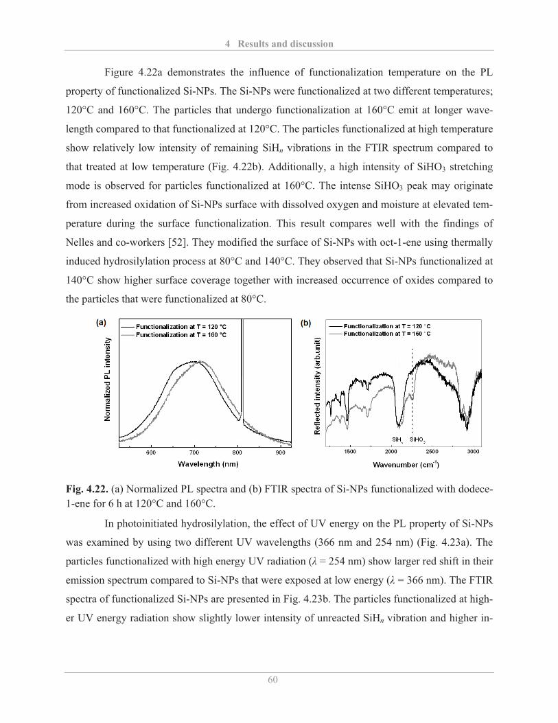
4 Results and discussion
60
Figure 4.22a demonstrates the influence of functionalization temperature on the PL
property of functionalized Si-NPs. The Si-NPs were functionalized at two different temperatures;
120°C and 160°C. The particles that undergo functionalization at 160°C emit at longer wave-
length compared to that functionalized at 120°C. The particles functionalized at high temperature
show relatively low intensity of remaining SiHn vibrations in the FTIR spectrum compared to
that treated at low temperature (Fig. 4.22b). Additionally, a high intensity of SiHO3 stretching
mode is observed for particles functionalized at 160°C. The intense SiHO3 peak may originate
from increased oxidation of Si-NPs surface with dissolved oxygen and moisture at elevated tem-
perature during the surface functionalization. This result compares well with the findings of
Nelles and co-workers [52]. They modified the surface of Si-NPs with oct-1-ene using thermally
induced hydrosilylation process at 80°C and 140°C. They observed that Si-NPs functionalized at
140°C show higher surface coverage together with increased occurrence of oxides compared to
the particles that were functionalized at 80°C.
Fig. 4.22. (a) Normalized PL spectra and (b) FTIR spectra of Si-NPs functionalized with dodece-1-ene for 6 h at 120°C and 160°C.
In photoinitiated hydrosilylation, the effect of UV energy on the PL property of Si-NPs
was examined by using two different UV wavelengths (366 nm and 254 nm) (Fig. 4.23a). The
particles functionalized with high energy UV radiation (� = 254 nm) show larger red shift in their
emission spectrum compared to Si-NPs that were exposed at low energy (� = 366 nm). The FTIR
spectra of functionalized Si-NPs are presented in Fig. 4.23b. The particles functionalized at high-
er UV energy radiation show slightly lower intensity of unreacted SiHn vibration and higher in-
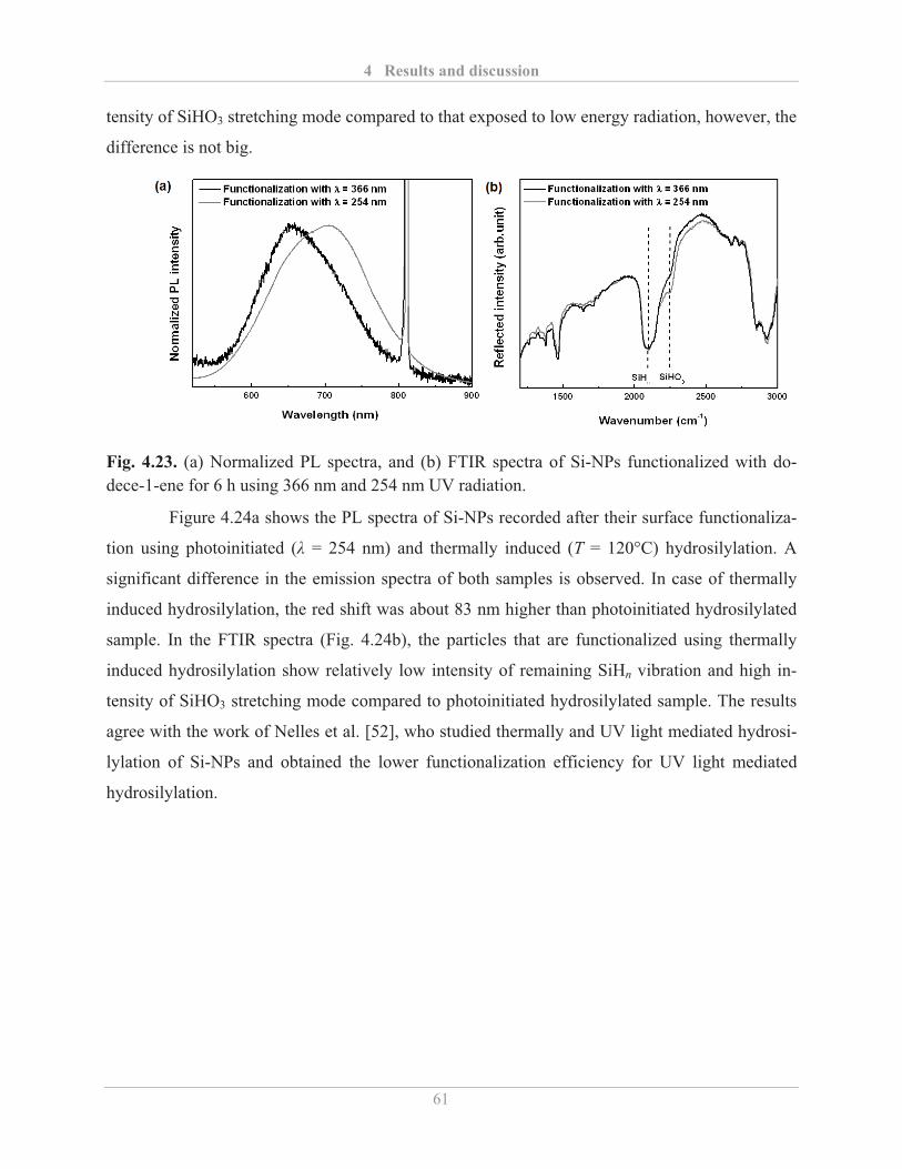
4 Results and discussion
61
tensity of SiHO3 stretching mode compared to that exposed to low energy radiation, however, the
difference is not big.
Fig. 4.23. (a) Normalized PL spectra, and (b) FTIR spectra of Si-NPs functionalized with do-dece-1-ene for 6 h using 366 nm and 254 nm UV radiation.
Figure 4.24a shows the PL spectra of Si-NPs recorded after their surface functionaliza-
tion using photoinitiated (� = 254 nm) and thermally induced (T = 120°C) hydrosilylation. A
significant difference in the emission spectra of both samples is observed. In case of thermally
induced hydrosilylation, the red shift was about 83 nm higher than photoinitiated hydrosilylated
sample. In the FTIR spectra (Fig. 4.24b), the particles that are functionalized using thermally
induced hydrosilylation show relatively low intensity of remaining SiHn vibration and high in-
tensity of SiHO3 stretching mode compared to photoinitiated hydrosilylated sample. The results
agree with the work of Nelles et al. [52], who studied thermally and UV light mediated hydrosi-
lylation of Si-NPs and obtained the lower functionalization efficiency for UV light mediated
hydrosilylation.
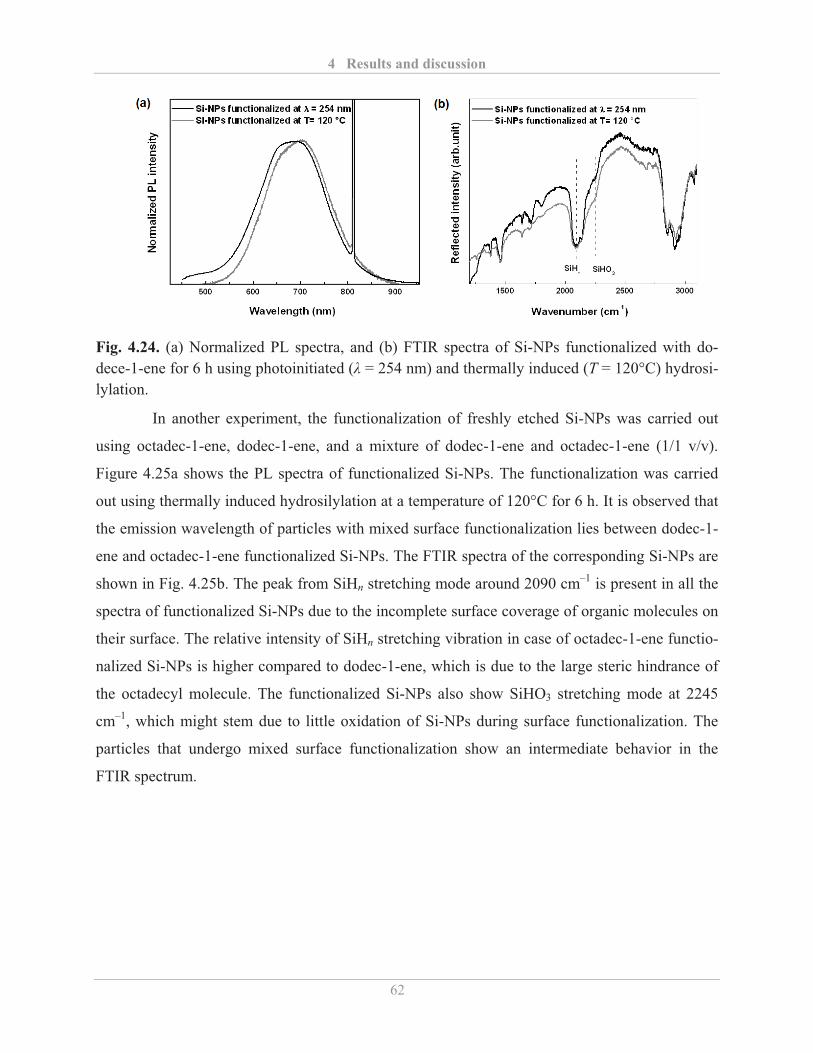
4 Results and discussion
62
Fig. 4.24. (a) Normalized PL spectra, and (b) FTIR spectra of Si-NPs functionalized with do-dece-1-ene for 6 h using photoinitiated (� = 254 nm) and thermally induced (T = 120°C) hydrosi-lylation.
In another experiment, the functionalization of freshly etched Si-NPs was carried out
using octadec-1-ene, dodec-1-ene, and a mixture of dodec-1-ene and octadec-1-ene (1/1 v/v).
Figure 4.25a shows the PL spectra of functionalized Si-NPs. The functionalization was carried
out using thermally induced hydrosilylation at a temperature of 120°C for 6 h. It is observed that
the emission wavelength of particles with mixed surface functionalization lies between dodec-1-
ene and octadec-1-ene functionalized Si-NPs. The FTIR spectra of the corresponding Si-NPs are
shown in Fig. 4.25b. The peak from SiHn stretching mode around 2090 cm–1 is present in all the
spectra of functionalized Si-NPs due to the incomplete surface coverage of organic molecules on
their surface. The relative intensity of SiHn stretching vibration in case of octadec-1-ene functio-
nalized Si-NPs is higher compared to dodec-1-ene, which is due to the large steric hindrance of
the octadecyl molecule. The functionalized Si-NPs also show SiHO3 stretching mode at 2245
cm–1, which might stem due to little oxidation of Si-NPs during surface functionalization. The
particles that undergo mixed surface functionalization show an intermediate behavior in the
FTIR spectrum.
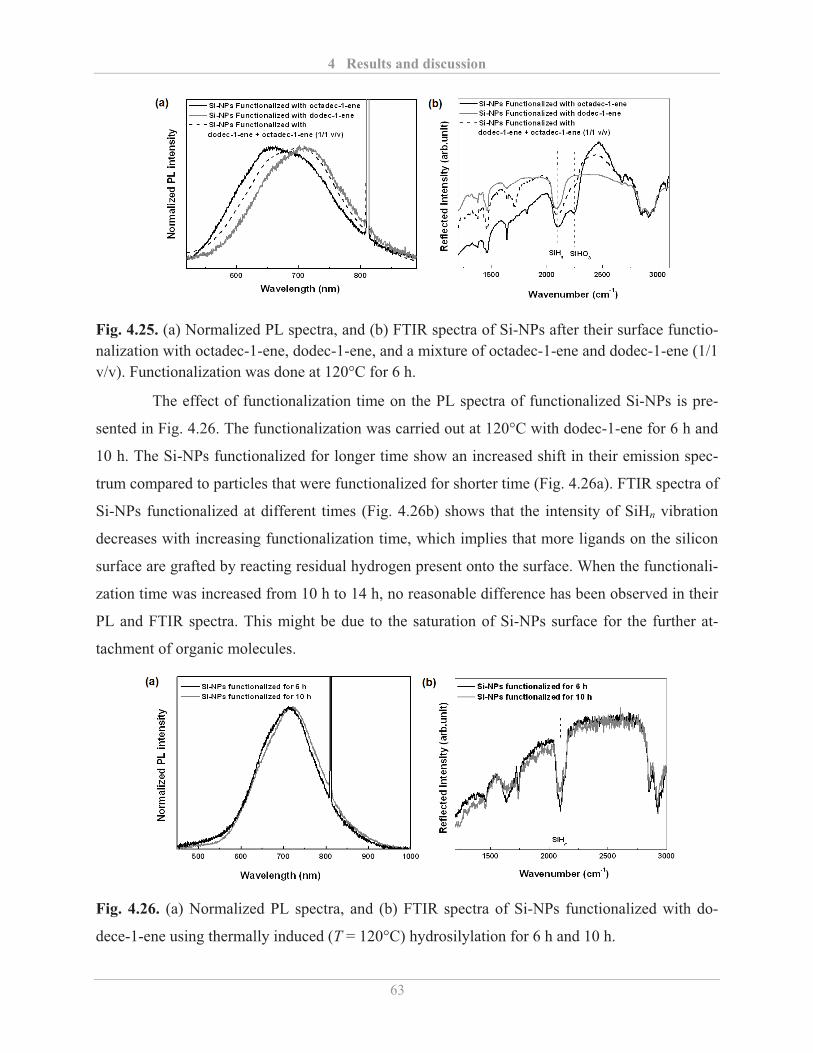
4 Results and discussion
63
Fig. 4.25. (a) Normalized PL spectra, and (b) FTIR spectra of Si-NPs after their surface functio-nalization with octadec-1-ene, dodec-1-ene, and a mixture of octadec-1-ene and dodec-1-ene (1/1 v/v). Functionalization was done at 120°C for 6 h.
The effect of functionalization time on the PL spectra of functionalized Si-NPs is pre-
sented in Fig. 4.26. The functionalization was carried out at 120°C with dodec-1-ene for 6 h and
10 h. The Si-NPs functionalized for longer time show an increased shift in their emission spec-
trum compared to particles that were functionalized for shorter time (Fig. 4.26a). FTIR spectra of
Si-NPs functionalized at different times (Fig. 4.26b) shows that the intensity of SiHn vibration
decreases with increasing functionalization time, which implies that more ligands on the silicon
surface are grafted by reacting residual hydrogen present onto the surface. When the functionali-
zation time was increased from 10 h to 14 h, no reasonable difference has been observed in their
PL and FTIR spectra. This might be due to the saturation of Si-NPs surface for the further at-
tachment of organic molecules.
Fig. 4.26. (a) Normalized PL spectra, and (b) FTIR spectra of Si-NPs functionalized with do-
dece-1-ene using thermally induced (T = 120°C) hydrosilylation for 6 h and 10 h.
4 Results and discussion
64
If we assume that Si-H bonds are only consumed in the formation of Si-C bonds during
surface functionalization, we can compare the coverage of Si-NPs with organic ligands by com-
paring the amount (FTIR intensity) of unreacted SiHn bonds with the initial amount (presuming
that there is no significant oxidation that will consume SiHn bonds). As the surface functionaliza-
tion proceeds, the coverage of the Si-NPs surface with organic molecules increases (Fig. 4.26b).
The organic molecules with longer carbon chain provide lower surface coverage compared to
shorter alkenes because of high steric hindrance, and the particles that undergo mixed surface
functionalization showed intermediate surface coverage (Fig. 4.25b). The Si-NPs show enhanced
coverage of organic ligands on their surface at elevated temperature (Fig.4.22b) and high energy
UV irradiation with 254 nm (Fig. 4.23b). Additionally, the thermally induced hydrosilylation
process gives a higher surface coverage compared to the photoinitiated hydrosilylation (Fig.
4.24b). It is found that the functionalization of Si-NPs using thermally induced hydrosilylation
gives the best surface coverage with dodec-1-ene at temperature 120°C and functionalization
time of 10 h.
All the results shown above give us a hint that surface coverage plays a very prominent
role in determining the PL property of functionalized Si-NPs. It is noteworthy that all the par-
ticles with higher surface coverage (reduced intensity of SiHn vibration signal) showed an in-
creased red shift in their emission spectrum compared to those having a lower coverage of li-
gands (higher intensity of SiHn vibration signal). Despite this fact, no systematic correlation be-
tween the magnitude of the red shift and the surface coverage of Si-NPs is observed. As an edu-
cated guess, one can assume that there is a correlation between the increased size of the particle
(core + shell) with higher surface coverage and the red shift. This assumption is supported by the
fact that the wavefunction within the nanoparticles is not limited to the crystalline silicon core
[135]. Additionally, it is observed that the shape of PL was also influenced by the reaction condi-
tions. A further study is necessary to explore the anomalous PL behavior of functionalized Si-
NPs.
4.2.2.3 Air stability of functionalized Si-NPs
In this study, the air stability of Si-NPs was examined after their surface functionalization with
dodec-1-ene and different kind of esters (ethyl undecylenate (ETU), vinyl benzoate (VB) and
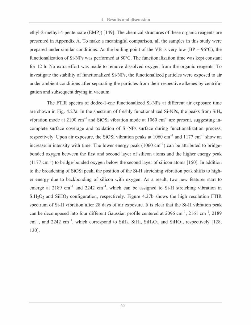
4 Results and discussion
65
ethyl-2-methyl-4-pentenoate (EMP)) [149]. The chemical structures of these organic reagents are
presented in Appendix A. To make a meaningful comparison, all the samples in this study were
prepared under similar conditions. As the boiling point of the VB is very low (BP = 96°C), the
functionalization of Si-NPs was performed at 80°C. The functionalization time was kept constant
for 12 h. No extra effort was made to remove dissolved oxygen from the organic reagents. To
investigate the stability of functionalized Si-NPs, the functionalized particles were exposed to air
under ambient conditions after separating the particles from their respective alkenes by centrifu-
gation and subsequent drying in vacuum.
The FTIR spectra of dodec-1-ene functionalized Si-NPs at different air exposure time
are shown in Fig. 4.27a. In the spectrum of freshly functionalized Si-NPs, the peaks from SiHn
vibration mode at 2100 cm–1 and SiOSi vibration mode at 1060 cm–1 are present, suggesting in-
complete surface coverage and oxidation of Si-NPs surface during functionalization process,
respectively. Upon air exposure, the SiOSi vibration peaks at 1060 cm–1 and 1177 cm–1 show an
increase in intensity with time. The lower energy peak (1060 cm–1) can be attributed to bridge-
bonded oxygen between the first and second layer of silicon atoms and the higher energy peak
(1177 cm–1) to bridge-bonded oxygen below the second layer of silicon atoms [150]. In addition
to the broadening of SiOSi peak, the position of the Si-H stretching vibration peak shifts to high-
er energy due to backbonding of silicon with oxygen. As a result, two new features start to
emerge at 2189 cm–1 and 2242 cm–1, which can be assigned to Si-H stretching vibration in
SiH2O2 and SiHO3 configuration, respectively. Figure 4.27b shows the high resolution FTIR
spectrum of Si-H vibration after 28 days of air exposure. It is clear that the Si-H vibration peak
can be decomposed into four different Gaussian profile centered at 2096 cm–1, 2161 cm–1, 2189
cm–1, and 2242 cm–1, which correspond to SiH2, SiH3, SiH2O2, and SiHO3, respectively [128,
130].
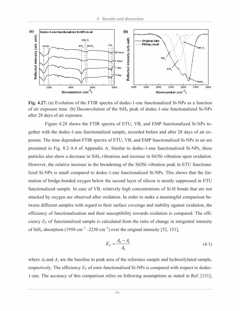
4 Results and discussion
66
Fig. 4.27. (a) Evolution of the FTIR spectra of dodec-1-ene functionalized Si-NPs as a function of air exposure time. (b) Deconvolution of the SiHn peak of dodec-1-ene functionalized Si-NPs after 28 days of air exposure.
Figure 4.28 shows the FTIR spectra of ETU, VB, and EMP functionalized Si-NPs to-
gether with the dodec-1-ene functionalized sample, recorded before and after 28 days of air ex-
posure. The time dependent FTIR spectra of ETU, VB, and EMP functionalized Si-NPs in air are
presented in Fig. 8.2–8.4 of Appendix A. Similar to dodec-1-ene functionalized Si-NPs, these
particles also show a decrease in SiHn vibrations and increase in SiOSi vibration upon oxidation.
However, the relative increase in the broadening of the SiOSi vibration peak in ETU functiona-
lized Si-NPs is small compared to dodec-1-ene functionalized Si-NPs. This shows that the for-
mation of bridge-bonded oxygen below the second layer of silicon is mostly suppressed in ETU
functionalized sample. In case of VB, relatively high concentrations of Si-H bonds that are not
attacked by oxygen are observed after oxidation. In order to make a meaningful comparison be-
tween different samples with regard to their surface coverage and stability against oxidation, the
efficiency of functionalization and their susceptibility towards oxidation is compared. The effi-
ciency EF of functionalized sample is calculated from the ratio of change in integrated intensity
of SiHn absorption (1950 cm–1 –2250 cm–1) over the original intensity [52, 151],
0
10
AAAEF
�� (4.1)
where A0 and A1 are the baseline to peak area of the reference sample and hydrosilylated sample,
respectively. The efficiency EF of ester functionalized Si-NPs is compared with respect to dodec-
1-ene. The accuracy of this comparison relies on following assumptions as stated in Ref. [151];
4 Results and discussion
67
(i) the unit intensities of SiH, SiH2, SiH3 bonds are similar, and (ii) the number of Si-H bonds
that are consumed during the surface functionalization other than in the formation of Si-C bonds
(e.g. in surface oxidation) are same in all the samples.
It is also necessary to define a measure for the relative susceptibility of different func-
tionalized Si-NPs towards air oxidation. As discussed above, during the oxidation process the
intensity of SiOSi vibration signal increases (due to formation of bridge-bonded oxygen) and the
intensity of SiHn vibration decreases (because increased backbonded oxygen shifts its vibration
frequency to higher energies). Therefore, to make a qualitative comparison of the oxidation sus-
ceptibility of different functionalized samples, one can define the oxidation susceptibility index
So as,
days 0SiHSi0Si
28daysSiHSi0Si
)/()/(
n
n
AAAA
So � (4.2)
where ASiOSi and ASiHn are the baseline to peak area of SiOSi absorption (980 cm–1 –1200 cm–1)
and SiHn absorption (1950 cm–1 –2250 cm–1), respectively.
Fig. 4.28. FTIR spectra of dodec-1-ene, VB, EMP and ETU functionalized Si-NPs: Freshly func-tionalized sample (black curves) and after 28 days of surface oxidation in air (gray curves).
Table 4.1 summarizes the relative functionalization efficiency and oxidation susceptibil-
ity index of different functionalized samples. The relative functionalization efficiency of differ-
ent organic reagent is compared with respect to dodec-1-ene. It is found that functionalization of
Si-NPs with dodec-1-ene and ETU gives higher surface coverage compared to VB. Despite of
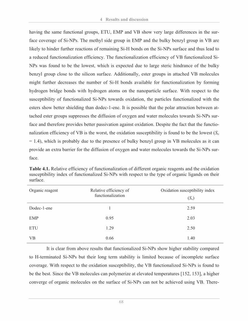
4 Results and discussion
68
having the same functional groups, ETU, EMP and VB show very large differences in the sur-
face coverage of Si-NPs. The methyl side group in EMP and the bulky benzyl group in VB are
likely to hinder further reactions of remaining Si-H bonds on the Si-NPs surface and thus lead to
a reduced functionalization efficiency. The functionalization efficiency of VB functionalized Si-
NPs was found to be the lowest, which is expected due to large steric hindrance of the bulky
benzyl group close to the silicon surface. Additionally, ester groups in attached VB molecules
might further decreases the number of Si-H bonds available for functionalization by forming
hydrogen bridge bonds with hydrogen atoms on the nanoparticle surface. With respect to the
susceptibility of functionalized Si-NPs towards oxidation, the particles functionalized with the
esters show better shielding than dodec-1-ene. It is possible that the polar attraction between at-
tached ester groups suppresses the diffusion of oxygen and water molecules towards Si-NPs sur-
face and therefore provides better passivation against oxidation. Despite the fact that the functio-
nalization efficiency of VB is the worst, the oxidation susceptibility is found to be the lowest (So
= 1.4), which is probably due to the presence of bulky benzyl group in VB molecules as it can
provide an extra barrier for the diffusion of oxygen and water molecules towards the Si-NPs sur-
face.
Table 4.1. Relative efficiency of functionalization of different organic reagents and the oxidation susceptibility index of functionalized Si-NPs with respect to the type of organic ligands on their surface.
Organic reagent Relative efficiency of functionalization
Oxidation susceptibility index
(So)
Dodec-1-ene 1 2.59
EMP 0.95 2.03
ETU 1.29 2.50
VB 0.66 1.40
It is clear from above results that functionalized Si-NPs show higher stability compared
to H-terminated Si-NPs but their long term stability is limited because of incomplete surface
coverage. With respect to the oxidation susceptibility, the VB functionalized Si-NPs is found to
be the best. Since the VB molecules can polymerize at elevated temperatures [152, 153], a higher
converge of organic molecules on the surface of Si-NPs can not be achieved using VB. There-
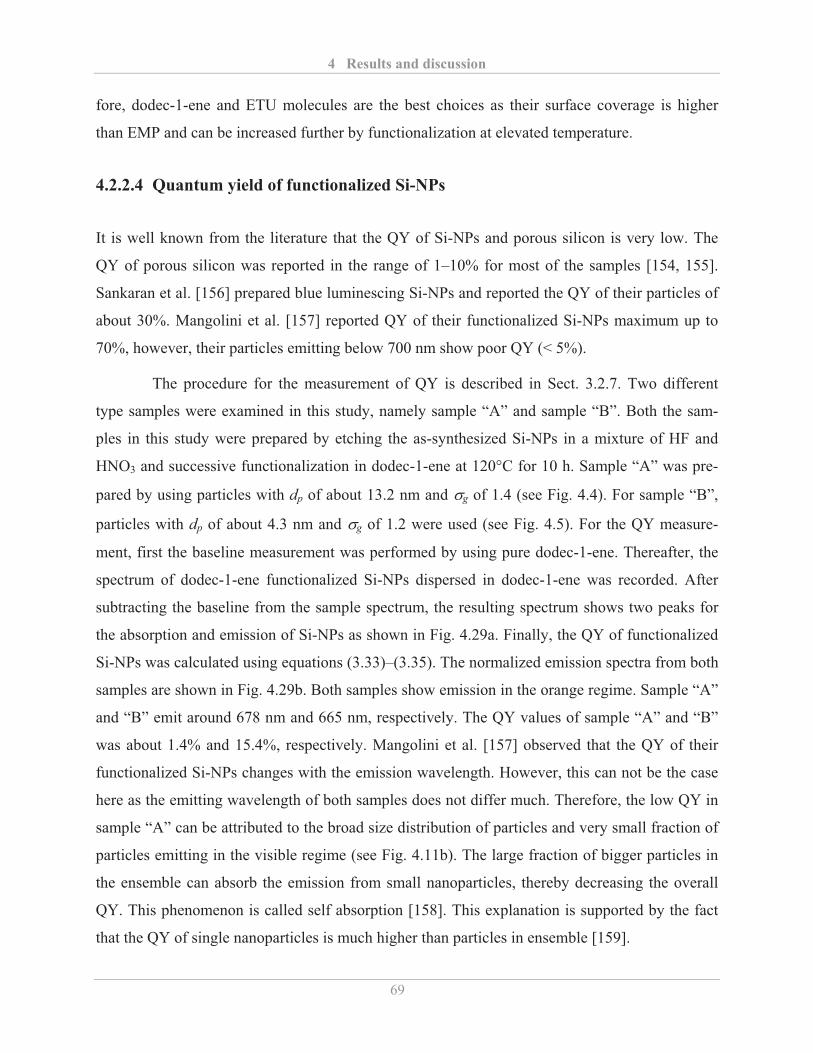
4 Results and discussion
69
fore, dodec-1-ene and ETU molecules are the best choices as their surface coverage is higher
than EMP and can be increased further by functionalization at elevated temperature.
4.2.2.4 Quantum yield of functionalized Si-NPs
It is well known from the literature that the QY of Si-NPs and porous silicon is very low. The
QY of porous silicon was reported in the range of 1–10% for most of the samples [154, 155].
Sankaran et al. [156] prepared blue luminescing Si-NPs and reported the QY of their particles of
about 30%. Mangolini et al. [157] reported QY of their functionalized Si-NPs maximum up to
70%, however, their particles emitting below 700 nm show poor QY (< 5%).
The procedure for the measurement of QY is described in Sect. 3.2.7. Two different
type samples were examined in this study, namely sample “A” and sample “B”. Both the sam-
ples in this study were prepared by etching the as-synthesized Si-NPs in a mixture of HF and
HNO3 and successive functionalization in dodec-1-ene at 120°C for 10 h. Sample “A” was pre-
pared by using particles with dp of about 13.2 nm and �g of 1.4 (see Fig. 4.4). For sample “B”,
particles with dp of about 4.3 nm and �g of 1.2 were used (see Fig. 4.5). For the QY measure-
ment, first the baseline measurement was performed by using pure dodec-1-ene. Thereafter, the
spectrum of dodec-1-ene functionalized Si-NPs dispersed in dodec-1-ene was recorded. After
subtracting the baseline from the sample spectrum, the resulting spectrum shows two peaks for
the absorption and emission of Si-NPs as shown in Fig. 4.29a. Finally, the QY of functionalized
Si-NPs was calculated using equations (3.33)–(3.35). The normalized emission spectra from both
samples are shown in Fig. 4.29b. Both samples show emission in the orange regime. Sample “A”
and “B” emit around 678 nm and 665 nm, respectively. The QY values of sample “A” and “B”
was about 1.4% and 15.4%, respectively. Mangolini et al. [157] observed that the QY of their
functionalized Si-NPs changes with the emission wavelength. However, this can not be the case
here as the emitting wavelength of both samples does not differ much. Therefore, the low QY in
sample “A” can be attributed to the broad size distribution of particles and very small fraction of
particles emitting in the visible regime (see Fig. 4.11b). The large fraction of bigger particles in
the ensemble can absorb the emission from small nanoparticles, thereby decreasing the overall
QY. This phenomenon is called self absorption [158]. This explanation is supported by the fact
that the QY of single nanoparticles is much higher than particles in ensemble [159].
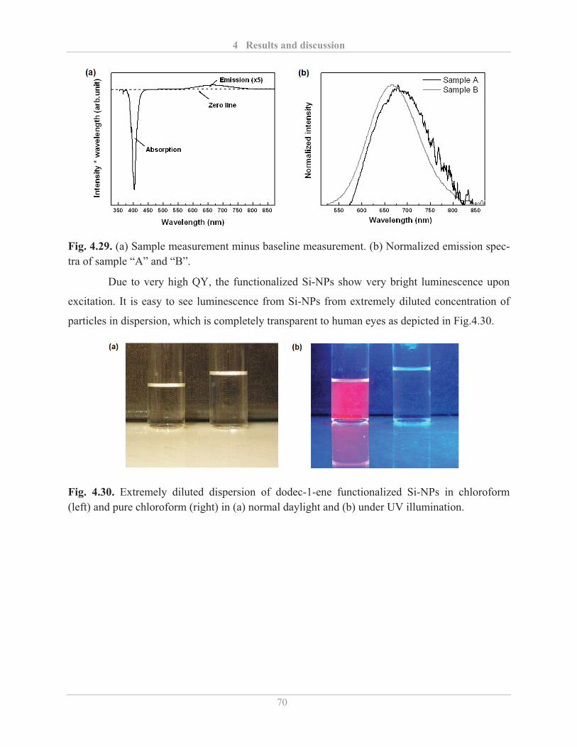
4 Results and discussion
70
Fig. 4.29. (a) Sample measurement minus baseline measurement. (b) Normalized emission spec-tra of sample “A” and “B”.
Due to very high QY, the functionalized Si-NPs show very bright luminescence upon
excitation. It is easy to see luminescence from Si-NPs from extremely diluted concentration of
particles in dispersion, which is completely transparent to human eyes as depicted in Fig.4.30.
Fig. 4.30. Extremely diluted dispersion of dodec-1-ene functionalized Si-NPs in chloroform (left) and pure chloroform (right) in (a) normal daylight and (b) under UV illumination.
4 Results and discussion
71
4.3 Electrical properties of Si-NPs
In our group, the size dependent electrical conductivity of as-synthesized Si-NPs has already
been studied. It was observed that the electrical conductivity of as-synthesized Si-NPs decreases
with decreasing size [160]. In this study, the influence of surface modification on the electrical
conductivity of Si-NPs was examined. Due to the fact that small Si-NPs show very poor electric-
al conductivity, Si-NPs with a mean diameter of about 52 nm (see Fig. 4.2) were examined in
this study. Thin pellets of Si-NPs were prepared by pressing the powder uniaxially and the elec-
trical conductivity of pressed pellet was measured using impedance spectrometry (see Sect. 3.2.3
for details). The measurements were done under hydrogen atmosphere in order to avoid the oxi-
dation of Si-NPs during the experiments.
The typical Nyquist diagram of the impedance measurements of Si-NPs in the tempera-
ture range between 100°C and 400°C is shown in Fig. 4.31. It is clear that the resistance of Si-
NPs decreases with increasing temperature. All the samples under this study show similar beha-
vior. The intercept of the semicircle at low frequency gives the total resistance (Rt), which can be
converted into specific conductivity (�) by,
ct
p
ART
�� (4.4)
where Tp is the thickness and Ac is the cross section area of the pellet.
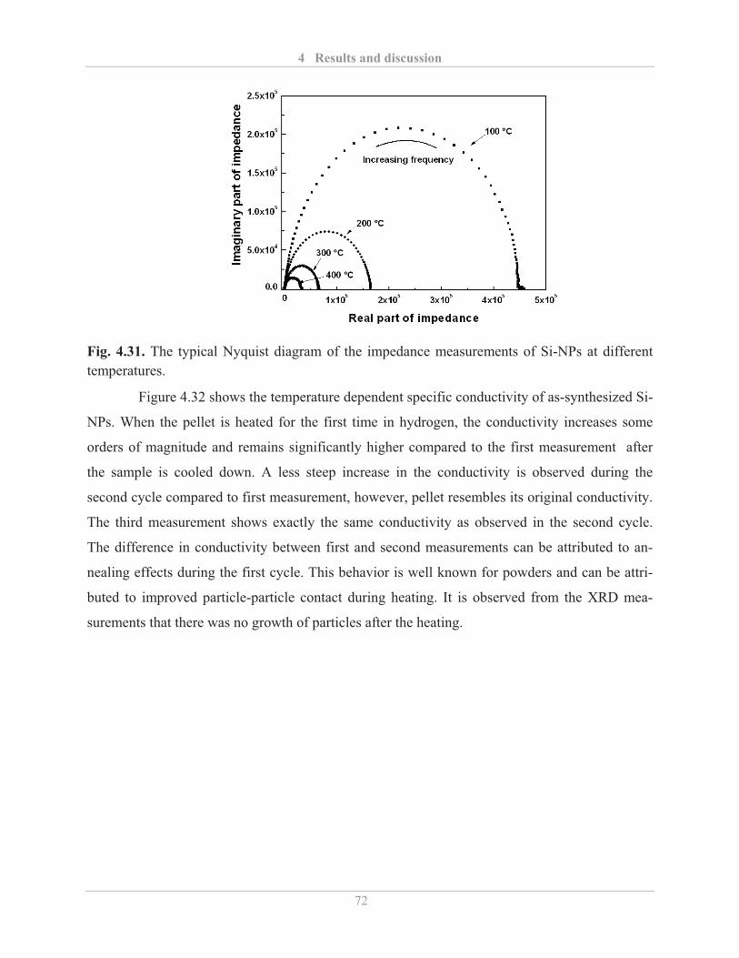
4 Results and discussion
72
Fig. 4.31. The typical Nyquist diagram of the impedance measurements of Si-NPs at different temperatures.
Figure 4.32 shows the temperature dependent specific conductivity of as-synthesized Si-
NPs. When the pellet is heated for the first time in hydrogen, the conductivity increases some
orders of magnitude and remains significantly higher compared to the first measurement after
the sample is cooled down. A less steep increase in the conductivity is observed during the
second cycle compared to first measurement, however, pellet resembles its original conductivity.
The third measurement shows exactly the same conductivity as observed in the second cycle.
The difference in conductivity between first and second measurements can be attributed to an-
nealing effects during the first cycle. This behavior is well known for powders and can be attri-
buted to improved particle-particle contact during heating. It is observed from the XRD mea-
surements that there was no growth of particles after the heating.
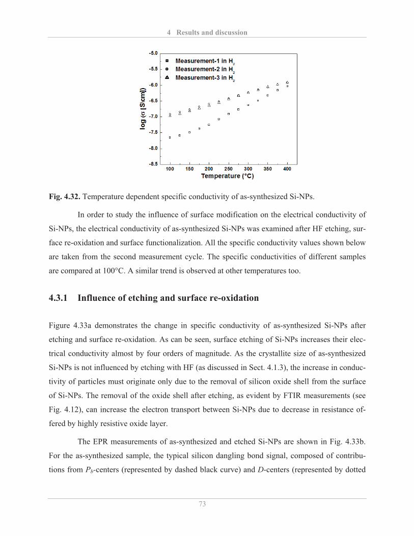
4 Results and discussion
73
Fig. 4.32. Temperature dependent specific conductivity of as-synthesized Si-NPs.
In order to study the influence of surface modification on the electrical conductivity of
Si-NPs, the electrical conductivity of as-synthesized Si-NPs was examined after HF etching, sur-
face re-oxidation and surface functionalization. All the specific conductivity values shown below
are taken from the second measurement cycle. The specific conductivities of different samples
are compared at 100°C. A similar trend is observed at other temperatures too.
4.3.1 Influence of etching and surface re-oxidation
Figure 4.33a demonstrates the change in specific conductivity of as-synthesized Si-NPs after
etching and surface re-oxidation. As can be seen, surface etching of Si-NPs increases their elec-
trical conductivity almost by four orders of magnitude. As the crystallite size of as-synthesized
Si-NPs is not influenced by etching with HF (as discussed in Sect. 4.1.3), the increase in conduc-
tivity of particles must originate only due to the removal of silicon oxide shell from the surface
of Si-NPs. The removal of the oxide shell after etching, as evident by FTIR measurements (see
Fig. 4.12), can increase the electron transport between Si-NPs due to decrease in resistance of-
fered by highly resistive oxide layer.
The EPR measurements of as-synthesized and etched Si-NPs are shown in Fig. 4.33b.
For the as-synthesized sample, the typical silicon dangling bond signal, composed of contribu-
tions from Pb-centers (represented by dashed black curve) and D-centers (represented by dotted
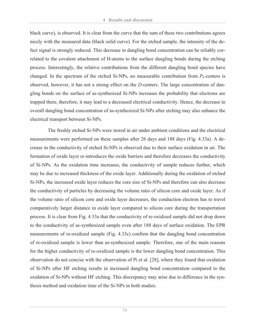
4 Results and discussion
74
black curve), is observed. It is clear from the curve that the sum of these two contributions agrees
nicely with the measured data (black solid curve). For the etched sample, the intensity of the de-
fect signal is strongly reduced. This decrease in dangling bond concentration can be reliably cor-
related to the covalent attachment of H-atoms to the surface dangling bonds during the etching
process. Interestingly, the relative contributions from the different dangling bond species have
changed. In the spectrum of the etched Si-NPs, no measurable contribution from Pb-centers is
observed, however, it has not a strong effect on the D-centers. The large concentration of dan-
gling bonds on the surface of as-synthesized Si-NPs increases the probability that electrons are
trapped there, therefore, it may lead to a decreased electrical conductivity. Hence, the decrease in
overall dangling bond concentration of as-synthesized Si-NPs after etching may also enhance the
electrical transport between Si-NPs.
The freshly etched Si-NPs were stored in air under ambient conditions and the electrical
measurements were performed on these samples after 26 days and 188 days (Fig. 4.33a). A de-
crease in the conductivity of etched Si-NPs is observed due to their surface oxidation in air. The
formation of oxide layer re-introduces the oxide barriers and therefore decreases the conductivity
of Si-NPs. As the oxidation time increases, the conductivity of sample reduces further, which
may be due to increased thickness of the oxide layer. Additionally during the oxidation of etched
Si-NPs, the increased oxide layer reduces the core size of Si-NPs and therefore can also decrease
the conductivity of particles by decreasing the volume ratio of silicon core and oxide layer. As if
the volume ratio of silicon core and oxide layer decreases, the conduction electron has to travel
comparatively larger distance in oxide layer compared to silicon core during the transportation
process. It is clear from Fig. 4.33a that the conductivity of re-oxidized sample did not drop down
to the conductivity of as-synthesized sample even after 188 days of surface oxidation. The EPR
measurements of re-oxidized sample (Fig. 4.33c) confirm that the dangling bond concentration
of re-oxidized sample is lower than as-synthesized sample. Therefore, one of the main reasons
for the higher conductivity of re-oxidized sample is the lower dangling bond concentration. This
observation do not concise with the observation of Pi et al. [28], where they found that oxidation
of Si-NPs after HF etching results in increased dangling bond concentration compared to the
oxidation of Si-NPs without HF etching. This discrepancy may arise due to difference in the syn-
thesis method and oxidation time of the Si-NPs in both studies.
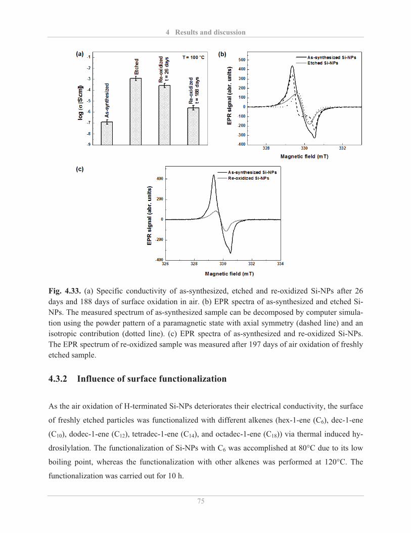
4 Results and discussion
75
Fig. 4.33. (a) Specific conductivity of as-synthesized, etched and re-oxidized Si-NPs after 26 days and 188 days of surface oxidation in air. (b) EPR spectra of as-synthesized and etched Si-NPs. The measured spectrum of as-synthesized sample can be decomposed by computer simula-tion using the powder pattern of a paramagnetic state with axial symmetry (dashed line) and an isotropic contribution (dotted line). (c) EPR spectra of as-synthesized and re-oxidized Si-NPs. The EPR spectrum of re-oxidized sample was measured after 197 days of air oxidation of freshly etched sample.
4.3.2 Influence of surface functionalization
As the air oxidation of H-terminated Si-NPs deteriorates their electrical conductivity, the surface
of freshly etched particles was functionalized with different alkenes (hex-1-ene (C6), dec-1-ene
(C10), dodec-1-ene (C12), tetradec-1-ene (C14), and octadec-1-ene (C18)) via thermal induced hy-
drosilylation. The functionalization of Si-NPs with C6 was accomplished at 80°C due to its low
boiling point, whereas the functionalization with other alkenes was performed at 120°C. The
functionalization was carried out for 10 h.
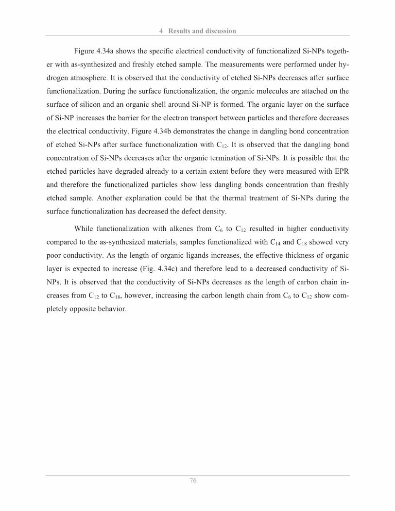
4 Results and discussion
76
Figure 4.34a shows the specific electrical conductivity of functionalized Si-NPs togeth-
er with as-synthesized and freshly etched sample. The measurements were performed under hy-
drogen atmosphere. It is observed that the conductivity of etched Si-NPs decreases after surface
functionalization. During the surface functionalization, the organic molecules are attached on the
surface of silicon and an organic shell around Si-NP is formed. The organic layer on the surface
of Si-NP increases the barrier for the electron transport between particles and therefore decreases
the electrical conductivity. Figure 4.34b demonstrates the change in dangling bond concentration
of etched Si-NPs after surface functionalization with C12. It is observed that the dangling bond
concentration of Si-NPs decreases after the organic termination of Si-NPs. It is possible that the
etched particles have degraded already to a certain extent before they were measured with EPR
and therefore the functionalized particles show less dangling bonds concentration than freshly
etched sample. Another explanation could be that the thermal treatment of Si-NPs during the
surface functionalization has decreased the defect density.
While functionalization with alkenes from C6 to C12 resulted in higher conductivity
compared to the as-synthesized materials, samples functionalized with C14 and C18 showed very
poor conductivity. As the length of organic ligands increases, the effective thickness of organic
layer is expected to increase (Fig. 4.34c) and therefore lead to a decreased conductivity of Si-
NPs. It is observed that the conductivity of Si-NPs decreases as the length of carbon chain in-
creases from C12 to C18, however, increasing the carbon length chain from C6 to C12 show com-
pletely opposite behavior.
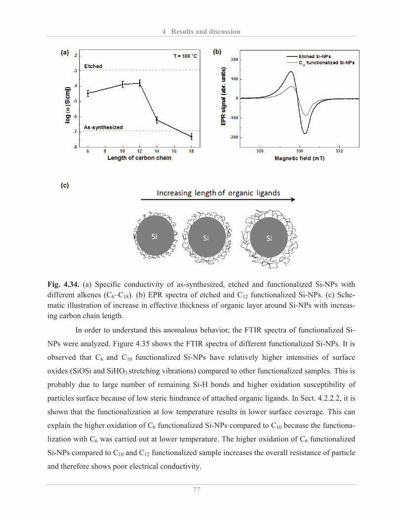
4 Results and discussion
77
Fig. 4.34. (a) Specific conductivity of as-synthesized, etched and functionalized Si-NPs with different alkenes (C6–C18). (b) EPR spectra of etched and C12 functionalized Si-NPs. (c) Sche-matic illustration of increase in effective thickness of organic layer around Si-NPs with increas-ing carbon chain length.
In order to understand this anomalous behavior, the FTIR spectra of functionalized Si-
NPs were analyzed. Figure 4.35 shows the FTIR spectra of different functionalized Si-NPs. It is
observed that C6 and C10 functionalized Si-NPs have relatively higher intensities of surface
oxides (SiOSi and SiHO3 stretching vibrations) compared to other functionalized samples. This is
probably due to large number of remaining Si-H bonds and higher oxidation susceptibility of
particles surface because of low steric hindrance of attached organic ligands. In Sect. 4.2.2.2, it is
shown that the functionalization at low temperature results in lower surface coverage. This can
explain the higher oxidation of C6 functionalized Si-NPs compared to C10 because the functiona-
lization with C6 was carried out at lower temperature. The higher oxidation of C6 functionalized
Si-NPs compared to C10 and C12 functionalized sample increases the overall resistance of particle
and therefore shows poor electrical conductivity.
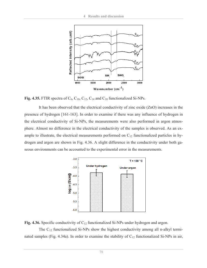
4 Results and discussion
78
Fig. 4.35. FTIR spectra of C6, C10, C12, C14 and C18 functionalized Si-NPs.
It has been observed that the electrical conductivity of zinc oxide (ZnO) increases in the
presence of hydrogen [161-163]. In order to examine if there was any influence of hydrogen in
the electrical conductivity of Si-NPs, the measurements were also performed in argon atmos-
phere. Almost no difference in the electrical conductivity of the samples is observed. As an ex-
ample to illustrate, the electrical measurements performed on C12 functionalized particles in hy-
drogen and argon are shown in Fig. 4.36. A slight difference in the conductivity under both ga-
seous environments can be accounted to the experimental error in the measurements.
Fig. 4.36. Specific conductivity of C12 functionalized Si-NPs under hydrogen and argon.
The C12 functionalized Si-NPs show the highest conductivity among all n-alkyl termi-
nated samples (Fig. 4.34a). In order to examine the stability of C12 functionalized Si-NPs in air,
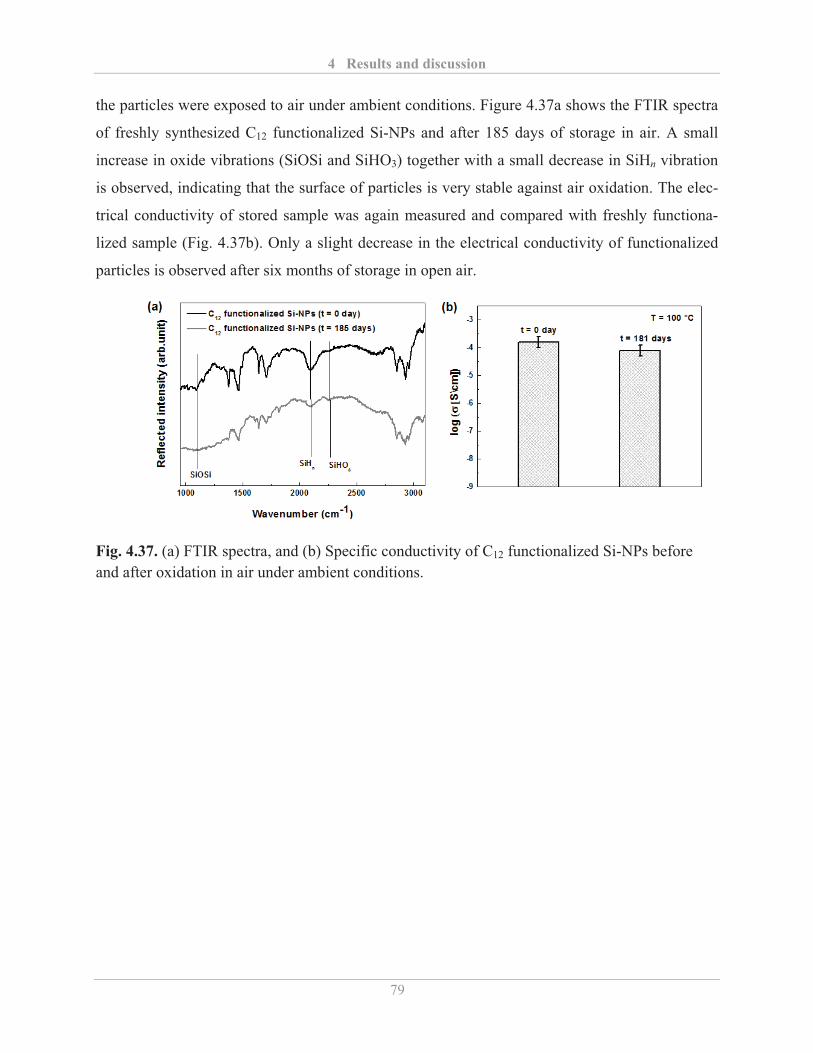
4 Results and discussion
79
the particles were exposed to air under ambient conditions. Figure 4.37a shows the FTIR spectra
of freshly synthesized C12 functionalized Si-NPs and after 185 days of storage in air. A small
increase in oxide vibrations (SiOSi and SiHO3) together with a small decrease in SiHn vibration
is observed, indicating that the surface of particles is very stable against air oxidation. The elec-
trical conductivity of stored sample was again measured and compared with freshly functiona-
lized sample (Fig. 4.37b). Only a slight decrease in the electrical conductivity of functionalized
particles is observed after six months of storage in open air.
Fig. 4.37. (a) FTIR spectra, and (b) Specific conductivity of C12 functionalized Si-NPs before and after oxidation in air under ambient conditions.
4 Results and discussion
80
4.4 Dispersion stability and ink-jet printing of Si-NPs
In this section, the stability of as-synthesized, etched and functionalized Si-NPs dispersion is
examined. Additionally, it is shown that the functionalized Si-NPs can be used to print structures
on a substrate.
4.4.1 Stability of Si-NPs dispersion
The particles with mean diameter of about 4.3 nm were examined in this study (see Fig. 4.5).
The freshly etched Si-NPs are prepared by etching the as-synthesized Si-NPs in HF. It is shown
earlier in Sect. 4.2.2.3 that ETU functionalized Si-NPs show the highest surface coverage com-
pared to other alkenes under this study. Therefore, the surface functionalization of Si-NPs was
carried out with ETU at 120°C for 10 h.
Figure 4.38a,b shows a schematic representation of as-synthesized, freshly etched and
functionalized Si-NPs dispersion together with their dispersion stability in air under ambient
conditions. It is observed that as-synthesized Si-NPs are very difficult to disperse because the
particles are highly agglomerated (Fig. 4.38c). Additionally, the presence of oxide shell around
the Si-NPs also limits the choice of dispersion medium for as-synthesized particles. It is seen that
as-synthesized Si-NPs can be dispersed in de-ionized water but not without ultrasonic agitation.
The dispersion of as-synthesized Si-NPs in de-ionized water is shown in Fig. 4.38b (vial “A”).
The dispersion is visibly turbid due to presence of agglomerates. The average diameter of ag-
glomerated as-synthesized Si-NPs measured using dynamic light scattering was about 117 nm
(see Fig. 8.6a of Appendix A), which is about 28 times larger than their mean particle diameter.
It is found that the zeta potential of the dispersion is not very high (< 40 mV, Fig. 8.6b of Ap-
pendix A), as a result a significant sedimentation of particles is observed after 2 hours. The etch-
ing of Si-NPs with HF removes the oxide layer and breaks the agglomeration of Si-NPs (see Fig.
4.12, Sect. 4.1.3). However, it is found that the etched Si-NPs also do not form a stable disper-
sion in solvents because of the re-oxidation of particle. Also, etched Si-NPs are aggregated due
to formation of oxide layer around them (see Sect 4.1.1). As an example to demonstrate, the dis-
persion stability of etched Si-NPs in chloroform is shown in Fig. 4.38b (vial “B”). A significant
4 Results and discussion
81
agglomeration of particle can be seen after 1 days of storage. The functionalization of freshly
etched Si-NPs with organic molecules using hydrosilylation process provides passivation against
surface re-oxidation. Additionally, the organic layer on the surface of Si-NPs provides steric hin-
drance for the further agglomeration of particles. The functionalized Si-NPs can be dispersed in
organic solvent without any sonication due to presence of organic layer on their surface. In Fig.
4.38b (vial “C”), the dispersion of functionalized Si-NPs in ETU solvent is shown. However, it is
seen that after separating the functionalized Si-NPs from their respective alkenes, the particles
can be re-dispersed in a variety of organic solvents (such as chloroform, toluene, n-hexane etc.)
and the dispersion is extremely stable. The functionalized Si-NPs form a clear dispersion due to
presence of non-agglomerated particles (Fig. 4.38c). The preservation of a non-polar particle
surface provides better dispersability and long-term stability in organic solvents. The average
diameter of functionalized Si-NPs measured using dynamic light scattering was about 28 nm,
which is bigger than the mean particle diameter of as-synthesized Si-NPs due to the coating with
organic molecules and probably some remaining agglomeration. No reasonable change in hydro-
dynamic diameter of functionalized Si-NPs is observed after 1 week of storage (see Fig. 8.7 of
Appendix A), indicating that the dispersion is stable with time and no sedimentation of functio-
nalized Si-NPs was observed even after eight months (visible inspection). The functionalized Si-
NPs can also be dispersed in aqueous solvents by using hydrophilic ligands [164].
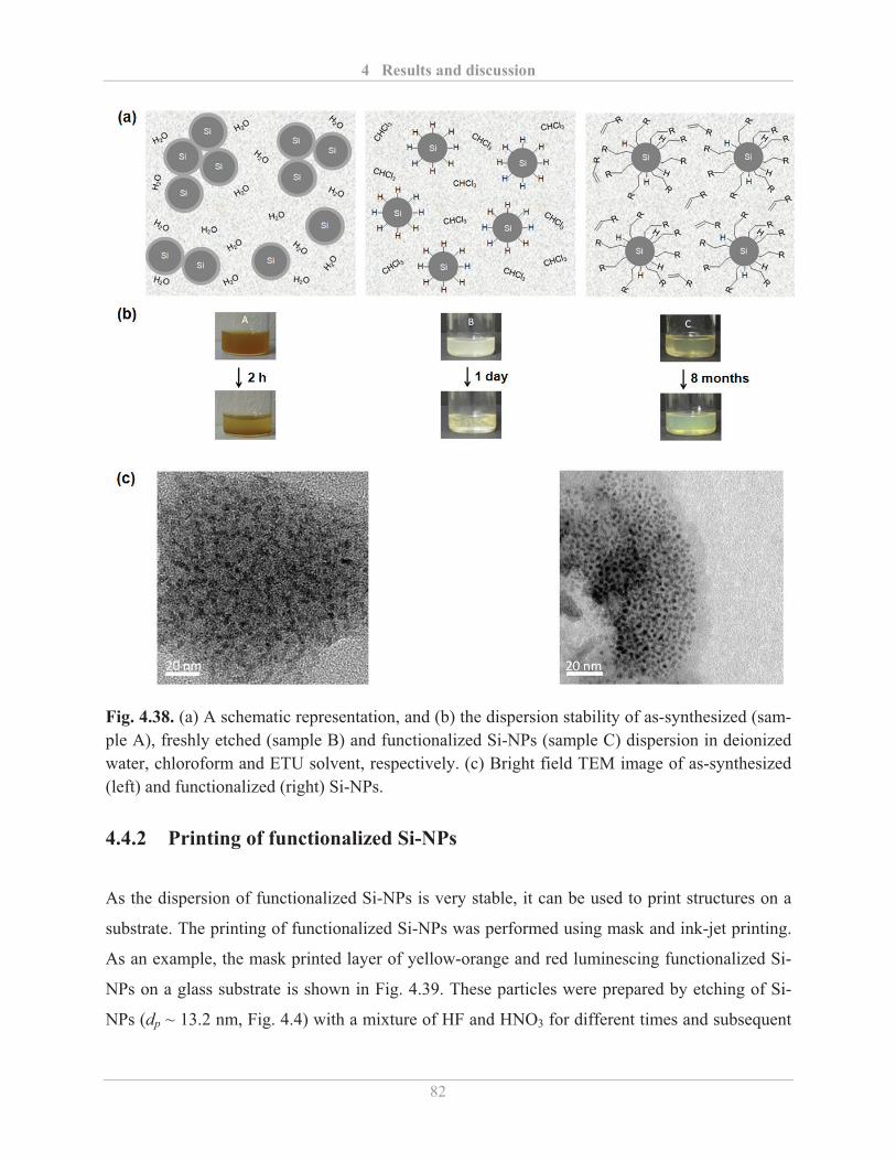
4 Results and discussion
82
Fig. 4.38. (a) A schematic representation, and (b) the dispersion stability of as-synthesized (sam-ple A), freshly etched (sample B) and functionalized Si-NPs (sample C) dispersion in deionized water, chloroform and ETU solvent, respectively. (c) Bright field TEM image of as-synthesized (left) and functionalized (right) Si-NPs.
4.4.2 Printing of functionalized Si-NPs
As the dispersion of functionalized Si-NPs is very stable, it can be used to print structures on a
substrate. The printing of functionalized Si-NPs was performed using mask and ink-jet printing.
As an example, the mask printed layer of yellow-orange and red luminescing functionalized Si-
NPs on a glass substrate is shown in Fig. 4.39. These particles were prepared by etching of Si-
NPs (dp ~ 13.2 nm, Fig. 4.4) with a mixture of HF and HNO3 for different times and subsequent
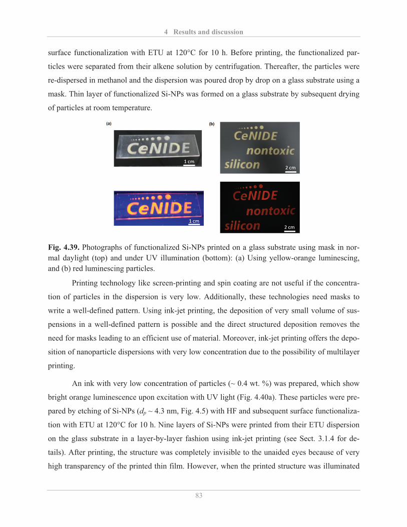
4 Results and discussion
83
surface functionalization with ETU at 120°C for 10 h. Before printing, the functionalized par-
ticles were separated from their alkene solution by centrifugation. Thereafter, the particles were
re-dispersed in methanol and the dispersion was poured drop by drop on a glass substrate using a
mask. Thin layer of functionalized Si-NPs was formed on a glass substrate by subsequent drying
of particles at room temperature.
Fig. 4.39. Photographs of functionalized Si-NPs printed on a glass substrate using mask in nor-mal daylight (top) and under UV illumination (bottom): (a) Using yellow-orange luminescing, and (b) red luminescing particles.
Printing technology like screen-printing and spin coating are not useful if the concentra-
tion of particles in the dispersion is very low. Additionally, these technologies need masks to
write a well-defined pattern. Using ink-jet printing, the deposition of very small volume of sus-
pensions in a well-defined pattern is possible and the direct structured deposition removes the
need for masks leading to an efficient use of material. Moreover, ink-jet printing offers the depo-
sition of nanoparticle dispersions with very low concentration due to the possibility of multilayer
printing.
An ink with very low concentration of particles (~ 0.4 wt. %) was prepared, which show
bright orange luminescence upon excitation with UV light (Fig. 4.40a). These particles were pre-
pared by etching of Si-NPs (dp ~ 4.3 nm, Fig. 4.5) with HF and subsequent surface functionaliza-
tion with ETU at 120°C for 10 h. Nine layers of Si-NPs were printed from their ETU dispersion
on the glass substrate in a layer-by-layer fashion using ink-jet printing (see Sect. 3.1.4 for de-
tails). After printing, the structure was completely invisible to the unaided eyes because of very
high transparency of the printed thin film. However, when the printed structure was illuminated
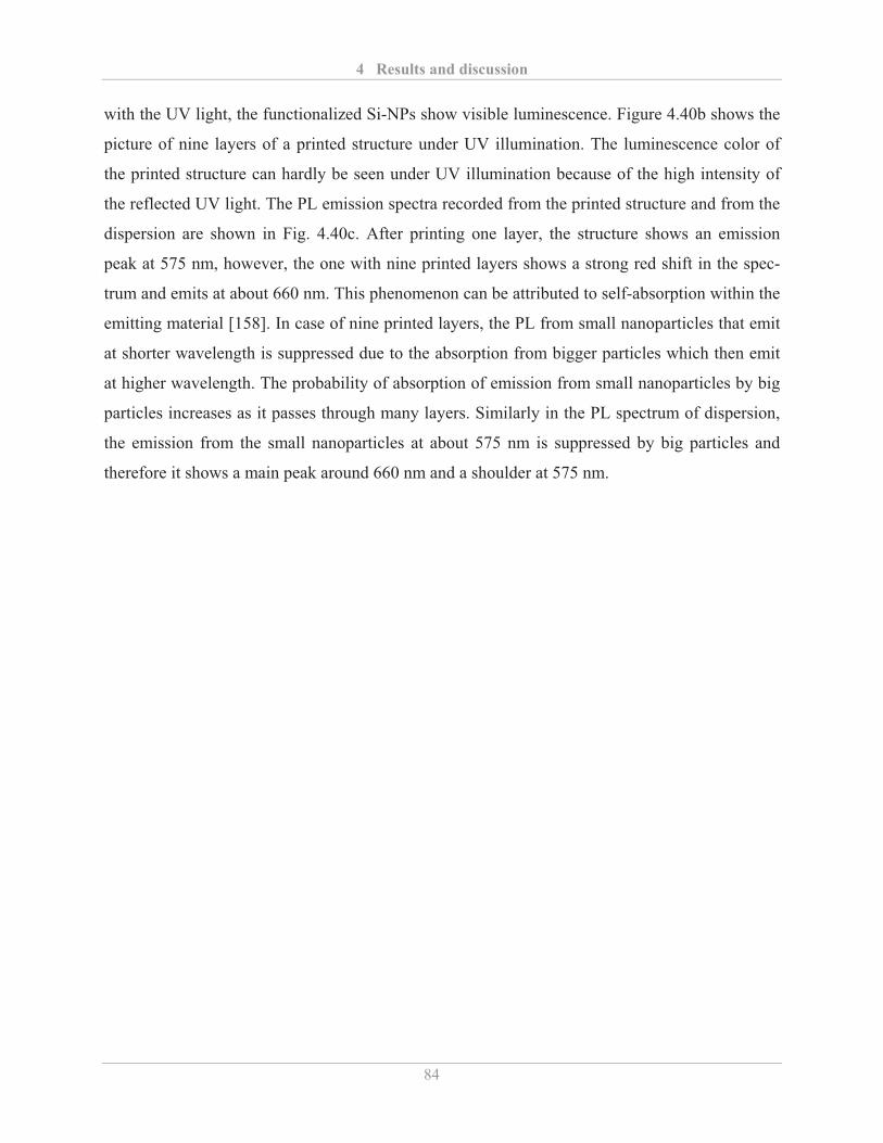
4 Results and discussion
84
with the UV light, the functionalized Si-NPs show visible luminescence. Figure 4.40b shows the
picture of nine layers of a printed structure under UV illumination. The luminescence color of
the printed structure can hardly be seen under UV illumination because of the high intensity of
the reflected UV light. The PL emission spectra recorded from the printed structure and from the
dispersion are shown in Fig. 4.40c. After printing one layer, the structure shows an emission
peak at 575 nm, however, the one with nine printed layers shows a strong red shift in the spec-
trum and emits at about 660 nm. This phenomenon can be attributed to self-absorption within the
emitting material [158]. In case of nine printed layers, the PL from small nanoparticles that emit
at shorter wavelength is suppressed due to the absorption from bigger particles which then emit
at higher wavelength. The probability of absorption of emission from small nanoparticles by big
particles increases as it passes through many layers. Similarly in the PL spectrum of dispersion,
the emission from the small nanoparticles at about 575 nm is suppressed by big particles and
therefore it shows a main peak around 660 nm and a shoulder at 575 nm.
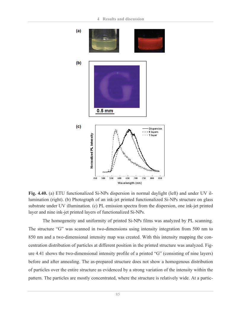
4 Results and discussion
85
Fig. 4.40. (a) ETU functionalized Si-NPs dispersion in normal daylight (left) and under UV il-lumination (right). (b) Photograph of an ink-jet printed functionalized Si-NPs structure on glass substrate under UV illumination. (c) PL emission spectra from the dispersion, one ink-jet printed layer and nine ink-jet printed layers of functionalized Si-NPs.
The homogeneity and uniformity of printed Si-NPs films was analyzed by PL scanning.
The structure “G” was scanned in two-dimensions using intensity integration from 500 nm to
850 nm and a two-dimensional intensity map was created. With this intensity mapping the con-
centration distribution of particles at different position in the printed structure was analyzed. Fig-
ure 4.41 shows the two-dimensional intensity profile of a printed “G” (consisting of nine layers)
before and after annealing. The as-prepared structure does not show a homogenous distribution
of particles over the entire structure as evidenced by a strong variation of the intensity within the
pattern. The particles are mostly concentrated, where the structure is relatively wide. At a partic-
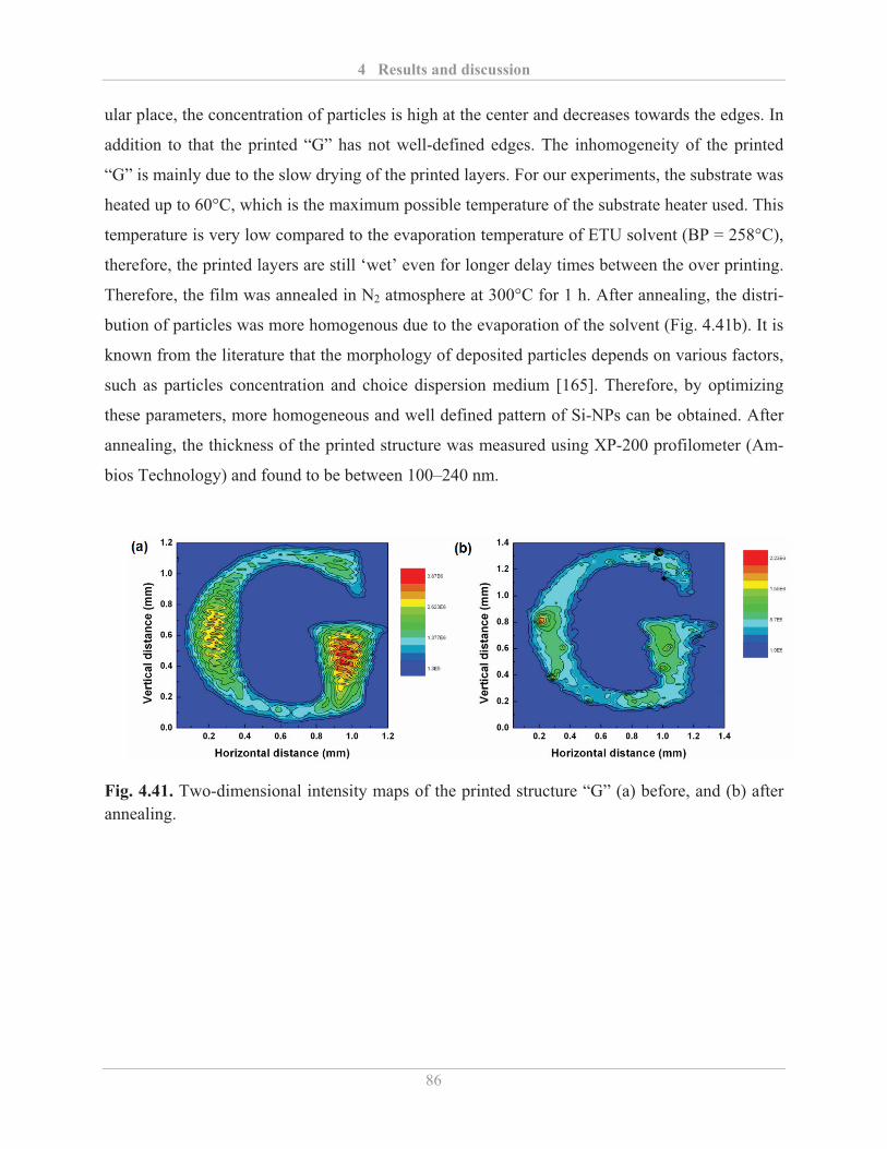
4 Results and discussion
86
ular place, the concentration of particles is high at the center and decreases towards the edges. In
addition to that the printed “G” has not well-defined edges. The inhomogeneity of the printed
“G” is mainly due to the slow drying of the printed layers. For our experiments, the substrate was
heated up to 60°C, which is the maximum possible temperature of the substrate heater used. This
temperature is very low compared to the evaporation temperature of ETU solvent (BP = 258°C),
therefore, the printed layers are still ‘wet’ even for longer delay times between the over printing.
Therefore, the film was annealed in N2 atmosphere at 300°C for 1 h. After annealing, the distri-
bution of particles was more homogenous due to the evaporation of the solvent (Fig. 4.41b). It is
known from the literature that the morphology of deposited particles depends on various factors,
such as particles concentration and choice dispersion medium [165]. Therefore, by optimizing
these parameters, more homogeneous and well defined pattern of Si-NPs can be obtained. After
annealing, the thickness of the printed structure was measured using XP-200 profilometer (Am-
bios Technology) and found to be between 100–240 nm.
Fig. 4.41. Two-dimensional intensity maps of the printed structure “G” (a) before, and (b) after annealing.
4 Results and discussion
87
4.5 Synthesis of cross-linked Si-NPs network
The particles are arranged in two- or three-dimensions after the printing, which can also be
achieved by cross-linking of nanoparticles. The printing creates an artificial arrangement of par-
ticles, whereas the cross-linking of nanoparticles allows them to form interconnected particles.
The cross-linked nanoparticles exhibit new properties, which are quite different from individual
particles. It has been observed that the size of nanoparticles and the inter-particle spacing play a
crucial role in controlling the properties of networked nanoparticles. For example, Storhoff et al.
[63] observed that the optical property of cross-linked Au nanoparticles through DNA depends
on the DNA linker length. Brust et al. [62], studied the electrical properties of Au nanoparticles
cross-linked with dithiol. They observed a strong dependence of the electrical properties on the
size of nanoparticles and the length of the spacer layer. Simon et al. [61] observed that the acti-
vation energy, which is needed for the hopping of the electron from one particle to another par-
ticle during the transportation process, increases after inserting the spacer molecule between
Pd561phen36O200 nanoparticles.
In this section, an approach to form Si-NPs network by the cross-linking of particles
with organic spacer molecules is presented. The key idea is to use the bifunctional organic mole-
cules, which can bind Si-NPs from both sides. Since alkyl terminated Si-NPs are obtained by
hydrosilylation of H-terminated Si-NPs with alkene, the cross-linking of particles can be
achieved via surface functionalization with bidental alkenes (such as 1,7-octadiene).
Figure 4.42 shows the simplified sketch of the formation of silicon-organic networks by
the cross-linking of Si-NPs with bifunctional spacer molecules (1,7-octadiene). The presence of
C=C bond at both end of 1,7-octadiene molecules allow them to bond with two Si-NPs and
therefore this reaction leads to the formation of a three-dimensional network of particles inter-
connection through organic molecules (Fig. 4.42b). It should be noted that not all 1,7-octadiene
molecules, after the attachment of Si-NPs from one side, can bind Si-NPs from another side due
to large steric hindrance. It is also possible that C=C bond at both ends of 1,7-octadiene molecule
are bonded to the same nanoparticle.
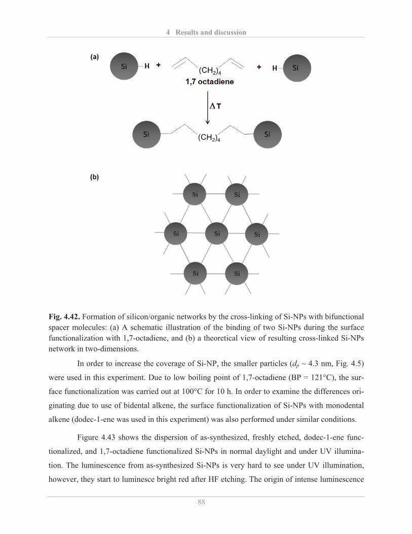
4 Results and discussion
88
Fig. 4.42. Formation of silicon/organic networks by the cross-linking of Si-NPs with bifunctional spacer molecules: (a) A schematic illustration of the binding of two Si-NPs during the surface functionalization with 1,7-octadiene, and (b) a theoretical view of resulting cross-linked Si-NPs network in two-dimensions.
In order to increase the coverage of Si-NP, the smaller particles (dp ~ 4.3 nm, Fig. 4.5)
were used in this experiment. Due to low boiling point of 1,7-octadiene (BP = 121°C), the sur-
face functionalization was carried out at 100°C for 10 h. In order to examine the differences ori-
ginating due to use of bidental alkene, the surface functionalization of Si-NPs with monodental
alkene (dodec-1-ene was used in this experiment) was also performed under similar conditions.
Figure 4.43 shows the dispersion of as-synthesized, freshly etched, dodec-1-ene func-
tionalized, and 1,7-octadiene functionalized Si-NPs in normal daylight and under UV illumina-
tion. The luminescence from as-synthesized Si-NPs is very hard to see under UV illumination,
however, they start to luminesce bright red after HF etching. The origin of intense luminescence
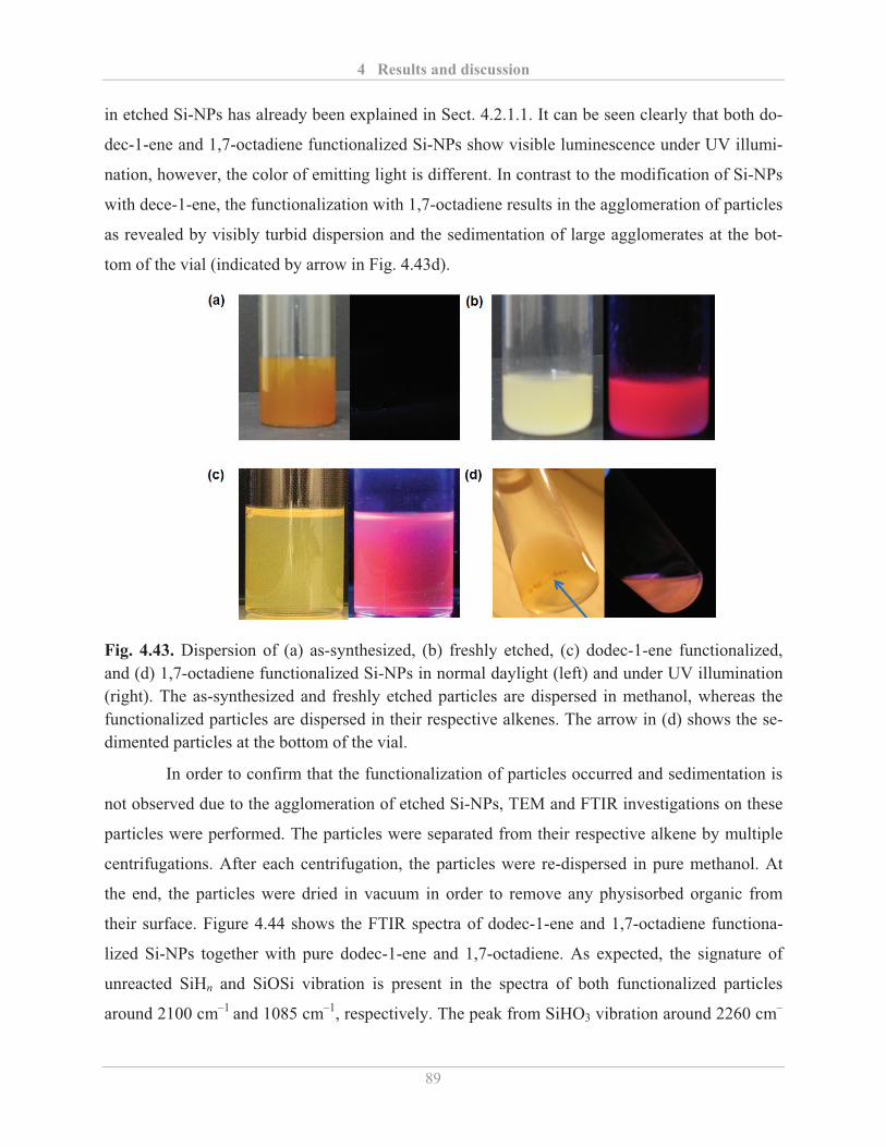
4 Results and discussion
89
in etched Si-NPs has already been explained in Sect. 4.2.1.1. It can be seen clearly that both do-
dec-1-ene and 1,7-octadiene functionalized Si-NPs show visible luminescence under UV illumi-
nation, however, the color of emitting light is different. In contrast to the modification of Si-NPs
with dece-1-ene, the functionalization with 1,7-octadiene results in the agglomeration of particles
as revealed by visibly turbid dispersion and the sedimentation of large agglomerates at the bot-
tom of the vial (indicated by arrow in Fig. 4.43d).
Fig. 4.43. Dispersion of (a) as-synthesized, (b) freshly etched, (c) dodec-1-ene functionalized, and (d) 1,7-octadiene functionalized Si-NPs in normal daylight (left) and under UV illumination (right). The as-synthesized and freshly etched particles are dispersed in methanol, whereas the functionalized particles are dispersed in their respective alkenes. The arrow in (d) shows the se-dimented particles at the bottom of the vial.
In order to confirm that the functionalization of particles occurred and sedimentation is
not observed due to the agglomeration of etched Si-NPs, TEM and FTIR investigations on these
particles were performed. The particles were separated from their respective alkene by multiple
centrifugations. After each centrifugation, the particles were re-dispersed in pure methanol. At
the end, the particles were dried in vacuum in order to remove any physisorbed organic from
their surface. Figure 4.44 shows the FTIR spectra of dodec-1-ene and 1,7-octadiene functiona-
lized Si-NPs together with pure dodec-1-ene and 1,7-octadiene. As expected, the signature of
unreacted SiHn and SiOSi vibration is present in the spectra of both functionalized particles
around 2100 cm–1 and 1085 cm–1, respectively. The peak from SiHO3 vibration around 2260 cm–
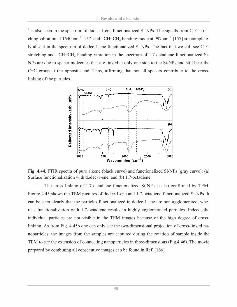
4 Results and discussion
90
1 is also seen in the spectrum of dodec-1-ene functionalized Si-NPs. The signals from C=C stret-
ching vibration at 1640 cm–1 [157] and –CH=CH2 bending mode at 997 cm–1 [157] are complete-
ly absent in the spectrum of dodec-1-ene functionalized Si-NPs. The fact that we still see C=C
stretching and –CH=CH2 bending vibration in the spectrum of 1,7-octadiene functionalized Si-
NPs are due to spacer molecules that are linked at only one side to the Si-NPs and still bear the
C=C group at the opposite end. Thus, affirming that not all spacers contribute to the cross-
linking of the particles.
Fig. 4.44. FTIR spectra of pure alkene (black curve) and functionalized Si-NPs (gray curve): (a) Surface functionalization with dodec-1-ene, and (b) 1,7-octadiene.
The cross linking of 1,7-octadiene functionalized Si-NPs is also confirmed by TEM.
Figure 4.45 shows the TEM pictures of dodec-1-ene and 1,7-octadiene functionalized Si-NPs. It
can be seen clearly that the particles functionalized in dodec-1-ene are non-agglomerated, whe-
reas functionalization with 1,7-octadiene results in highly agglomerated particles. Indeed, the
individual particles are not visible in the TEM images because of the high degree of cross-
linking. As from Fig. 4.45b one can only see the two-dimensional projection of cross-linked na-
noparticles, the images from the samples are captured during the rotation of sample inside the
TEM to see the extension of connecting nanoparticles in three-dimensions (Fig.4.46). The movie
prepared by combining all consecutive images can be found in Ref. [166].
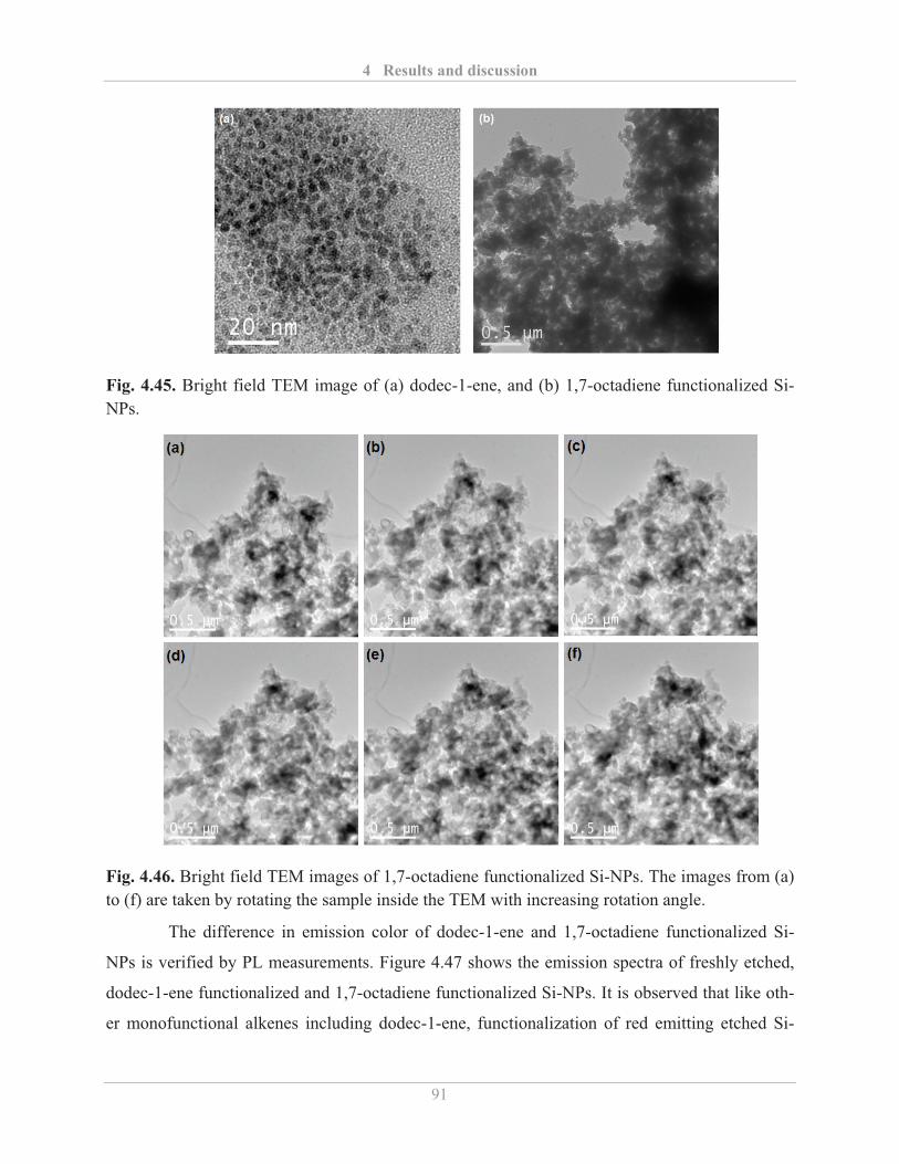
4 Results and discussion
91
Fig. 4.45. Bright field TEM image of (a) dodec-1-ene, and (b) 1,7-octadiene functionalized Si-NPs.
Fig. 4.46. Bright field TEM images of 1,7-octadiene functionalized Si-NPs. The images from (a) to (f) are taken by rotating the sample inside the TEM with increasing rotation angle.
The difference in emission color of dodec-1-ene and 1,7-octadiene functionalized Si-
NPs is verified by PL measurements. Figure 4.47 shows the emission spectra of freshly etched,
dodec-1-ene functionalized and 1,7-octadiene functionalized Si-NPs. It is observed that like oth-
er monofunctional alkenes including dodec-1-ene, functionalization of red emitting etched Si-
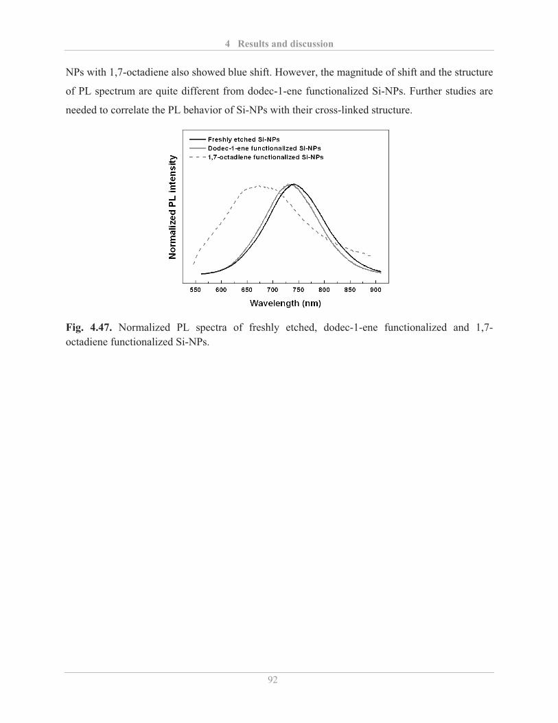
4 Results and discussion
92
NPs with 1,7-octadiene also showed blue shift. However, the magnitude of shift and the structure
of PL spectrum are quite different from dodec-1-ene functionalized Si-NPs. Further studies are
needed to correlate the PL behavior of Si-NPs with their cross-linked structure.
Fig. 4.47. Normalized PL spectra of freshly etched, dodec-1-ene functionalized and 1,7-octadiene functionalized Si-NPs.
5 Summary and conclusions
93
5 Summary and conclusions
The discovery of efficient light emission from nanocrystalline silicon compared to bulk opened
up the possibility to develop optoelectronic devices based on silicon [12, 167, 168]. However, it
is observed that silicon is very prone to oxidation in the presence of air, which deteriorates its
optical and electrical properties [25, 38-40]. To prevent oxidation, the surface of silicon can be
passivated with organic molecules through Si-C bonds [78]. As surface plays a very important
role in governing the properties of nanoparticles, modification of silicon nanoparticles (Si-NPs)
surface may alter their properties. Therefore, a high technological interest exists to understand
the influence of surface modification on the optical, electrical, and dispersion properties of Si-
NPs for the realization of silicon based printable optoelectronic devices.
The main objective of the present work was to study the influence of surface modifica-
tion on the optical, electrical and dispersion properties of Si-NPs. During this research, several
interesting properties were explored, which are broadly associated with the surface chemistry of
Si-NPs and defects on their surface. The results obtained in present research are briefly summa-
rized below.
The Si-NPs, investigated in this thesis, are synthesized in a low-pressure microwave
plasma reactor via pyrolysis of SiH4. The as-synthesized particles are highly crystalline in nature
and showed the presence of an amorphous oxide layer on their surface due to oxidation of par-
ticles in air. Additionally, due to collision of particles inside the reactor and surface oxidation of
particles outside the reaction chamber, significant agglomeration of particles is seen. The surface
of as-synthesized Si-NPs is passivated with organic molecules by etching them in hydrofluoric
acid (HF) and subsequent surface functionalization with alkenes. Nearly complete removal of
oxides from the surface of Si-NPs is observed after HF etching. TEM images showed that func-
tionalization particles are mostly non-agglomerated, indicating that etching and functionalization
processes resolve the agglomeration of Si-NPs.
5 Summary and conclusions
94
It is observed that the as-synthesized Si-NPs with oxide layer have a high concentration
of dangling bonds on their surface. The presence of these dangling bonds suppresses the radia-
tive recombination of excitons and as a result as-synthesized Si-NPs show very weak photolumi-
nescence (PL). A strong decrease in the dangling bond concentration of as-synthesized Si-NPs is
observed after etching them with HF. This causes an increase in their PL intensity approximately
by a factor of 20. It is seen that the etching of as-synthesized Si-NPs also contributes to a small
blue shift in their spectrum (�� = 36 nm). With increased etching of Si-NPs in a mixture of HF
and HNO3, a shift of the PL emission from red to green is obtained. This confirmed that red to
green PL emission of Si-NPs is due to quantum confinement effects. The blue emission cannot
obtained from further etching. It is found that surface oxidation of Si-NPs almost completely
quenches the PL emission of most of Si-NPs after some time, which compares well with pre-
vious observations [25, 169]. However, during the oxidation of orange luminescing Si-NPs, ma-
terial with blue photoluminescence is formed while the orange emission disappears. The peak of
blue luminescence did not change its position during the oxidation and an increase in the PL in-
tensity with increasing oxidation time is seen. These results indicate that the blue luminescence
originates from defect states and not from the quantum confinement.
The stability of Si-NPs against surface oxidation was also examined in this study. The
functionalized Si-NPs showed higher stability in air compared to freshly etched Si-NPs. Howev-
er, incomplete surface coverage of Si-NPs with organic molecules limits their long-term stability.
The particles functionalized with different organic substances showed different surface coverage
and thus difference in long-term stability in air. The functionalization of Si-NPs using thermally
induced hydrosilylation gives the best surface coverage with dodec-1-ene among all n-alkenes.
The optimum temperature and time for the surface functionalization is found to be 120°C and 10
h. The Si-NPs terminated with ester groups showed higher stability against oxidation in air com-
pared to dodec-1-ene. Additionally, it is seen that the use of reactants with bulky organic groups
further decreases the oxidation susceptibility of the particles.
The functionalized Si-NPs show bright and stable PL for months (visible inspection).
Also, the functionalized Si-NPs show high quantum yield (~15%). However, it is seen that func-
tionalization process does not stabilize the original luminescence from freshly etched Si-NPs.
The particles emitting in orange to red and yellow to green regime show a blue and red shift after
5 Summary and conclusions
95
their surface functionalization, respectively. It is observed that the magnitude of the spectral shift
can be altered by changing the coverage of organic molecules on the Si-NPs surface. The par-
ticles with high surface coverage show higher shift compared to particles with low surface cov-
erage. Because a high surface coverage of organic molecules is needed to generate Si-NPs with
long-term stability, materials that emit in the red to yellow range can be stabilized with this
process, but stable materials with green emission are not achieved due to switching of the nature
of shift (red/blue) in the orange-yellow region. Stable blue emission is obtained from the oxida-
tion of orange emitting etched Si-NPs.
The electrical conductivity of as-synthesized Si-NPs (dp ~ 52 nm) is found to be very
low (� ~ 10–7 �–1cm–1 at 100°C). Etching of particles with HF increases their electrical conduc-
tivity by four orders of magnitude (� ~ 10–3 �–1cm–1 at 100°C). However, the freshly etched Si-
NPs do not show stable conductivity in air due to surface oxidation. A decrease in the electrical
conductivity of etched Si-NPs is seen with increasing oxidation time. The conductivity of oxi-
dized Si-NPs is found to be higher than as-synthesized samples even after six months of expo-
sure to air. It is observed that the functionalization of freshly etched Si-NPs also decreases their
electrical conductivity. Additionally, the conductivity of functionalized Si-NPs can be tuned by
changing the length of organic ligands. Among all n-alkenes, the functionalization of Si-NPs
with dodec-1-ene exhibits the highest conductivity. Furthermore, the electrical conductivity of
dodec-1-ene functionalized Si-NPs is found to be very stable in air.
It is seen that the stability of as-synthesized Si-NPs dispersion is limited due to the pres-
ence of big agglomerates and surface oxides. Etching and functionalization of Si-NPs causes the
de-agglomeration of particles and the presence of organic molecules allows them to form stable
dispersion in a variety of organic solvents. The stable dispersion of functionalized Si-NPs is used
to print structure on glass substrate.
For the cross-linking of Si-NPs, functionalization of particle surface with bifunctional
organic molecules is proposed. The bifunctional organic molecules can be bonded to the particles
through both functional groups and therefore can cause a cross-linked network. In this work,
successful cross-linked Si-NPs structure is accomplished by functionalization of particles using
1,7-octadiene.
5 Summary and conclusions
96
In conclusion, the inadequacy of PL stability, poor electrical property and limited num-
ber of choice of dispersion medium for as-synthesized Si-NPs preclude them for practical appli-
cations. The etched Si-NPs show improved optical and electrical properties, however, these par-
ticles are not stable in air due to surface oxidation. In contrast, the functionalized Si-NPs show
very good and stable photoluminescence, electrical, and dispersion properties. Therefore, they
are a good candidates for future printable optoelectronic device applications.
The present research work provides a path for the production of highly stable Si-NPs
ink with tunable optical and electrical properties, and paves the way for the application of silicon
based low cost printable optoelectronics.
6 Recommendations for future work
97
6 Recommendations for future work
The knowledge gained from this work can be utilized to extend the research in Si-NPs in various
directions. Some of the research recommendations are listed below.
As discussed in this thesis, the PL emission of functionalized Si-NPs can be tuned by
changing the organic ligands on their surface. In future, the effect of organic ligands on the PL
life time and quantum yield can be examined. Additionally, it has been observed that the quan-
tum yield of CdSe/ZnSe core-shell structures capped with organic molecules depends on the
length of organic ligands on their surface [170]. If similar effects are observed in Si-NPs, par-
ticles with improved quantum yields can be prepared.
In this work, it was found that the electrical conductivity of Si-NPs can be tuned by
changing the functional group on their surface. Additionally, it was demonstrated that Si-NPs
can be cross linked to each other using bifunctional organic molecules. The cross linking of Si-
NPs could result in the enhanced electrical conductivity compared to particles that are not linked
to each other, as then the electrons do not have to cross the tunneling barrier while moving from
one particle to another. The use of conductive spacer layers can further enhance the electron
transport between particles. Furthermore, the use of connecting molecules with different spacer
length can also influences the electrical conductivity of cross-linked particles. It would be inter-
esting to explore all these features.
In the research presented here, it was shown that highly stable ink from functionalized Si-
NPs with tunable optical and electrical properties can be prepared. Additionally, it was shown
that these particles can be used to print the structures on a substrate. It is known from literature
that the morphology of deposited particles depends on various factors, such as particle concentra-
tion and choice of the dispersion medium [165]. Because the performance of a printed device
depends on the quality of the printed layer, the optimization of different parameters influencing

6 Recommendations for future work
98
the quality of the printed layer is very important. These studies need to be performed in future for
the realization of Si-NPs based printable optoelectronic devices.
7 References
99
7 References
1. C. N. Rao; G. U. Kulkarni; P. J. Thomas; P. P. Edwards, Size-dependent chemistry: Properties of nanocrystals. Chem. Eur. J. 2002, 8, 28.
2. M. Hirasawa; T. Orii; T. Seto, Size-dependent crystallization of Si nanoparticles. Appl. Phys. Lett. 2006, 88, 093119.
3. R. Waser, Nanoelectronics and information technology. Wiley VCH 2003.
4. Nanoscience and nanotechnologies: Opportunities and uncertainties. The Royal Society & The Royal Academy of Engineering, Nanoscience and Nanotechnologies July 2004.
5. Higher-capacity lithium-ion batteries. Technology Review June 22, 2006.
6. Discovery and applications of photocatalysis — Creating a comfortable future by making use of light energy. Japan Nanonet Bulletin May 12, 2005.
7. Nanotechnology: Enabling technologies for Australian innovative industries. Paper pre-pared by an independent working group for the Prime Minister’s Science, Engineering and Innovation Council (PMSEIC), Australian Government. 11 March, 2005.
8. ScienceDaily, New nanotechnology products hitting the market at the rate of 3-4 per week. April 25, 2008.
9. M. Jaroniec, Silicon beyond the valley. Nat. Chem. 2009, 1, 166.
10. S. Niesar; R. Dietmueller; H. Nesswetter; H. Wiggers; M. Stutzmann, Silicon/organic semiconductor heterojunctions for solar cells. Phys. Status Solidi A 2009, 206, 2775.
11. C.-Y. Liu; Z. C. Holman; U. R. Kortshagen, Hybrid solar cells from P3HT and silicon nanocrystals. Nano Lett. 2009, 9, 449.
12. L. Canham, Gaining light from silicon. Nature 2000, 408, 411.
13. N. M. Park; T. S.Kim; S. J. Park, Band gap engineering of amorphous silicon quantum dots for light-emitting diodes. Appl. Phys. Lett. 2001, 78, 2575.
14. F. Erogbogbo; K. T. Yong; I. Roy; G. Xu; P. N. Prasad; M. T. Swihart, Biocompatible luminescent silicon quantum dots for imaging of cancer cells. ACS Nano 2008, 2, 873.
15. T. S.-Iwayama; S. Nakao; K. Saitoh, Visible photoluminescence in Si+ implanted ther-mal oxide films on crystalline Si. Appl. Phys. Lett. 1994, 65, 1814.
7 References
100
16. T. S.-Iwayama; K. Fujita; S. Nakao; K. Saitoh; T. Fujita; N. Itoh, Visible photolumines-cence in Si+ implanted silica glass. J. Appl. Phys. 1994, 75, 7779.
17. T. S.-Iwayama; S. Nakao; K. Saitoh; N. Itoh, Photoluminescence from nanoparticles of silicon embedded in an amorphous silicon dioxide matrix. J. Phys. Condens. Matter 1994, 6, L601.
18. J. Zou; R. K. Baldwin; K. A. Pettigrew; S. M. Kauzlarich, Solution synthesis of ultrasta-ble luminescent siloxane-coated silicon nanoparticles. Nano Lett. 2004, 4, 1181.
19. J. P. Wilcoxon; G. A. Samara, Tailorable, visible light emission from silicon nanocrys-tals. Appl. Phys. Lett. 1999, 74, 3164.
20. J. P. Wilcoxon; G. A. Saara; P. N. Provencio, Optical and electronic properties of Si na-noclusters synthesized in inverse micelles. Phys. Rev. B 1999, 60, 2704.
21. J. R. Heath, A liquid-solution-phase synthesis of crystalline silicon. Science 1992, 258, 1131.
22. R. A. Bley; S. M. Kauzlarich, A low-temperature solution phase route for the synthesis of silicon nanoclusters. J. Am. Chem. Soc. 1996, 118, 12461.
23. R. D. Tilley ; J. H. Warner; K. Yamamoto; I. Matsui; H. Fujimori, Micro-emulsion syn-thesis of monodisperse surface stabilized silicon nanocrystals. Chem. Commun. 2005, 1833.
24. J. H. Warner; A. Hoshino; K. Yamamoto; R. D. Tilley, Water-soluble photoluminescent silicon quantum dots. Angew. Chem. Int. Ed. 2005, 117, 4626.
25. X. Li; Y. He; S. S. Talukdar; M. T. Swihart, Process for preparing macroscopic quantities of brightly photoluminescent silicon nanoparticles with emission spanning the visible spectrum. Langmuir 2003, 19, 8490.
26. L. Mangolini, Non-thermal plasma synthesis and passivation of luminescent silicon na-nocrystals. University of Minnesota 2007.
27. B. Gelloz; A. Kojima; N. Koshida, Highly efficient and stable luminescence of nanocrys-talline porous silicon treated by high-pressure water vapor annealing. Appl. Phys. Lett. 2005, 87, 031107.
28. X. D. Pi; L. Mangolini; S. A. Campbell; U. Kortshagen, Room-temperature atmospheric oxidation of Si nanocrystals after HF etching. Phy. Rev. B 2007, 75, 085423.
29. C. Garcia; B. Garrido; P. Pellegrino; R. Ferre; J. A. Moreno; J. R. Morante; L. Pavesi; M. Cazzanelli, Size dependence of lifetime and absorption cross section of Si nanocrystals embedded in SiO2. Appl. Phys. Lett. 2003, 82, 1595.
30. D. I. Kovalev; I. D. Yaroshetzkii; T. Muschik; V. P. Koch; F. Koch, Fast and slow visible luminescence bands of oxidized porous Si. Appl. Phys. Lett. 1994, 64, 214.
7 References
101
31. Z. Kang; Y. Liu; C. H. A. Tsang; D. D. D. Ma; X. Fan; N. Wong; S. Lee, Water-soluble silicon quantum dots with wavelength-tunable photoluminescence. Adv. Fun. Mater. 2009, 21, 661.
32. M. V. Wolkin; J. Jorne; P. M. Fauchet; G. Allan; C. Delerue, Electronic states and lumi-nescence in porous silicon quantum dots: The role of oxygen. Phys. Rev. Lett. 1999, 82, 197.
33. H. Mizuno; H. Koyama; N. Koshida, Oxide-free blue photoluminescence from photo-chemically etched porous silicon. Appl. Phys. Lett. 1996, 69, 3779.
34. Q. Chen; X. J. Li; Y. B. Jia; J. S. Zhu; Z. Yuheng, The role of SiO2 in the blue lumines-cence in hydrothermally prepared porous silicon. J. Phys.: Condens. Matter 1997, 9, L151.
35. M. Zhu; G. Chen; P. Chen, Green/blue light emission and chemical feature of nanocrys-talline silicon embedded in silicon-oxide thin film. Appl. Phys. A 1997, 65, 195.
36. Y. S. Kim; K. Y. Suh; H. Yoon; H. H. Lee, Stable blue photoluminescence from porous silicon. J. Electrochem. Soc. 2002, 149, C50.
37. X. Li; Y. He; M. T. Swihart, Surface functionalization of silicon nanoparticles produced by laser-driven pyrolysis of silane followed by HF-HNO3 etching. Langmuir 2004, 20, 4720.
38. A. R. Stegner; R. N. Pereira; K. Klein; R. Lechner; R. Dietmueller; M. S. Brandt; M. Stutzmann; H. Wiggers, Electronic transport in phosphorus-doped silicon nanocrystal networks. Phys. Rev. Lett. 2008, 100, 026803.
39. L. Gilles; G. Jiong; H. Friedrich, Effect of passivation and aging on the photolumines-cence of silicon nanocrystals. Appl. Phys. Lett. 2001, 79, 4028.
40. J. Nelles; D. Sendor; F.-M. Petrat; U. Simon, Electrical properties of surface functiona-lized silicon nanoparticles. J. Nanopart. Res. 2010, 12, 1367.
41. M. A. Brook, Silicon in organic, organometallic, and polymer chemistry. Wiley: New York 2000.
42. S. Patai; Z. Rappoport, The chemistry of organic silicon compound. John Wiley and Sons: New York 1989.
43. M. R. Linford; P. Fenter; P. M. Eisenberger; C. E. D. Chidsey, Alkyl monolayers on sili-con prepared from 1-alkenes and hydrogen-terminated silicon. J. Am. Chem. Soc. 1995, 117, 3145.
44. B. Fabre; G. P. Lopinski; D. D. M. Wayner, Functionalization of Si(111) surfaces with alkyl chains terminated by electrochemically polymerizable thienyl units. Chem. Com-mun. 2002, 2904.
7 References
102
45. J. M. Buriak; M. P. Stewart; T. W. Geders; M. J. Allen; H. C. Choi; J. Smith; D. Raftery; L. T. Canham, Lewis acid mediated hydrosilylation on porous silicon surfaces. J. Am. Chem. Soc. 1999, 121, 11491.
46. R. Boukherroub; S. Morin; D. D. M. Wayner; D. J. Lockwood, Thermal route for chemi-cal modification and photoluminescence stabilization of porous silicon. Phys. Status So-lidi A 2000, 182, 117.
47. R. Boukherroub; S. Morin; P. Sharpe; D. D. M. Wayner, Insights into the formation me-chanisms of Si�OR monolayers from the thermal reactions of alcohols and aldehydes with Si(111)�H. Langmuir 2000, 16, 7429.
48. R. Boukherroub; D. D. M. Wayner, Controlled functionalization and multistep chemical manipulation of covalently modified Si(111) surfaces. J. Am. Chem. Soc. 1999, 121, 11513.
49. J. M. Schmeltzer; L. A. Porter; M. P. Stewart; J. M. Buriak, Hydride abstraction initiated hydrosilylation of terminal alkenes and alkynes on porous silicon. Langmuir 2002, 18, 2971.
50. M. P. Stewart; J. M. Buriak, Exciton-mediated hydrosilylation on photoluminescent na-nocrystalline silicon. J. Am. Chem. Soc. 2001, 123, 7821.
51. J. M. Buriak; M. J. Allen, Lewis acid mediated functionalization of porous silicon with substituted alkenes and alkynes. J. Am. Chem. Soc. 1998, 120, 1339.
52. J. Nelles; D. Sendor; A. Ebbers; F. Petrat; H. Wiggers; C. Schulz; U. Simon, Functionali-zation of silicon nanoparticles via hydrosilylation with 1-alkenes. Colloid. Polym. Sci. 2007, 285, 729.
53. F. A. Reboredo; G. Galli, Theory of alkyl-terminated silicon quantum dots. J. Phys. Chem. B 2005, 109, 1072.
54. H. H. Lee; K. S. Chou; K. C. Huang, Inkjet printing of nanosized silver colloids. Nano-tech. 2005, 16, 2436.
55. C. Ingrosso; J. Y. Kim; E. Binetti; V. Fakhfouri; M. Striccoli; A. Agostiano; M. L. Curri; J. Brugger, Drop-on-demand inkjet printing of highly luminescent CdS and CdSe@ZnS nanocrystal based nanocomposites. Microelectron. Eng. 2009, 86, 1124.
56. W. Cui; W. Lu; Y. Zhang; G. Lin; T. Wei; L. Jiang, Gold nanoparticle ink suitable for electric-conductive pattern fabrication using in ink-jet printing technology. Colloids Surf. A 2007, 358, 35.
57. I.-K. Shim; Lee, Y.; K. J.Lee; J. Joung, An organometallic route to highly monodispersed silver nanoparticles and their application to ink-jet printing. Mater. Chem. Phys. 2008, 110, 316.
58. H.-W. Lin; W.-H. Hwu; M.-D. Ger, The dispersion of silver nanoparticles with physical dispersal procedures. J. Mater. Process. Technol. 2008, 206, 56.
7 References
103
59. H.-H. Lee; Chou, K.-S.; Huang, K.-C., Inkjet printing of nanosized silver colloids. Nano-tech. 2005, 16, 2436.
60. M. Harting; J. Zhang; D. R. Gamota; D. T. Britton, Fully printed silicon field effect tran-sistors. Appl. Phys. Lett. 2009, 94, 193509.
61. U. Simon; R. Flesch; H. Wiggers; G. Schön; G. Schmid, Chemical tailoring of the charg-ing energy in metal cluster arrangements by use of bifunctional spacer molecules J. Ma-ter. Chem. 1998, 8, 517.
62. M. Brust; D. Bethell; D. J. Schiffrin; C. J. Kiely, Novel gold-dithiol nano-networks with non-metallic electronic properties. Adv. Mater. 1995, 7, 795.
63. J. J. Storhoff; A. A. Lazarides; R. C. Mucic; C. A. Mirkin; R. L. Letsinger; G. C. Schatz, What controls the optical properties of DNA-linked gold nanoparticle assemblies? J. Am. Chem. Soc. 2000, 122, 4640.
64. H. Bönnemann; N. Waldofner; H. G. Haubold; T. Vad, Preparation and characterization of three-dimensional Pt nanoparticle networks. Chem. Mater. 2002, 14, 1115.
65. L. Pavesi; D. J. Lockwood, Silicon photonic. Springer 2004.
66. L. T. Canham, Silicon quantum wire array fabrication by electrochemical and chemical dissolution of wafers. Appl. Phys. Lett. 1990, 57, 1046.
67. L. T. Canham, Luminescence bands and their proposed origins in highly porous silicon. Phys. Status Solidi B 1995, 190, 9.
68. L. T. Canham; M. R. Houlton; W. Y. Leong; C. Pickering; J. M. Keen, Atmospheric im-pregnation of porous silicon at room temperature. J. Appl. Phys. 1991, 70, 422.
69. A. G. Cullis; L. T. Canhan, Visible light emission due to quantum size effects in highly porous crystalline silicon. Nature 1991, 353, 335.
70. V. Lehmann; U. Gösele, Porous silicon formation: A quantum wire effect. Appl. Phys. Lett. 1991, 58, 856.
71. S. Veprek, Electronic and mechanical properties of nanocrystalline composites when ap-proaching molecular size. Thin Solid Films 1997, 297, 145.
72. Z.Kang; Y. Liu; C. H. A. Tsang; D. D. D. Ma; X. Fan; N. Wong; S. Lee, Water-soluble silicon quantum dots with wavelength-tunable photoluminescence. Adv. Fun. Mater. 2009, 21, 661.
73. M. Dovrat; N. Arad; X. H. Zhang; S. T. Lee; A. Sa'ar, Cathodoluminescence and photo-luminescence of individual silicon nanowires. Phys. Status Solidi A 2007, 204, 1512.
74. J. S. Biteen; D. Pacifici; N. S. Lewis; H. A. Atwater, Enhanced radiative emission rate and quantum efficiency in coupled silicon nanocrystal-nanostructured gold emitters. Na-no Lett. 2005, 5, 1768.
7 References
104
75. R. J. Walters; J. Kalkman; A. Polman; H. A. Atwater; M. J. A. de Dood, Photolumines-cence quantum efficiency of dense silicon nanocrystal ensembles in SiO2. Phys. Rev. B 2006, 73, 132302.
76. L. Gilles; G. Jiong; H. Friedrich, Effect of passivation and aging on the photolumines-cence of silicon nanocrystals. Appl. Phys. Lett. 2001, 79, 4028.
77. A. R. Stegner; R. N. Pereira; R. Lechner; K. Klein; H. Wiggers; M. Stutzmann; M. S. Brandt, Doping efficiency in freestanding silicon nanocrystals from the gas phase: Phos-phorus incorporation and defect-induced compensation. Phys. Rev. B 2009, 80, 165326.
78. F. Hua; M. T. Swihart; E. Ruckenstein, Efficient surface grafting of luminescent silicon quantum dots by photoinitiated hydrosilylation. Langmuir 2005, 21, 6054.
79. J. Nelles; D. Sendor; M. Bertmer; A. Ebbers; F. M. Petrat; U. Simon, Surface chemistry of n-octane modified silicon nanoparticles analysed by IR, 13C CPMAS NMR and EELS. J. Nanosci. Nanotechnol. 2007, 7, 2818.
80. R. Lechner; A. R. Stegner; R. N. Pereira; R. Dietmueller; M. S. Brandt; A. Ebbers; M. Trocha; H. Wiggers; M. Stutzmann, Electronic properties of doped silicon nanocrystal films. J. Appl. Phys. 2008, 104, 053701.
81. H. Sirringhaus; T. Kawase; R. H. Friend; T. Shimoda; M. Inbasekaran; W. Wu; E. P. Woo, High-resolution inkjet printing of all-polymer transistor circuits. Science 2000, 290, 2123.
82. C. �N. Hoth; S. �A. Choulis; P. Schilinsky; C. �J. Brabec, High photovoltaic performance of inkjet printed polymer: Fullerene blends. Adv. Mater. 2007, 19, 3973.
83. V. Wood; M. J. Panzer; J. Chen; M. S. Bradley; J. E. Halpert; M. G. Bawendi; V. Bulovi�, Inkjet-printed quantum dot–polymer composites for full-color AC-driven dis-plays. Adv. Mater. 2009, 21, 2151.
84. L. Mangolini; U. Kortshagen, Plasma-assisted synthesis of silicon nanocrystal inks. Adv. Mater. 2007, 19, 2513.
85. M. T. Swihart, Silicon nanoparticles: Vapor-phase synthesis of nanoparticles. Curr. Opin. Colloid Interface Sci. 2003, 8, 127.
86. B. Schwade; P. Roth, Simulation of nano-particle formation in a wall-heated aerosol reactor including coalescence. J. Aerosol Sci. 2003, 34, 339.
87. B. Giesen; H. Wiggers; A. Kowalik; P. Roth, Formation of Si-nanoparticles in a micro-wave reactor: Comparison between experiments and modelling J. Nanopart. Res. 2005, 7, 29.
88. D. Woiki; A. Kunz; P. Roth, Chemical reactions of aerosol precursors. J. Aerosol Sci. Suppl. 2000, 1, 212.
7 References
105
89. J. E. McDonald, Homogeneous nucleation of vapor condensation. II. Kinetic aspects. Am. J. Phys. 1963, 31, 31.
90. W. C. Hinds, Aerosol technology: Properties, behavior, and measurement of airborne particles. Wiley-Interscience 1999.
91. M. Winterer, Nanocrystalline ceramics - Synthesis and structure. Springer 2002.
92. S. Tsantilis; S. E. Pratsinis, Soft- and hard-agglomerate aerosols made at high tempera-tures. Langmuir 2004, 20, 5933.
93. IUPAC, Stability constants of metal ion complexes: Part A. Pergamon Press: Oxford 1982.
94. L. J. Warren, The measurement of pH in acid fluoride solutions and evidence for the exis-tence of (HF)2. Anal. Chim. Acta 1971, 53, 199.
95. D. M. Knotter, Etching mechanism of vitreous silicon dioxide in HF-based solutions. J. Am. Chem. Soc. 2000, 122, 4345.
96. G. W. Trucks; K. Raghavachari; G. S. Higashi; Y. J. Chabal, Mechanism of HF etching of silicon surfaces: A theoretical understanding of hydrogen passivation. Phys. Rev. Lett. 1990, 65, 504.
97. E. Sacher; A. Yelon, Comment on ``Mechanism of HF etching of silicon surfaces: A theoretical understanding of hydrogen passivation''. Phys. Rev. Lett. 1991, 66, 1647.
98. J. Fritz; E. B. Cooper; S. Gaudet; P. K. Sorger; S. R. Manalis, Electronic detection of DNA by its intrinsic molecular charge. Proc. Natl. Acad. Sci. 2002, 99, 14142.
99. A. B. Sieval; A. L. Demirel; J. W. M. Nissink; M. R. Linford; J. H. van der Maas; W. H. de Jeu; H. Zuilhof; E. J. R. Sudhölter, Highly stable Si-C linked functionalized monolay-ers on the silicon (100) surface. Langmuir 1998, 14, 1759.
100. T. Strother; W. Cai; X. Zhao; R. J. Hamers; L. M. Smith, Synthesis and characterization of DNA-modified silicon (111) surfaces. J. Am. Chem. Soc. 2000, 122, 1205.
101. T. He; J. He; M. Lu; B. Chen; H. Pang; W. F. Reus; W. M. Nolte; D. P. Nackashi; P. D. Franzon; J. M. Tour, Controlled modulation of conductance in silicon devices by molecu-lar monolayers. J. Am. Chem. Soc. 2006, 128, 14537.
102. R. C. Anderson; R. S. Muller; C. W. Tobias, Chemical surface modification of porous silicon. J. Electrochem. Soc. 1993, 140, 1393.
103. V. M. Dubin; C. Vieillard; F. Ozanam; J. N. Chazalviel, Preparation and characterization of surface-modified luminescent porous silicon. Phys. Status Solidi B 1995, 190, 47.
104. J. M. Buriak, Organometallic chemistry on silicon and germanium surfaces. Chem. Rev. 2002, 102, 1271.
7 References
106
105. L. C. P. M. de Smeta; A. V. Pukina; Q.-Y. Suna; B. J. Evesb; G. P. Lopinskib; G. M. Vissera; H. Zuilhofa; E. J. R. Sudhöltera, Visible-light attachment of Si-C linked functio-nalized organic monolayers on silicon surfaces. Appl. Surf. Sci. 2005, 252, 24.
106. L. C. P. M. de Smet; H. Zuilhof; E. J. R. Sudhölter; L. H. Lie; A. Houlton; B. R. Hor-rocks, Mechanism of the hydrosilylation reaction of alkenes at porous silicon: Experi-mental and computational deuterium labeling studies. J. Phys. Chem. B 2005, 109, 12020.
107. N. Y. Kim; P. E. Laibinis, Derivatization of porous silicon by grignard reagents at room temperature. J. Am. Chem. Soc. 1998, 120, 4516.
108. S. B. Fuller, A fast flexible ink-jet printing method for patterning networks of neurons in culture. Massachusetts Institute of Technology 2000.
109. L. Lutterotti; S. Matthies; H. R. Wenk, MAUD: A friendly Java program for material analysis using diffraction. ICUr: Newsletter of the CPD 1999, 21, 14. Program available at http://www.ing.unitn.it/~maud/.
110. U. Kaiser, Characterisation of thin SiC films and low-dimensional structures in SiC using advanced transmission electron microscopy. Friedrich Schiller University of Jena 2002.
111. E. Barsoukov; J. R. Macdonald, Impedance spectroscopy: theory, experiment, and appli-cations. Wiley-InterScience 2005.
112. H. Günzler; H.-U. Gremlich, IR spectroscopy: An introduction. Wiley-VCH 2002.
113. M. Brustolon; E. Giamello, Electron paramagnetic resonance: A practitioners toolkit. Wiley InterScience 2009.
114. C. Meier; A. Gondorf; S. Luttjohann; A. Lorke; H. Wiggers, Silicon nanoparticles: Ab-sorption, emission, and the nature of the electronic bandgap. J. Appl. Phys. 2007, 101, 103112.
115. M. S. Hybertsen, Absorption and emission of light in nanoscale silicon structures. Phys. Rev. Lett. 1994, 72, 1514.
116. G. Allan; C. Delerue; M. Lannoo, Nature of luminescent surface states of semiconductor nanocrystallites. Phys. Rev. Lett. 1996, 76, 2961.
117. J. Valenta; R. Juhasz; J. Linnros, Photoluminescence spectroscopy of single silicon quan-tum dots. Appl. Phys. Lett. 2002, 80, 1070.
118. K. Kimura, Blue luminescence from silicon nanoparticles suspended in organic liquids. J. Cluster Sci. 1999, 10, 359.
119. C. Delerue; G. Allan; M. Lannoo, Theoretical aspects of the luminescence of porous sili-con. Phys. Rev. B 1993, 48, 11024.
7 References
107
120. G. Ledoux; O. Guillois; D. Porterat; C. Reynaud; F. Huisken; B. Kohn; V. Paillard, Pho-toluminescence properties of silicon nanocrystals as a function of their size. Phys. Rev. B 2000, 62, 15942.
121. L. Mangolini; D. Jurbergs; E. Rogojina; U. Kortshagen, Plasma synthesis and liquid-phase surface passivation of brightly luminescent Si nanocrystals. J. Lumin. 2006, 121, 327.
122. J. Knipping; H. Wiggers; B. Rellinghaus; P. Roth; D. Konjhodzic; C. Meier, Synthesis of high purity silicon nanoparticles in a low pressure microwave reactor. J. Nanosci. Nano-technol. 2004, 4, 1039.
123. A. Weibel; R. Bouchet; F. Boulc'h; P. Knauth, The big problem of small particles: A comparison of methods for determination of particle size in nanocrystalline anatase powders. Chem. Mater. 2005, 17, 2378.
124. G. Lucovsky; R. J. Nemanich; J. C. Knights, Structural interpretation of the vibrational spectra of a-Si: H alloys. Phy. Rev. B 1979, 19, 2064.
125. G. J. Kluth; M. Roya, Oxidation mechanism of the ammonium-fluoride-treated Si(100) surface. J. Appl. Phys. 1996, 80, 5408.
126. G. Lucovsky; J. Yang; S. S. Chao; J. E. Tyler; W. Czubatyj, Oxygen-bonding environ-ments in glow-discharge-deposited amorphous silicon-hydrogen alloy films. Phy. Rev. B 1983, 28, 3225.
127. P. G. Pai; S. S. Chao; Y. Takagi; G. Lucovsky, Infrared spectroscopic study of SiOx films produced by plasma enhanced chemical vapor deposition. J. Vac. Sci. Technol. A 1986, 4, 689.
128. M. Niwano; J.-I. Kageyama; K. Kurita; K. Kinashi; I. Takahashi; N. Miyamoto, Infrared spectroscopy study of initial stages of oxidation of hydrogen-terminated Si surfaces stored in air. J. Appl. Phys. 1994, 76, 2157.
129. D. V. Tsu; G. Lucovsky; B. N. Davidson, Effects of the nearest neighbors and the alloy matrix on SiH stretching vibrations in the amorphous SiOr:H (0<r<2) alloy system. Phys. Rev. B 1989, 40, 1795.
130. D. C. Marra; E. A. Edelberg; R. L. Naone; E. S. Aydil, Silicon hydride composition of plasma-deposited hydrogenated amorphous and nanocrystalline silicon films and surfac-es. J. Vac. Sci. Technol. A 1998, 16, 3199.
131. D. Gräf; M. Grundner; R. Schulz; L. Mühlhoff, Oxidation of HF-treated Si wafer surfaces in air. J. Appl. Phys. 1990, 68, 5155.
132. M. R. Houston; R. Maboudian, Stability of ammonium fluoride-treated Si(100). J. Appl. Phys. 1995, 78, 3801.
133. W. Simons, The sadtler handbook of infrared spectra. Heyden & Son, Philadelphia 1978.
7 References
108
134. K. E. Bean, Anisotropic etching of silicon. IEEE Trans. Electron. Devices 1978, 25, 1185.
135. S. Godefroo; M. Hayne; M. Jivanescu; A. Stesmans; M. Zacharias; O. I. Lebedev; G. Van Tendeloo; V. V. Moshchalkov, Classification and control of the origin of photolumines-cence from Si nanocrystals. Nat. Nano 2008, 3, 174.
136. S. M. Prokes; O. J. Glembocki, Role of interfacial oxide-related defects in the red-light emission in porous silicon. Phy. Rev. B 1994, 49, 2238.
137. B. G. Fernandez; M. Lopez; C. Garcia; A. P. Rodriguez; J. R. Morante; C. Bonafos; M. Carrada; A. Claverie, Influence of average size and interface passivation on the spectral emission of Si nanocrystals embedded in SiO2. J. Appl. Phys. 2002, 91, 798.
138. E. Poindexter; P. Caplan; B. Deal; R. Razouk, Interface states and electron spin reson-ance centers in thermally oxidized (111) and (100) silicon wafers. J. Appl. Phys. 1981, 52, 879.
139. A. Stesmans; V. V. Afanas’ev, Electron spin resonance features of interface defects in thermal (100)Si/SiO2. J. Appl. Phys. 1998, 83, 2449.
140. M. Stutzmann; D. K. Biegelsen, Microscopic nature of coordination defects in amorph-ous silicon. Phys. Rev. B 1989, 40, 9834.
141. E. San Andrés; A. del Prado; I. Mártil; G. González; F. L. Martínez; D. Bravo; F. J. López; M. Fernández, Physical properties of plasma deposited SiOx thin films. Vacuum 2002, 67, 525.
142. M. A. Green, Crystalline silicon photovoltaic cells. Adv. Mater. 2001, 13, 1019.
143. L. Guo; E. Leobandung; S. Y. Chou, A silicon single-electron transistor memory operat-ing at room temperature. Science 1997, 275, 649.
144. S. Coe; W. K. Woo; M. Bawendi; V. Bulovic, Electroluminescence from single mono-layers of nanocrystals in molecular organic devices. Nature 2002, 420, 800.
145. S. M. Prokes; W. E. Carlos; V. M. Bermudez, Luminescence cycling and defect density measurements in porous silicon: Evidence for hydride based model. Appl. Phys. Lett. 1992, 61, 1447.
146. R. Tohmon; Y. Shimogaichi; H. Mizuno; Y. Ohki; K. Nagasawa; Y. Hama, 2.7-eV lumi-nescence in as-manufactured high-purity silica glass. Phys. Rev. Lett. 1989, 62, 1388.
147. S. Munekuni; T. Yamanaka; Y. Shimogaichi; R. Tohmon; Y. Ohki; K. Nagasawa; Y. Hama, Various types of nonbridging oxygen hole center in high-purity silica glass. J. Appl. Phys. 1990, 68, 1212.
148. L. Skuja, Isoelectronic series of twofold coordinated Si, Ge, and Sn atoms in glassy SiO2: A luminescence study. J. Non-Cryst. Solids 1992, 149, 77.
7 References
109
149. S. Kluge, Funktionalisierung von silizium-nanopartikeln für lumineszierende silizium-quantendots. University of Duisburg-Essen 2009.
150. H. Ibach; H. D. Bruchmann; H. Wagner, Vibrational study of the initial stages of the oxi-dation of Si(111) and Si(100) surfaces. Appl. Phys. A 1982, 29, 113.
151. M. P. Stewart; E. G. Robins; T. W. Geders; M. J. Allen; H. C. Choi; J. M. Buriak, Three methods for stabilization and functionalization of porous silicon surfaces via hydrosilyla-tion and electrografting reactions. Phys. Status Solidi A 2000, 182, 109.
152. G. F. Santee; R. H. Marchessault; H. G. Clark; J. J. Kearny; V. Stannett, The polymeriza-tion of vinyl benzoate. Die Makromolekulare Chemie 1964, 73, 177.
153. M. Litt; V. Stannett, Remarks on the polymerization of vinyl benzoate. Die Makromole-kulare Chemie 1960, 37, 19.
154. W. L. Wilson; P. F. Szajowski; L. E. Brus, Quantum confinement in size-selected, sur-face-oxidized silicon nanocrystals. Science 1993, 262, 1242.
155. L. Brus, Luminescence of silicon materials: Chains, sheets, nanocrystals, nanowires, mi-crocrystals, and porous silicon. J. Phys. Chem. 1994, 98, 3575.
156. R. M. Sankaran; D. Holunga; R. C. Flagan; K. P. Giapis, Synthesis of blue luminescent Si nanoparticles using atmospheric-pressure microdischarges. Nano Lett. 2005, 5, 537.
157. L. Mangolini; D. Jurbergs; E. Rogojina; U. Kortshagen, High efficiency photolumines-cence from silicon nanocrystals prepared by plasma synthesis and organic surface passi-vation. Phys. Status Solidi C 2006, 3, 3975.
158. R. Wang; J. Peng; F. Qiu; Y. Yang; Z. Xie, Simultaneous blue, green, and red emission from diblock copolymer micellar films: a new approach to white-light emission. Chem. Commun. 2009, 6723.
159. G. M. Credo; M. D. Mason; S. K. Buratto, External quantum efficiency of single porous silicon nanoparticles. Appl. Phys. Lett. 1999, 74, 1978.
160. I. Plümel, Thesis (to be published). University of Duisburg-Essen.
161. L.-Y. Chen; W.-H. Chen; J.-J. Wang; F. C.-N. Hong; Y.-K. Su, Hydrogen-doped high conductivity ZnO films deposited by radio-frequency magnetron sputtering. Appl. Phys. Lett. 2004, 85, 5628.
162. S. Hartner; M. Ali; C. Schulz; M. Winterer; H. Wiggers, Electrical properties of alumi-num-doped zinc oxide (AZO) nanoparticles synthesized by chemical vapor synthesis. Nanotech. 2009, 20, 445701.
163. K. Shigemi; N. Mikihiko; W. Takahiro; H. Takashi, Enhanced conductivity of zinc oxide thin films by ion implantation of hydrogen atoms. Appl. Phys. Lett. 1994, 64, 2876.
7 References
110
164. S. Sato; M. T. Swihart, Propionic-acid-terminated silicon nanoparticles: Synthesis and optical characterization. Chem. Mater. 2006, 18, 4083.
165. J. Park; J. Moon, Control of colloidal particle deposit patterns within picoliter droplets ejected by ink-jet printing. Langmuir 2006, 22, 3506.
166. Link of the video can be found at http://www.uni-due.de/ivg/vg/forschung/fo_na.shtml.
167. K. D. Hirschman; L. Tsybeskov; S. P. Duttagupta; P. M. Fauchet, Silicon-based visible light-emitting devices integrated into microelectronic circuits. Nature 1996, 384, 338.
168. L. Pavesi; L. D. Negro; C. Mazzoleni; G. Franzo; F. Priolo, Optical gain in silicon nano-crystals. Nature 2000, 408, 440.
169. X. D. Pi; R. W. Liptak; J. D. Nowak; N. P. Wells; C. B. Carter; S. A. Campbell; U. Kort-shagen, Air-stable full-visible-spectrum emission from silicon nanocrystals synthesized by an all-gas-phase plasma approach. Nanotechnol. 2008, 19, 245603.
170. A. S. Blum; M. H. Moore; B. R. Ratna, Quantum dot fluorescence as a function of alkyl chain length in aqueous environments. Langmuir 2008 24, 9194.
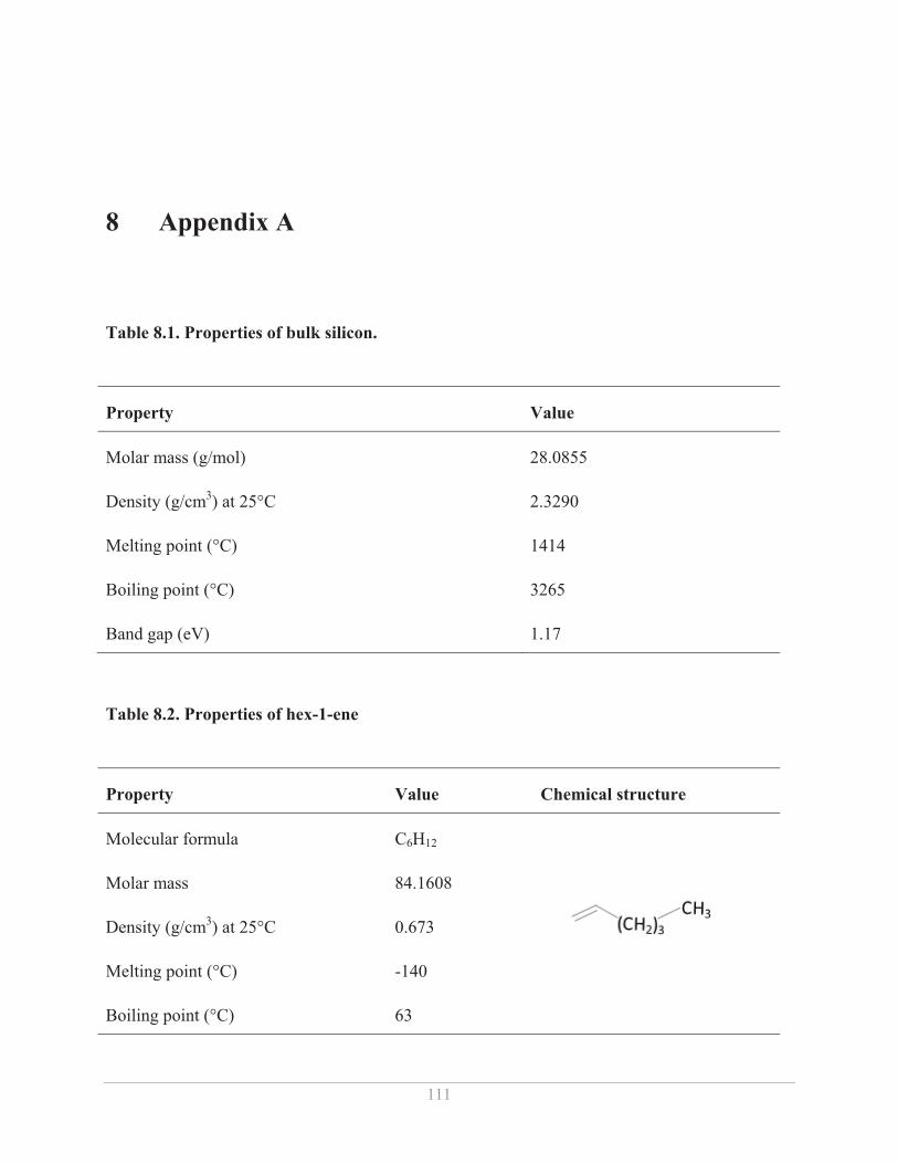
8 Appendix A
111
8 Appendix A
Table 8.1. Properties of bulk silicon.
Property Value
Molar mass (g/mol) 28.0855
Density (g/cm3) at 25°C 2.3290
Melting point (°C) 1414
Boiling point (°C) 3265
Band gap (eV) 1.17
Table 8.2. Properties of hex-1-ene
Property Value Chemical structure
Molecular formula C6H12
Molar mass 84.1608
Density (g/cm3) at 25°C 0.673
Melting point (°C) -140
Boiling point (°C) 63
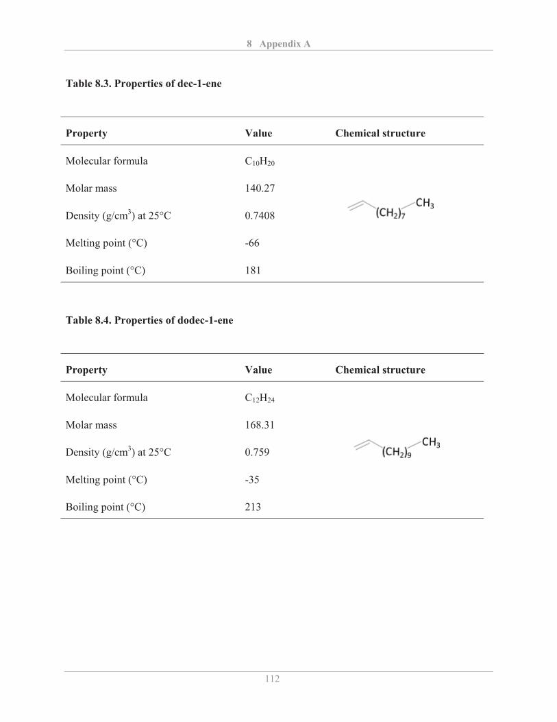
8 Appendix A
112
Table 8.3. Properties of dec-1-ene
Property Value Chemical structure
Molecular formula C10H20
Molar mass 140.27
Density (g/cm3) at 25°C 0.7408
Melting point (°C) -66
Boiling point (°C) 181
Table 8.4. Properties of dodec-1-ene
Property Value Chemical structure
Molecular formula C12H24
Molar mass 168.31
Density (g/cm3) at 25°C 0.759
Melting point (°C) -35
Boiling point (°C) 213
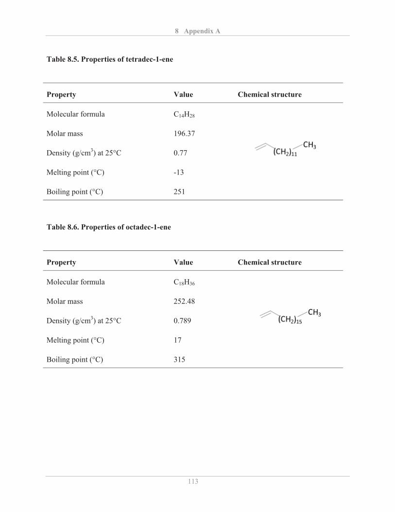
8 Appendix A
113
Table 8.5. Properties of tetradec-1-ene
Property Value Chemical structure
Molecular formula C14H28
Molar mass 196.37
Density (g/cm3) at 25°C 0.77
Melting point (°C) -13
Boiling point (°C) 251
Table 8.6. Properties of octadec-1-ene
Property Value Chemical structure
Molecular formula C18H36
Molar mass 252.48
Density (g/cm3) at 25°C 0.789
Melting point (°C) 17
Boiling point (°C) 315
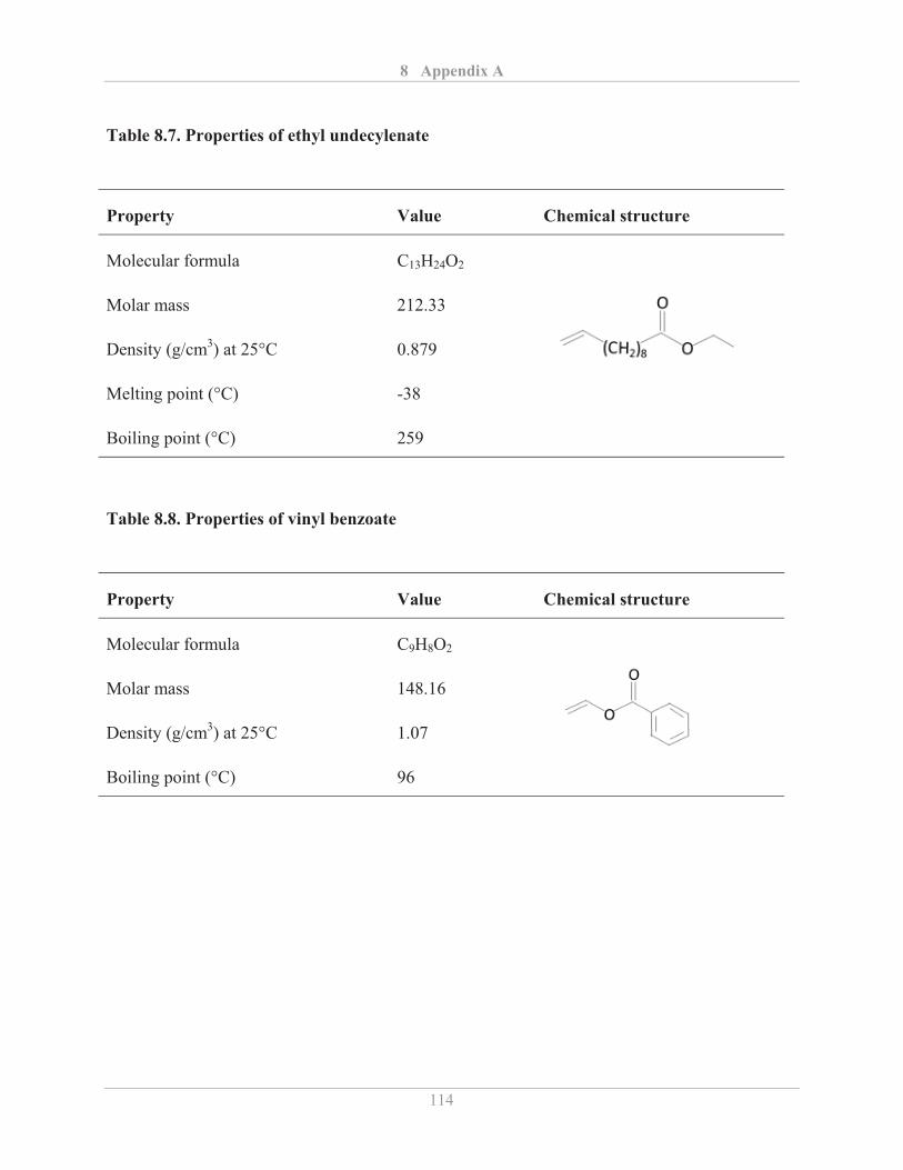
8 Appendix A
114
Table 8.7. Properties of ethyl undecylenate
Property Value Chemical structure
Molecular formula C13H24O2
Molar mass 212.33
Density (g/cm3) at 25°C 0.879
Melting point (°C) -38
Boiling point (°C) 259
Table 8.8. Properties of vinyl benzoate
Property Value Chemical structure
Molecular formula C9H8O2
Molar mass 148.16
Density (g/cm3) at 25°C 1.07
Boiling point (°C) 96
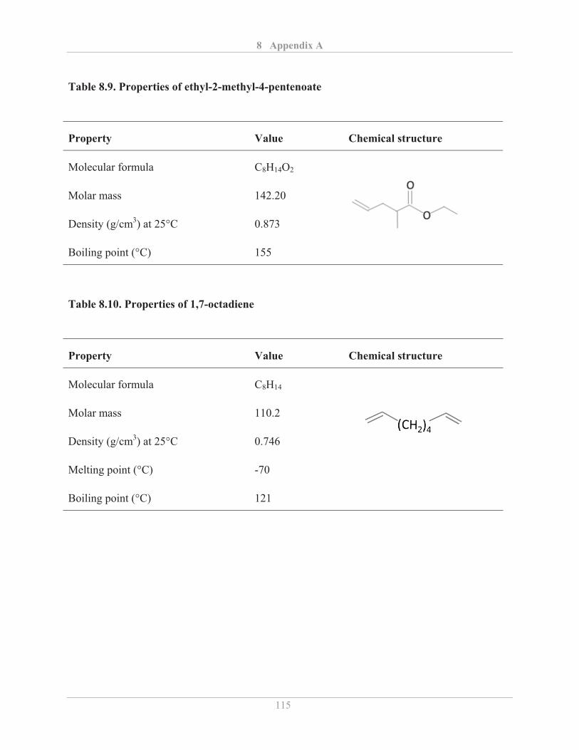
8 Appendix A
115
Table 8.9. Properties of ethyl-2-methyl-4-pentenoate
Property Value Chemical structure
Molecular formula C8H14O2
Molar mass 142.20
Density (g/cm3) at 25°C 0.873
Boiling point (°C) 155
Table 8.10. Properties of 1,7-octadiene
Property Value Chemical structure
Molecular formula C8H14
Molar mass 110.2
Density (g/cm3) at 25°C 0.746
Melting point (°C) -70
Boiling point (°C) 121
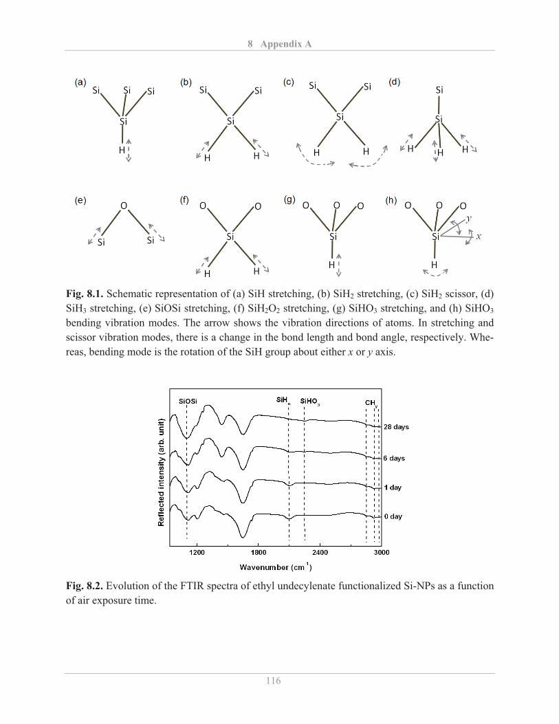
8 Appendix A
116
Fig. 8.1. Schematic representation of (a) SiH stretching, (b) SiH2 stretching, (c) SiH2 scissor, (d) SiH3 stretching, (e) SiOSi stretching, (f) SiH2O2 stretching, (g) SiHO3 stretching, and (h) SiHO3 bending vibration modes. The arrow shows the vibration directions of atoms. In stretching and scissor vibration modes, there is a change in the bond length and bond angle, respectively. Whe-reas, bending mode is the rotation of the SiH group about either x or y axis.
Fig. 8.2. Evolution of the FTIR spectra of ethyl undecylenate functionalized Si-NPs as a function of air exposure time.
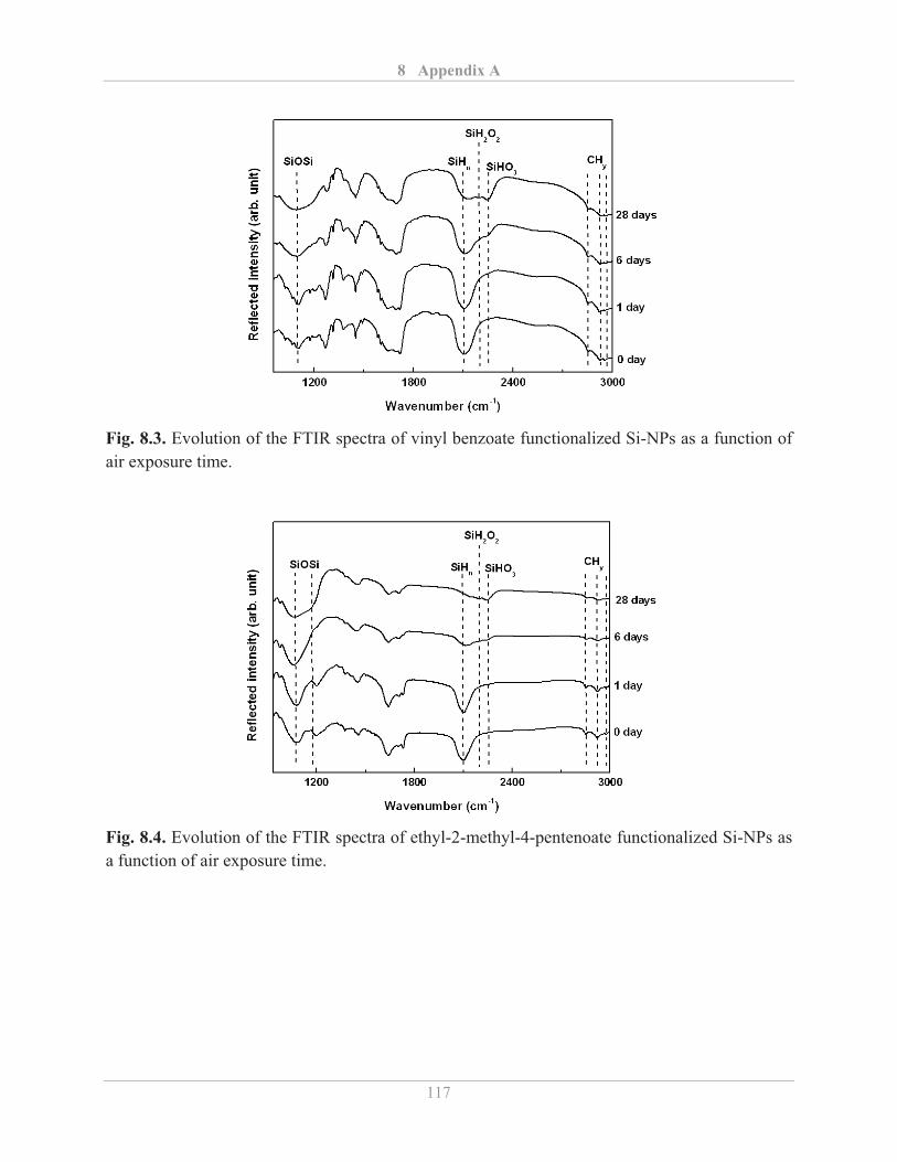
8 Appendix A
117
Fig. 8.3. Evolution of the FTIR spectra of vinyl benzoate functionalized Si-NPs as a function of air exposure time.
Fig. 8.4. Evolution of the FTIR spectra of ethyl-2-methyl-4-pentenoate functionalized Si-NPs as a function of air exposure time.
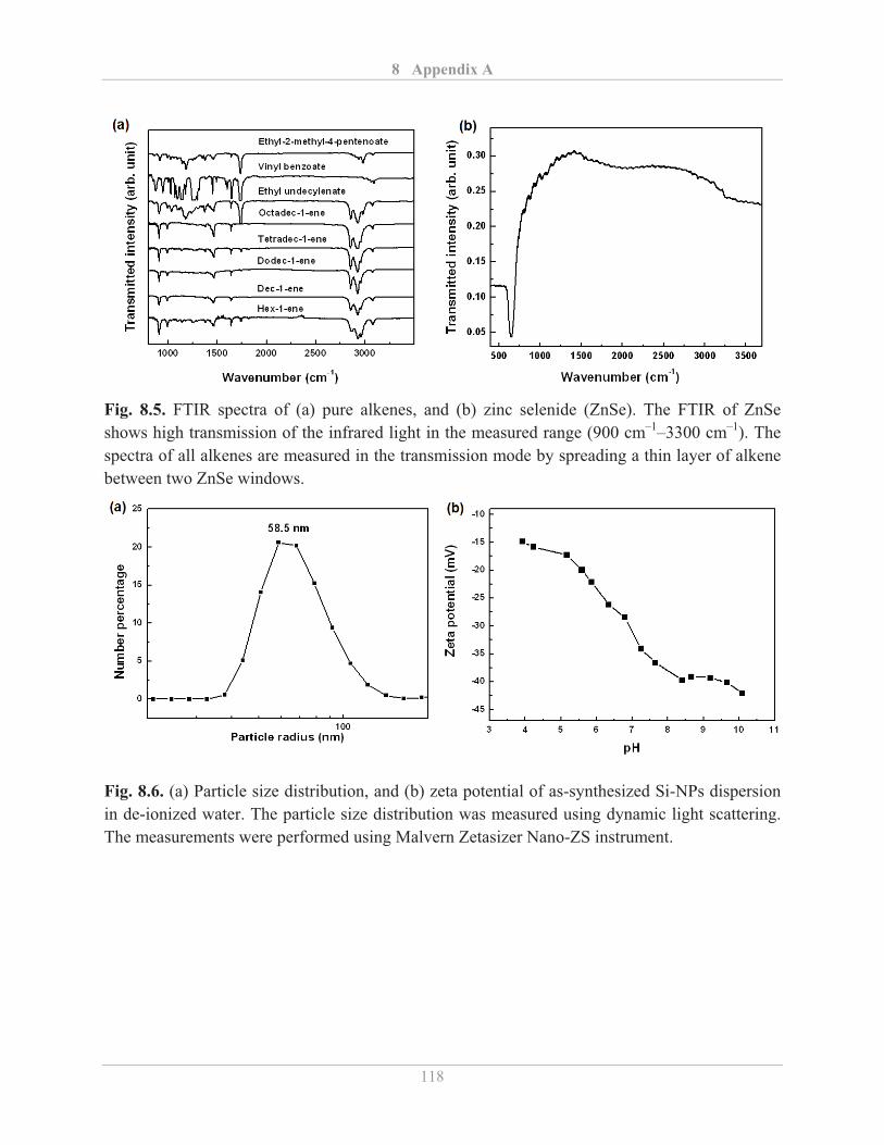
8 Appendix A
118
Fig. 8.5. FTIR spectra of (a) pure alkenes, and (b) zinc selenide (ZnSe). The FTIR of ZnSe shows high transmission of the infrared light in the measured range (900 cm–1–3300 cm–1). The spectra of all alkenes are measured in the transmission mode by spreading a thin layer of alkene between two ZnSe windows.
Fig. 8.6. (a) Particle size distribution, and (b) zeta potential of as-synthesized Si-NPs dispersion in de-ionized water. The particle size distribution was measured using dynamic light scattering. The measurements were performed using Malvern Zetasizer Nano-ZS instrument.
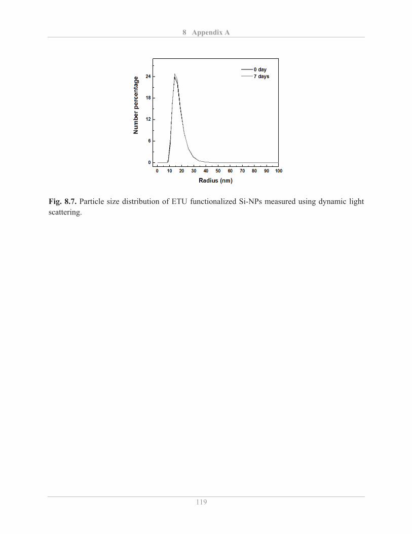
8 Appendix A
119
Fig. 8.7. Particle size distribution of ETU functionalized Si-NPs measured using dynamic light scattering.
120
List of own publications
Peer reviewed articles
1. A. Gupta, M. T. Swihart and H. Wiggers
Luminescent colloidal dispersion of silicon quantum dots from microwave plasma synthesis: Exploring the photoluminescence behavior across the visible spectrum.
Adv. Funct. Mater., 19 (2009), 696–703 (featured on cover page of the journal).
2. A. Gupta and H. Wiggers,
Surface chemistry and photoluminescence property of functionalized silicon nano-particles. Physica E, 41 (2009), 1010 – 1014.
3. A. Gupta, F. Erogbogbo, M. T. Swihart and H. Wiggers
Photoluminescence behavior of silicon nanocrystals: Role of surface chemistry and size. Mat. Res. Soc. Symp. Proc., 1145 (2009), MM10 – 04.
4. A. Gupta, A. Chuvilin, S. Mohanan, Z. Zhang, U. Kaiser and U. Herr
Investigation of the Microstructure of Co/Cu/Co/NiMn Spin Valve Systems. Sci. Adv. Mater., 1 (2009), 198 – 204.
5. A. Gupta, S. Mohanan, M. Kinyanjui, A. Chuvilin, U. Kaiser and U. Herr
Influence of nano-oxide layer on the magnetotransport properties of NiMn/Co/Cu/Co spin valve sensors. J. Appl. Phys., 107 (2010), 093910.
List of own publications
121
6. A. Gupta and H. Wiggers
Influence of etching and surface functionalization on the optical property of lumi-nescing phosphorus doped silicon nanoparticles. J. Optoelectron. Adv. Mater., 12 (2010), 518 – 522.
7. A. Gupta, S. Kluge, C. Schulz and H. Wiggers
Enhanced long-term stability of functionalized silicon nanoparticles using esters. Mat. Res. Soc. Symp. Proc., 1207 (2010), N02 – 03.
8. A. Abdali, B. Moritz, A. Gupta, H. Wiggers and C. Schulz
Hybrid microwave-plasma hot-wall reactor for synthesis of silica nanoparticles under well-controlled conditions. J. Optoelectron. Adv. Mater., 12 (2010), 440 – 444.
9. A. Gupta and H. Wiggers.
Influence of reaction parameters on the photoluminescence properties of free standing functionalized silicon nanocrystals. Mat. Res. Soc. Symp. Proc., 1260 (2010), T06 – 05.
10. A. Gupta and H. Wiggers
Freestanding silicon quantum dots: Origin of red and blue luminescence Nanotechnol., 22 (2011), 055707.
11. A. Gupta, P. Ifeacho, C. Schulz and H. Wiggers
Synthesis of tailored WO3 and WOx (2.9 < x < 3) nanoparticles by adjusting the combustion conditions in a H2/O2/Ar premixed flame reactor.
Proc. Combust. Inst., 33 (2011) 1883 – 1890.
12. A. Gupta, A.S.G. Khalil, M. Offer, M. Geller, M. Winterer, A. Lorke and H. Wig-gers
Synthesis and ink-jet printing of highly luminescing silicon nanoparticles for print-able electronics.
J. Nanosci. Nanotechnol., 11 (2011) 5028–5033.
List of own publications
122
13. A. Gupta, S. Hartner and H. Wiggers
Influence of surface chemistry on the electrical properties of silicon nanoparticles.
Submitted.
Conference articles
1. A. Gupta, C. Schulz and H. Wiggers
Optical properties of silicon nanoparticles: Influence of etching, surface oxidation and surface functionalization. Nanotech., 2 (2010), 53 – 56.
ISBN: 978-1-4398-3402-2
2. A. Gupta, A. S. G. Khalil, M. Winterer and H. Wiggers
Stable colloidal dispersion of luminescing silicon nanoparticles for ink-jet printing. Nanotech., 2 (2010), 538 – 541 .
ISBN: 978-1-4398-3402-2
3. S. Hartner, A. Gupta and H. Wiggers
Electrical properties of functionalized nanoparticles. Nanotech., 1 (2010), 376 – 378.
ISBN: 978-1-4398-3401-5
4. H. Grimm, N. Petermann, A. Gupta and H. Wiggers
Synthesis of highly-doped silicon and germanium nanoparticles in a low-pressure plasma-reactor for thermoelectric and solar applications. Nanotech., 1 (2010), 410 – 412.
ISBN: 978-1-4398-3401-5
5. A. Gupta, S. Hartner and H. Wiggers
Optical and electrical properties of silicon nanoparticles.
3rd International Nanoelectronics Conference (INEC), 2010, pp. 616 – 617.
DOI: 10.1109/INEC.2010.5424734
List of own publications
123
6. A. Gupta, A. S. G. Khalil, M. Winterer and H. Wiggers
Stable colloidal dispersions of silicon nanoparticles for the fabrication of films using inkjet printing technolog. 3rd International Nanoelectronics Conference (INEC), 2010, pp. 1018 – 1019.
DOI: 10.1109/INEC.2010.5425068
7. A. S. G. Khalil, S. Hartner; M. Ali, A. Gupta, H. Wiggers and M. Winterer
Stable aqueous dispersions of ZnO nanoparticles for ink-jet printed gas sensors.
3rd International Nanoelectronics Conference (INEC), 2010, pp. 440 – 441.
DOI: 10.1109/INEC.2010.5424503

124