Embed Size (px)
Citation preview

Tao Hong
Transient Avalanche Oscillation of IGBTs Under High Current

Tao Hong
Transient Avalanche Oscillation of IGBTs
Under High Current
Universitätsverlag Chemnitz
2015
Impressum
Bibliograsche Information der Deutschen Nationalbibliothek
Die Deutsche Nationalbibliothek verzeichnet diese Publikation in der Deut-schen Nationalbibliograe; detaillierte bibliograsche Angaben sind im In-ternet über http://dnb.d-nb.de abrufbar.
Technische Universität Chemnitz/UniversitätsbibliothekUniversitätsverlag Chemnitz
09107 Chemnitzhttp://www.tu-chemnitz.de/ub/univerlag
Herstellung und Auslieferung
Verlagshaus Monsenstein und Vannerdat OHGAm Hawerkamp 3148155 Münsterhttp://www.mv-verlag.de
ISBN 978-3-944640-52-5
http://nbn-resolving.de/urn:nbn:de:bsz:ch1-qucosa-164238
Transient Avalanche Oscillation
of IGBTs Under High Current
Doctoral Thesis
to obtain the academic degree of
Doctor of engineering (Dr.-Ing.)
submitted to
Faculty of Electrical Engineering and Information Technology
at Chemnitz University of Technology
by Diplom-Ingenieur Tao Hong
born on 1971/07/09 in Hebei China
Date of submission: 14/10/2014
Date of the defence: 11/03/2015
Examiner: Prof. Dr.-Ing. Josef Lutz
Co-examiner: Prof. Dr. phil. nat. D. Silber

Acknowledgements
This work was conducted during my Ph.D contract with Inneon Tech-
nologies AG and as employee of the team called Innovative Concepts. I
thank Inneon for the opportunity to investigate the oscillations of IGBT
Modules and the provision of laboratory conditions.
I would like to take this opportunity to thank Dr. Reinhold Bayerer.
His wide overview of power modules has led me to the work eld on high
frequency oscillations in IGBTs. The fruitful technical discussion with him
and his technical and organizational support made this work possible.
I would like to express my special thanks to Dr. Frank Prsch. His
provision of basic structure of an IGBT cell facilitated my training in the
device simulation. Through our discussions, I received numerous benets
from his professional experience on power semiconductors in tting the
IGBT device model regarding the forward and blocking characteristics.
I would like to express my gratitude to my supervisor Prof. Dr. Josef
Lutz. He provides me the device simulation tools which are necessary for
the analysis on the HF-oscillation. His extensive expertise has relieved me
from the search the state of the art. And I thank him for his great patience
in the proofreading my thesis.
I would like to express my great appreciation to my second supervisor
Prof. Dr. phil. nat. Dieter Silber, for the valuable technical discussions on
space charge limited current ow and valuable information on the interac-
tion of IMPATT and PETT.
I would like to thank Mrs. Susanne Fichtner and Dr. Thomas Basler, for
their indispensable support during the incorporation of Sentaurus Device
Simulator and in the ongoing maintenance of my simulation computer at
the Chemnitz University of Technology. The material parameter set of
silicon from Dr. Thomas Basler has saved me a lot of detours and time.
I wish to acknowledge the assistance on the familiarization in the 3.3

kV IGBT oscillations provided by Mr. Thomas Gutt, Dr. Maria Cotorogea,
Mr. Ronny Herms, Mr. Daniel Heer and Mr. Karl-Heinz Hoppe. And I also
thank Dr. Markus Thoben for the methodical discussions.
Ms. Karin Schulze deserves my thanks for her assistance in both the
patent registration and proofreading the German abstract of my thesis. I
thank Dr. Han Hong, Mr. Rashedul Karim and Mr. William Etienne Akem
for the proofreading English part this thesis.
Also, I thank all colleagues during my work at Inneon for their kind
encouragement.
I wish to thank my parents and my brothers for their encouragements
and cares in my life. Finally, I am immensely grateful for the essential
support of my wife Hui Juan and the smiles of my Kids.
Contents
Zusammenfassung 1
Abstract 2
1 Introduction 3
2 Functionality, turn-o and phenomenons of RF-oscillations
in IGBT modules 7
2.1 Functionality of modern IGBTs . . . . . . . . . . . . . . . 8
2.2 Basic design of IGBT modules . . . . . . . . . . . . . . . . 9
2.3 IGBT turn-o . . . . . . . . . . . . . . . . . . . . . . . . . . 11
2.4 Possible RF-oscillations during IGBT switching . . . . . . . 21
2.4.1 Tail oscillation PETT . . . . . . . . . . . . . . . . . 21
2.4.2 Dynamic IMPATT oscillation . . . . . . . . . . . . . 25
2.4.3 Transient Avalanche oscillations . . . . . . . . . . . . 29
3 Mechanisms of Transit time eect and RF-oscillations in
IGBT Modules 31
3.1 Amplication process . . . . . . . . . . . . . . . . . . . . . . 32
3.1.1 Avalanche breakdown . . . . . . . . . . . . . . . . . 33
3.1.2 Amplication eciency . . . . . . . . . . . . . . . . 35
3.2 Resonant circuits in IGBT modules . . . . . . . . . . . . . . 40
i
4 Analysis of Transient Avalanche oscillation 41
4.1 Measurement of TA-oscillations . . . . . . . . . . . . . . . . 42
4.1.1 TA-oscillation on IGBT modules . . . . . . . . . . . 42
4.1.2 TA-oscillation on a substrate and single chip . . . . 48
4.2 Analysis of the resonant circuits . . . . . . . . . . . . . . . . 59
4.2.1 Inductance of wire bonds . . . . . . . . . . . . . . . 60
4.2.2 Dierential capacitance of IGBTs and diodes . . . . 63
4.3 Device simulations . . . . . . . . . . . . . . . . . . . . . . . 65
4.3.1 Circuit . . . . . . . . . . . . . . . . . . . . . . . . . . 67
4.3.2 Eect of resonant circuit's eigenfrequencies . . . . . 68
4.3.3 Eect of load current . . . . . . . . . . . . . . . . . . 71
4.3.4 Eect of gate resistance . . . . . . . . . . . . . . . . 74
4.3.5 Internal process of IGBT chips . . . . . . . . . . . . 75
4.3.6 Eect of impact ionization . . . . . . . . . . . . . . . 76
4.4 Summarized explanation of TA-oscillations . . . . . . . . . 80
5 Countermeasures to Transient Avalanche oscillations 83
5.1 Essential measures
to suppress TA-oscillations . . . . . . . . . . . . . . . . . . . 83
5.2 Driver concept to suppress TA-oscillations - pace maker . . 85
6 Summary and outlook 91
6.1 Summary . . . . . . . . . . . . . . . . . . . . . . . . . . . . 91
6.2 Outlook . . . . . . . . . . . . . . . . . . . . . . . . . . . . . 94
A Derivation of transit time eciency 97
B Test box and the RF-noise problems 101
Bibliography 103
ii
List of symbols
αeff eective ionization coecient 1/cm
αn,p ionization coecient of electrons, holes 1/cm
ϵ relative permittivity −
ϵ0 vacuum permittivity As/V m
η eciency coecient of the RF-power conversion −
η1 injection dependent eciency coecient −
η2 transit time dependent eciency coecient −
λ proportionality between Nh_nett and ICE −
υdn,dp eective velocity of electrons, holes cm/s
ΘD transit angle −
ΘM phase angle of the injection −
ΘW injection angle −
υdn,dp drift velocity of electrons, holes cm/s
υQ velocity of charge carrier cm/s
iii
A chip area cm2
CDC DC-link capacitor F
Cdiff eective capacitance in RF-range F
CDiode dierential capacitance of SCR in diode F
CIGBT dierential capacitance of SCR in IGBT F
EC critical E-eld strength V/cm
Emax maximal E-eld in the space charge region V/cm
I current A
IL load current, trun-o current of IGBT A
IN norm current A
Iwb load current in the wire bonds A
JDC induced average current density A/cm2
Jind induced current density on the terminal A/cm2
l coil length mm
La inductance of the avalanche region H
LB1,B2 inductance of wire bonding H
Llc,sc inductance of long, short coil H
LP load inductance H
Lwb inductance of wire bondings H
NA density of the acceptors 1/cm3
ND density of donors 1/cm3
iv
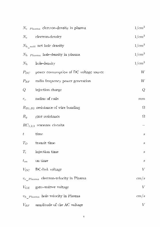
Ne_Plasma electron-density in plasma 1/cm3
Ne electron-density 1/cm3
Nh_nett net hole-density 1/cm3
Nh_Plasma hole-density in plasma 1/cm3
Nh hole-density 1/cm3
PDC power consumption of DC voltage source W
PRF radio frequency power generation W
Q injection charge Q
rc radius of coils mm
RB1,B2 resistance of wire bonding Ω
Rg gate resistance Ω
RC1,2,3 resonant circuits −
t time s
TD transit time s
Ti injection time s
ton on time s
VDC DC-link voltage V
ve_Plasma electron-velocity in Plasma cm/s
VGE gate-emitter voltage V
vh_Plasma hole-velocity in Plasma cm/s
VRF amplitude of the AC voltage V
v

VT terminal voltage on the transit time structure V
WA width of the avalanche region cm
Wc eld energy of coils W
WSCR width of the space charge area cm
Wwb eld energy of emitter wire bondings W
vi
Zusammenfassung
Radio Frequenz Oszillationen bis zu mehreren hundert MHz wurden wäh-
rend des Abschaltens von Hochstrom leitenden IGBTs beobachtet. Sie wer-
den in dieser Arbeit als Transient Avalanche Oscillationen beschrieben.
Anders als PETT Oszillationen, die in der Tail-Strom Phase vorkommen,
erscheint diese Oszillation während des Anstiegs der Kollektor-Emitter-
Spannung VCE und des Fallens des Kollektor-Emitter Stroms ICE . In die-
ser Arbeit werden die Abschaltvorgänge von IGBTs mit Hilfe von Messun-
gen, Schaltungs- bzw. Device-Simulationen untersucht, um die Wirkungs-
mechanismen der transient erscheinenden hochfrequenten Oszillationen zu
erklären. Es ist erstmals gelungen solche Transient Avalanche Oszillationen
mit der Simulation zu reproduzieren und anschlieÿend die Einüsse einzel-
ner Parameter zu untersuchen. Die Beteiligung des IMPATT Mechanismus
an der Transient Avalanche Oszillation wurde nachgewiesen. Die Interak-
tion von IMPATT und PETT während Aufbau der Raumladungszone im
IGBT wurde untersucht. Maÿnahmen zur Unterdrückung der Oszillation
werden auf den Ebenen von Chip-Design, Modulauslegung und der Trei-
berschaltung diskutiert. Das Zuführen des Elektrostromes während der
kritischen Phase wird als ein eective Methode zur Vermeidung der TA-
Oscillation nachgewiesen.
IGBT, Abschalten, Oszillation, Transient Avalanche, Resonanz, Raum-
ladung, IMPATT, PETT, TA-Oszillation
1
Abstract
Radio frequency oscillations up to several hundreds of MHz were observed
during turn-o the high-current conducting IGBTs. They are described in
this work as Transient Avalanche oscillations. Other than PETT oscilla-
tions that happen in the tail current phase, this oscillation appears during
the rise of collector-emitter voltage VCE and during the fall of the collector-
emitter current ICE . The turn-o process of IGBTs are investigated with
the help of measurements, the circuit- and device-simulations to reveal
the working mechanisms of transient high-frequency oscillations. For the
rst time the Transient Avalanche Oscillation is successfully reproduced
with computer simulation, which allows the further investigation on the
inuences of individual parameters. The participation of IMPATT mech-
anism in Transient Avalanche oscillation is demonstrated. The interaction
between IMPATT mechanism und PETT mechanism during the setting
up of depletion region in IGBTs was investigated. Measures to suppress
such oscillation are discussed on the levels of chip design, module design
and the driver concept. Supplying electron current during critical phase is
found to be an eective method to avoid the dynamic avalanche and the
TA-oscillation.
IGBT, turn-o, Oscillation, Transient Avalanche, Resonance, Space
charge, depletion region, IMPATT, PETT, TA-oscillation
2
Chapter 1
Introduction
In addition to the reliability, higher blocking capability, lower conduction
losses, lower switching losses and higher switching frequency are the basic
requirements for designing power semiconductors. The approach to im-
prove such properties by combining the advantages of MOSFET (metal-
oxide-semiconductor eld-eect transistor) and BJT (bipolar transistor)
was reported in the late seventies [Bal79]. In 1980 the U.S. Patent Of-
ce granted a U.S. patent Power MOSFET with an anode region with
patent No. 4,364,073 to Hans W. Becke and C. Frank Jr. Wheathley
[BW80]. This patent is regarded as the invention of the insulated gate
bipolar transistor, briey called IGBT, which merged BJT and MOSFET
technically.
After the development over three decades, more and more approaches
have been developed by advantageous combination of bipolar and unipolar
elements. Up to date, IGBT nds wider and wider application elds.
Parallel to the industrial motor control and inverters of renewable energy,
IGBTs are also widely used in traction applications, auto mobiles and
consumer electronics. The application area of IGBTs extends even to the
typical application area of thyristors with the development of high power
4 CHAPTER 1. INTRODUCTION
IGBTs. The rst 3.3kV IGBT Module was developed by Eupec GmbH in
1995. The rst 6.5kV IGBT module was developed also by Eupec GmbH
in 1999 [ABG+99]. The development of 8kV IGBT and diode chips was
reported in 2002 [RKK+02]. Up to date the 6.5kV IGBT modules are still
the commercially available Modules with maximal blocking capability.
One important aspect of the IGBT development focuses on the reduc-
tion of conduction and switching losses and to increase the current density
on silicon. To full increasing demands on the electrical and thermal per-
formance in high power applications, IGBTs and diodes are paralleled and
integrated in modules. In the modules, IGBT chips work in a complicated
parasitic environment which consists of IGBT capacitance, diode capac-
itance, parasitic inductances and capacitances as a consequence of the
module construction. Such parasitic components build up resonant cir-
cuits. In the dynamic process, such as turn-on and turn-o, the resonant
circuits can be excited which cause undesirable oscillations. Especially the
high-frequency oscillations can cause electromagnetic interference for the
complete system.
Under a special design of a module, high frequency oscillations of up to
several hundreds of megahertz are observed during turn-o of the IGBT.
This oscillation phenomena has been found in the tail current phase of
NPT IGBTs in at package [TYK+97] and was explained by the the
mechanism of plasma extraction transit time (PETT) oscillation [GMS01]
[GMS02] [SLNM03]. The PETT oscillations were usually observed during
the tail current. After the IGBT has taken the reverse voltage, there is
still electron-hole plasma remaining close to the collector side. This resid-
ual plasma is extracted out of IGBT by the tail current. The holes drift
through space charge region (SCR) under the inuence of the strong elec-
tric eld to the emitter side and recombine with electrons. The holes need
a certain time to be injected in to the space charge region and a transit
time to drift through the space charge zone. Such injection time and the
5
transit time together induce a phase shift between terminal voltage and the
terminal current in the RF-frequency range. For a certain frequency range
the phase shift lies in the interval between 1π/2 and 3π/2. The generates
therefore power and works in this frequency range as an amplier. This
BARITT-diode similar mechanisms (barrier injection transit-time diode)
[Roe77] [Sze81] was analysed in details in [Gut06] and [SMNL06]. RF-
frequency oscillations has also been found during the turn-o of fast re-
covery diode. The temporarily charged K-defects, radiation induced deep
levels, leads to the temporary reduction of the avalanche breakdown volt-
age and lead to the dynamic IMPATT (Impact Ionization Avalanche Tran-
sit Time) oscillation during diode turn-o [LSG98] [Lut00] [SLH04]. Both
IMPATT and PETT oscillations lead to deterioration of EMC and should
be avoided. consequently [SLNM03].
Recently a new type of high-frequency oscillation was found during the
turn-o of IGBTs. It happens in the dynamic avalanche [SN89] [DLS03]
phase during the rise of the collector-emitter voltage and the fall of the
collector-emitter current. At the moment of oscillation, the load current or
a large portion of the load current is still owing. Since this oscillation is
observed only transiently and only during the dynamic avalanche process,
it is called Transient Avalanche oscillation (TA-oscillation) [HPB+14].
The mechanisms of this oscillation seems to be closely related to the pro-
cess found in IMPATT diode [EH98]. The target of this work is to reveal its
mechanism and to gure out the countermeasures to prevent or suppress
such TA-oscillations.
In Chapter 2, the construction and characterizations of IGBTs are
shown. The IGBT turn-o process is described according to the inter-
nal semiconductor states. Finally, the state of art mechanisms of PETT
oscillation and the dynamic IMPATT oscillation is represented.
In Chapter 3, the theoretical analysis for the transit-time eect and
mechanisms of IMPATT- and BARITT-diode are summarized. The anal-
6 CHAPTER 1. INTRODUCTION
ysis of the eciency of the transit-time eect in the space charge zone of
the IGBTs results in the basic of theoretical explanation of the TA oscil-
lation. Whereas eciency means the eciency to amplify RF-oscillations
by the TA-eect.
The detailed investigation of the TA-oscillation by means of measure-
ments, resonant circuit analysis and simulations are presented and followed
by the theory of the TA-oscillation in Chapter 4.
In chapter 5, the countermeasures of TA-oscillation are investigated,
and a new driver concept is introduced to suppress TA-oscillation.
The summary in chapter 6 provides an overview of the HF-frequency
oscillations in power modules, that is followed by the outlook on the further
possibilities to suppress such oscillation by methods of module design and
chip designs.
Chapter 2
Functionality, turn-o and
phenomenons of
RF-oscillations in IGBT
modules
To analyse the TA-oscillation mentioned in Chapter 1, it is necessary to
understand the functionality of IGBT and to describe the turn-o process
with the internal semiconductor states. A hypothesis on the mechanisms
of TA-oscillation can be set up based on the results of the investigation on
the relationships between IGBT-, diode-chips and parasitic components of
the IGBT modules constructions.
8 CHAPTER 2. IGBT
n+
p
n+
p-float
n base-
p+
n+
pnp
Tra
nsi
stor
npn M
OS
emitter (cathode metallziation)
Gate oxideGate-Poly-Si
collector (anode metallization)
J1
J2
-E
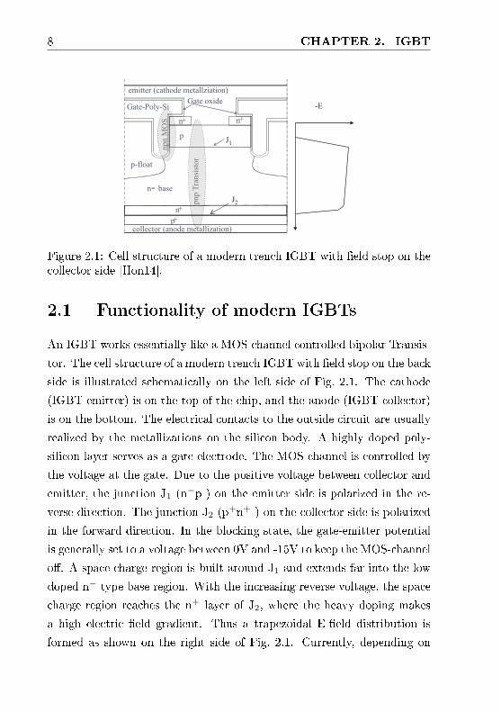
Figure 2.1: Cell structure of a modern trench IGBT with eld stop on thecollector side [Hon14].
2.1 Functionality of modern IGBTs
An IGBT works essentially like a MOS-channel controlled bipolar Transis-
tor. The cell structure of a modern trench IGBT with eld stop on the back
side is illustrated schematically on the left side of Fig. 2.1. The cathode
(IGBT emitter) is on the top of the chip, and the anode (IGBT collector)
is on the bottom. The electrical contacts to the outside circuit are usually
realized by the metallizations on the silicon body. A highly doped poly-
silicon layer serves as a gate electrode. The MOS-channel is controlled by
the voltage at the gate. Due to the positive voltage between collector and
emitter, the junction J1 (n−p ) on the emitter side is polarized in the re-
verse direction. The junction J2 (p+n+ ) on the collector side is polarized
in the forward direction. In the blocking state, the gate-emitter potential
is generally set to a voltage between 0V and -15V to keep the MOS-channel
o. A space charge region is built around J1 and extends far into the low
doped n− type base region. With the increasing reverse voltage, the space
charge region reaches the n+ layer of J2, where the heavy doping makes
a high electric eld gradient. Thus a trapezoidal E-eld distribution is
formed as shown on the right side of Fig. 2.1. Currently, depending on
2.2. BASIC DESIGN OF IGBT MODULES 9
the thickness of the base region IGBTs can be commercially designed for
a blocking capability up to 6.5 kV.
In forward operation, the gate-emitter voltage is usually switched to
+15V. The MOS-channel is turned on. Electrons ow through the MOS
channel and n− base region to junction J2 on the collector side. Similar to
a bipolar transistor, holes from p+ are injected into the n− base. Due to
the wide n− base of the PNP-transistor (see Fig. 2.1), the current gain of
the transistor is less than one [Sil05]. That is, its base current is greater
than the collector current. As the PNP transistor gets into the on-state,
holes get from the p+ layer (collector) in the n− base. The base is than
ooded with an electron-holes plasma und gets in the state of high in-
jection. This results in a good conductivity in the forward operation of
the IGBT. The hole current ow is suppressed by the deep trench gate
geometry. The injection eciency of holes near to J1 at the emitter side
is therefore enhanced. A plasma distribution similar to a thyristor can
be realized due to this injection enhancement eect [KOH+93] [OOSO97].
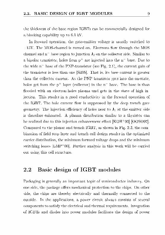
Compared to the planar and trench IGBT, as shown in Fig. 2.2, the com-
bination of eld stop layer and trench cell design results in the optimized
carrier distribution, the minimum forward voltage drops and the minimum
switching losses [LMP+00]. Further analysis in this work will be carried
out using this cell structure.
2.2 Basic design of IGBT modules
Packaging is generally an important topic of semiconductor industry. On
one side, the package oers mechanical protection to the chips. On other
side, the chips are thereby electrically and thermally connected to the
outside. In the applications, a power circuit always consists of several
components to satisfy the electrical and thermal requirements. Integration
of IGBTs and diodes into power modules facilitate the design of power
10 CHAPTER 2. IGBT
Figure 2.2: Plasma distributions of Planar-IGBT, Trench-IGBT andTrench FS-IGBT [LMP+00] [R.B10]
electronics.
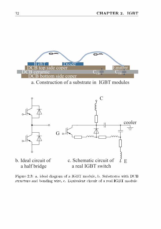
DCB-substrates (direct copper bounding) are frequently used as the
circuit substrate in the IGBT modules where two copper layers are bonded
on each side of a ceramic sheet. Fig. 2.3a. shows the construction of such
a substrate equipped with IGBT and diode chips. IGBT- and diode-chips
are bonded on the top side of a DCB. The top side copper layer of the DCB
serves as the circuit carrier. The ceramic and the bottom copper layer of
the DCB ensure the electrical insulation and heat conduction to the heat
sink. Wire-bonds are applied to realize the electrical connection between
the top side of the chips and electrical terminals on the DCB. Fig. 2.3b.
shows an half bridge circuit. The circuit consists of two IGBTs connected
in series and their anti-parallel free-wheeling diodes.
Besides the desired electrical and thermal connections, the module
structure results in inevitable parasitic eects. The parasitic electrical re-
sistances and inductances of the bond wires, parasitic capacitance within
2.3. IGBT TURN-OFF 11
the substrate are some main parasitic components of a module structure.
The equivalent circuit of an IGBT module, as can be seen in Fig. 2.3c, is
therefore much more complex than the circuit in Fig. 2.3b. The circuits
for parallel connected dies are even more complex than Fig. 2.3c. The par-
asitics of the module structure together with the semiconductor chips may
constitute resonant circuits which are excited during switching processes
resulting in oscillations. This leads to signicant deviation from the ideal
clean switching [BD10]. The switching performances is worthened by such
oscillations. Further investigation of the resonant circuit will be addressed
in Chap.4.2.
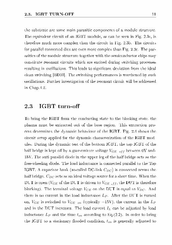
2.3 IGBT turn-o
To bring the IGBT from the conducting state to the blocking state, the
plasma must be extracted out of the base region. This extraction pro-
cess determines the dynamic behaviour of the IGBT. Fig. 2.4 shows the
circuit setup applied for the dynamic characterization of the IGBT mod-
ules. During the dynamic test of the bottom IGBT, the top IGBT of the
half bridge is kept o by a gate-emitter voltage VGE_off between 0V and-
15V. The anti-parallel diode in the upper leg of the half bridge acts as the
free-wheeling diode. The load inductance is connected parallel to the Top
IGBT. A capacitor bank (so-called DC-link CDC) is connected across the
half bridge. CDC acts as an ideal voltage source for a short time. When the
DUT is open (VGE of the DUT is driven to VGE off , the DUT is therefore
blocking). The terminal voltage VCE on the DUT is equal to VDC . And
there is no current in the load inductance LP . After the DUT is turned
on, VGE is switched to VGE_on (typically +15V), the current in the LP
and in the DUT increases. The load current IL can be adjusted by load
inductance LP and the time ton according to Eq.(2.2). In order to bring
the IGBT to a stationary ooded condition, ton is generally adjusted to
12 CHAPTER 2. IGBT
b. Ideal circuit ofa half bridge
a. Construction of a substrate in IGBT modules
c. Schematic circuit ofa real IGBT switch
C
G
E
cooler
IGBTDCB top side coper Emitter
Diode
DCB bottom side coperCCB
CEB
CD
DCB ceramic
Figure 2.3: a. ideal diagram of a IGBT module, b. Substrates with DCBstructure and bonding wire, c. Equivalent circuit of a real IGBT module
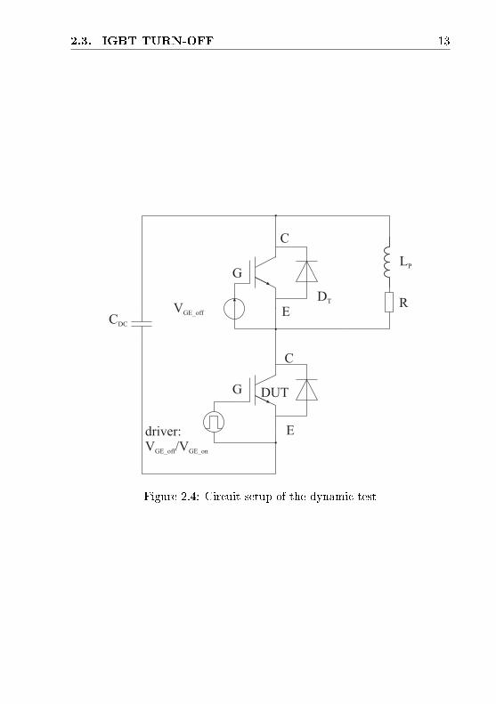
2.3. IGBT TURN-OFF 13
VGE_off
CDC
LP
G
C
E
DT
DUT
driver:V /VGE_off GE_on
G
C
ER
Figure 2.4: Circuit setup of the dynamic test
14 CHAPTER 2. IGBT
more than 100µs.
dILdt
=VDC
LP(2.1)
IL = tonVDC
LP(2.2)
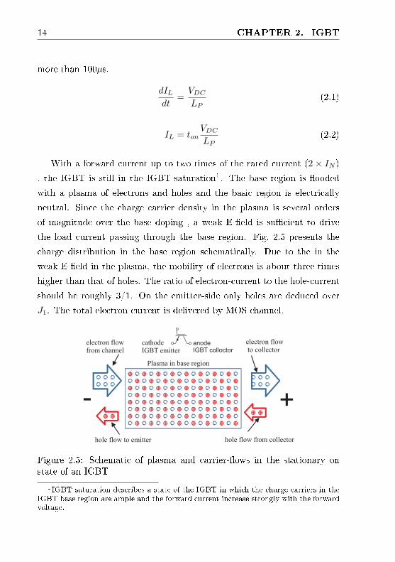
With a forward current up to two times of the rated current (2 × IN )
, the IGBT is still in the IGBT-saturation1. The base region is ooded
with a plasma of electrons and holes and the basic region is electrically
neutral. Since the charge carrier density in the plasma is several orders
of magnitude over the base doping , a weak E-eld is sucient to drive
the load current passing through the base region. Fig. 2.5 presents the
charge distribution in the base region schematically. Due to the in the
weak E-eld in the plasma, the mobility of electrons is about three times
higher than that of holes. The ratio of electron-current to the hole-current
should be roughly 3/1. On the emitter-side only holes are deduced over
J1. The total electron-current is delivered by MOS channel.
-
-
-
-
-
-
-
-
-
-
-
-
-
-
-
-
-
-
-
-
-
-
-
-
-
-
-
-
-
-
-
-
-
-
-
-
-
-
-
-
-
-
-
-
-
-
-
-
-
-
-
-
-
-
-
-
-
-
-
-
-
-
-
-
-- -
- --
-- -
- --
hole flow to emitter hole flow from collector
electron flowfrom channel
electron flowto collector
Plasma in base region
- +
cathodeIGBT emitter
anode
IGBT colloctor
Figure 2.5: Schematic of plasma and carrier-ows in the stationary onstate of an IGBT
1IGBT-saturation describes a state of the IGBT in which the charge carriers in the
IGBT base region are ample and the forward current increase strongly with the forward
voltage.
2.3. IGBT TURN-OFF 15
Time (µs)
0 1 2 3 4
V(V
)G
E
0
10
20
V(V
), I
(A)
CE
GE
0
1000
2000
3000
t0
t2
t7
t3
t4
t5
t6
t1
ICE
VGE
VCE
Figure 2.6: Turn-o diagram of a 3.3kV Trench Field Stop IGBT (simula-tion)
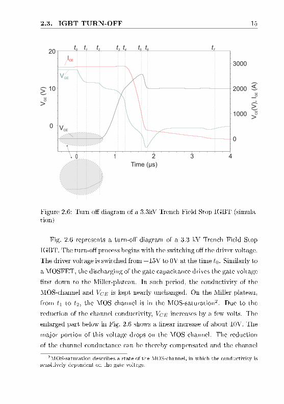
Fig. 2.6 represents a turn-o diagram of a 3.3 kV Trench Field Stop
IGBT. The turn-o process begins with the switching o the driver voltage.
The driver voltage is switched from +15V to 0V at the time t0. Similarly to
a MOSFET, the discharging of the gate capacitance drives the gate voltage
rst down to the Miller-plateau. In such period, the conductivity of the
MOS-channel and VCE is kept nearly unchanged. On the Miller plateau,
from t1 to t2, the MOS channel is in the MOS-saturation2. Due to the
reduction of the channel conductivity, VCE increases by a few volts. The
enlarged part below in Fig. 2.6 shows a linear increase of about 10V. The
major portion of this voltage drops on the MOS channel. The reduction
of the channel conductance can be thereby compensated and the channel
2MOS-saturation describes a state of the MOS-channel, in which the conductivity is
sensitively dependent on the gate voltage.
16 CHAPTER 2. IGBT
current is maintained. Because of the Miller capacitance, the feedback
of VCE on the gate is so strong that the VGE remains almost constant
in this period. Such behaviour can also be found on the Miller-plateau
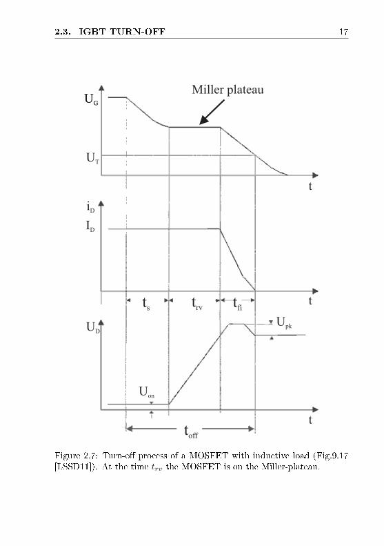
during turn-o of a MOSFET (Fig. 2.7). The channel current vanished
with further discharging the gate capacity.
From time t2, the IGBT passes to the active-state3. The channel cur-
rent begins to decrease with the gate voltage. The sinking of channel
current means less incoming electrons from the emitter side to the base
region. Because VCE is still below the VDC , the load current can not be
commutated to the free-wheeling diode. The total load current must be
carried by the IGBT. On the emitter side the missing electron-current
must be taken over by holes. The electrical neutrality under the J1 is
broken. A layer of space charge with a net holes density of Nh_net ap-
pears in the vicinity of J1. The space charge region SCR is formed and
expands with the time to the collector. Poisson-equation (2.3) describes
the dependence between the electric eld and charge density in the SCR.
Since the charge carrier density is much higher than the base doping, in
one dimensional-case Eq.(2.3) can be expressed to Eq.(2.4).
∂E
∂x=
q
ϵϵ0(ND −NA +Nh −Ne) (2.3)
with Nh_net = Nh −Ne ≫ ND −NA
dE
dx=
q
ϵϵ0Nh_net (2.4)
With the modern computer technology, the essential semiconductor equa-
tions can be numerically solved by the Device Simulators to represent the
3In the active-state of a IGBT, the channel current is linearly dependent on the gate
voltage.
2.3. IGBT TURN-OFF 17
Miller plateauUG
ts trv
toff
UG
Upk
UT
ID
iD
UD
Uon
t
t
t
tfi
Figure 2.7: Turn-o process of a MOSFET with inductive load (Fig.9.17[LSSD11]). At the time trv the MOSFET is on the Miller-plateau.
18 CHAPTER 2. IGBT
dynamic processes in semiconductors. Nevertheless the following analyti-
cal assessment is often useful to better understand the processes.
During the turning-o of IGBTs, the building-up of SCR can be ana-
lytically derived under the following assumptions and simplications ap-
proximately.
Homogeneous charge distribution and neutrality in the plasma with
the charge density NPlasma = Nh_Plasma = Ne_Plasma
Homogeneous charge distribution and triangular E-eld distribution
in main part of SCR
In the plasma the electron velocity ve_Plasma is three times higher
than that of the holes vh_Plasma.
ICE = AqNPlasma
(vh_Plasma + ve_Plasma
)(2.5)
A: chip area
With ve_Plasma = 3vh_Plasma the velocity of the electrons in the plasma
can be represented as a function of load current and plasma density. The
SCR extends to the collector with the velocity ve_Plasma. After the turn-
o of the channel current the neutral plasma front drifts toward the collec-
tor with the velocity of ve_Plasma. For the same IGBT, higher load current
would lead to higher electron velocity in the plasma during the on-state
and therefore leads to the faster extension of SCR during turning-o.
ve_Plasma =3
4
ICE
AqNPlasma(2.6)
WSCR = ve_Plasma (t− t2) (2.7)
The space charge, QSCR in Eq.(2.8) and the maximum eld strength, Emax
2.3. IGBT TURN-OFF 19
in Eq.(2.10), increases rst linearly withWSCR. Accordingly, the collector-
emitter voltage VCE increases proportionally to the square of WSCR. In
the analysis of high-frequency oscillations, the instantaneous chip capacitor
of SCR and it's eect of the resonant circuit are important factors. A
dierential capacitance Cdiff can be dened as Eq.(2.9). Cdiff acts as the
instantaneous chip capacitor. It is inversely proportional to WSCR. This
can also be applied to the reverse-biased diodes. Generally, larger Cdiff
leads to lower resonant frequency in the parasitic resonant circuit.
QSCR = qANh_netWSCR (2.8)
Cdiff =
dQSCR
dtdVCE
dt
=Aϵϵ0WSCR
(2.9)
Under higher current, Emax raises to the critical eld strength EC in
short time after the MOS-channel turn-o. EC is about 2× 10⁵V/cm for
Silicon. The gate resistor limits the discharge current of the gate circuit
and thereby slows down the constriction of the MOS-channel. For the
building-up of SCR and ramping-up of VCE , the larger Rg acts in the
same direction as a smaller ICE does.
VCE =1
2
qNh_net
ϵϵ0W 2
SCR
Emax =qNh_net
ϵϵ0WSCR (2.10)
=
√2q
ϵϵ0VCENh_net (2.11)
With a proportionality λ between the nett hole density and the collector
current as dened in Eq.(2.12), Eq.(2.11) can be eliminated to Eq.(2.13)
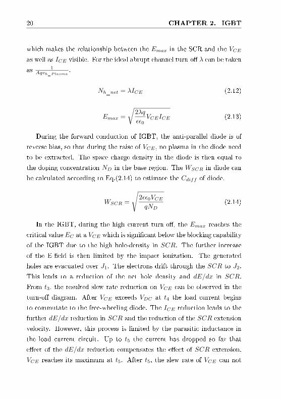
20 CHAPTER 2. IGBT
which makes the relationship between the Emax in the SCR and the VCE
as well as ICE visible. For the ideal abrupt channel turn-o λ can be taken
as 1Aqvh_Plasma
.
Nh_net = λICE (2.12)
Emax =
√2λq
ϵϵ0VCEICE (2.13)
During the forward conduction of IGBT, the anti-parallel diode is of
reverse bias, so that during the raise of VCE , no plasma in the diode need
to be extracted. The space charge density in the diode is then equal to
the doping concentration ND in the base region. The WSCR in diode can
be calculated according to Eq.(2.14) to estimate the Cdiff of diode.
WSCR =
√2ϵϵ0VCE
qND(2.14)
In the IGBT, during the high current turn-o, the Emax reaches the
critical value EC at a VCE which is signicant below the blocking capability
of the IGBT due to the high hole-density in SCR. The further increase
of the E-eld is then limited by the impact ionization. The generated
holes are evacuated over J1. The electrons drift through the SCR to J2.
This leads to a reduction of the net hole density and dE/dx in SCR.
From t3, the resulted slew rate reduction on VCE can be observed in the
turn-o diagram. After VCE exceeds VDC at t4 the load current begins
to commutate to the free-wheeling diode. The ICE reduction leads to the
further dE/dx reduction in SCR and the reduction of the SCR extension
velocity. However, this process is limited by the parasitic inductance in
the load current circuit. Up to t5 the current has dropped so far that
eect of the dE/dx reduction compensates the eect of SCR extension.
VCE reaches its maximum at t5. After t5, the slew rate of VCE can not
2.4. POSSIBLE RF-OSCILLATIONS 21
remain positive. From t5 to t6 VCE decreases rapidly to VDC . Up to t7,
the residual plasma is evacuated by the so-called tail current. Just by t7,
SCR reaches the eld stop layer. The tail current gets rapidly to zero and
causes a second peak on the VCE .
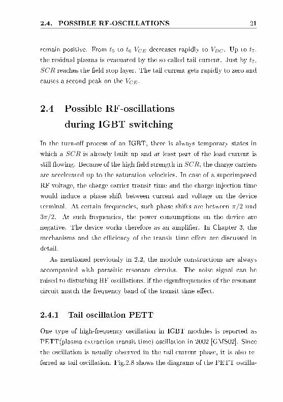
2.4 Possible RF-oscillations
during IGBT switching
In the turn-o process of an IGBT, there is always temporary states in
which a SCR is already built up and at least part of the load current is
still owing. Because of the high eld strength in SCR, the charge carriers
are accelerated up to the saturation velocities. In case of a superimposed
RF-voltage, the charge carrier transit time and the charge injection time
would induce a phase shift between current and voltage on the device
terminal. At certain frequencies, such phase shifts are between π/2 und
3π/2. At such frequencies, the power consumptions on the device are
negative. The device works therefore as an amplier. In Chapter 3, the
mechanisms and the eciency of the transit time eect are discussed in
detail.
As mentioned previously in 2.2, the module constructions are always
accompanied with parasitic resonant circuits. The noise signal can be
raised to disturbing HF-oscillations, if the eigenfrequencies of the resonant
circuit match the frequency band of the transit time eect.
2.4.1 Tail oscillation PETT
One type of high-frequency oscillation in IGBT modules is reported as
PETT(plasma extraction transit time) oscillation in 2002 [GMS02]. Since
the oscillation is usually observed in the tail-current phase, it is also re-
ferred as tail oscillation. Fig.2.8 shows the diagrams of the PETT oscilla-
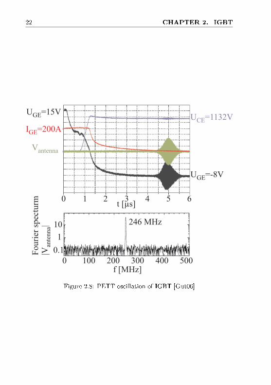
22 CHAPTER 2. IGBT
U =1132VCE
I =200AGE
U =15VGE
Fouri
er s
pec
turm
|V|
ante
nna 10
0.1
1
0 200100 300 500400f [MHz]
0 21 3 54t [µs]
6
U =-8VGE
246 MHz
Vantenna
Figure 2.8: PETT oscillation of IGBT [Gut06]
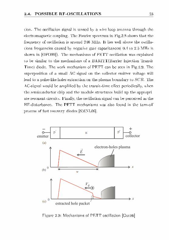
2.4. POSSIBLE RF-OSCILLATIONS 23
tion. The oscillation signal is sensed by a wire loop antenna through the
electromagnetic coupling. The Fourier spectrum in Fig.2.8 shows that the
frequency of oscillation is around 246 MHz. It lies well above the oscilla-
tions frequencies caused by negative gate capacitances( 0.4 to 2.5 MHz is
shown in [OFO99]). The mechanisms of PETT oscillation was explained
to be similar to the mechanisms of a BARITT(Barrier Injection Transit
Time) diode. The work mechanism of PETT can be seen in Fig.2.9. The
superposition of a small AC-signal on the collector-emitter voltage will
lead to a pulse-like holes extraction on the plasma boundary to SCR. The
AC-signal would be amplied by the transit-time eect periodically, when
the semiconductor chip and the module structures build up the appropri-
ate resonant circuits. Finally, the oscillation signal can be perceived as the
HF-disturbance. The PETT mechanisms was also found in the turn-o
process of fast recovery diodes [SMNL06].
electron-holes plasma
estracted hole packet
emitter collector
Vd
E
Figure 2.9: Mechanisms of PETT oscillation [Gut06]
24 CHAPTER 2. IGBT
There are generally two methods to suppress oscillations. The rst one
is to integrate power consumers into the resonant circuit. The power con-
sumer may be resistance in the line, which aects all frequencies. It may
also be the resistive coating on the conductor-line and is especially eec-
tive for high-frequency signals. Energy of the HF-signal can be extracted
also by a resistive conductor adjacent to the resonant circuit. The HF-
power is converted to heat by eddy current in such conductor [SGMM03]
[SGMM02]. The second method of the oscillation suppression is to mis-
match the eigenfrequencies between the amplier and the resonant circuits.
The emitter cross wire-bonding between parallel IGBTs has already
been patented in 1995 as a countermeasure to HF-oscillations during IGBT
turn-o as shown here in Fig.2.10. During switching o of modules with
paralleled IGBT chips (3,4), high frequency oscillation can cause the elec-
tromagnetic interference and the destruction of the chips can still not be
excluded. These oscillations can be prevented by the direct emitter wire-
bonding (14) between the adjacent chips. The cross wire-bondings reduce
the inductance between the adjacent IGBTs and thus the resonant circuits
are out of tune. There are also proposed solutions by increasing the in-
ductance of the resonant circuit to suppress PETT-oscillation [TKY+98].
This usually means the increasing of inductance in the commutation path
of the load current. Such inductance is generally unfavourable for high-
performance power modules. Additional parasitic capacitances and induc-
tance can also be integrated on the DCB-layout to mismatch the eigenfre-
quencies [Mou01a]. Countermeasures to PETT-oscillation are summarized
in chapter 5 of [Gut06].
Although the PETT-oscillation in the tail current phase is a dynamic
process, it shows certain quasi-stationary characteristics. The IGBT has
taken over the entire DC-link voltage before PETT-oscillation appears.
The collector-emitter voltage remains almost unchanged during PETT-
oscillation. The SCR capacitance of IGBT- and diode-chip as well as the
2.4. POSSIBLE RF-OSCILLATIONS 25
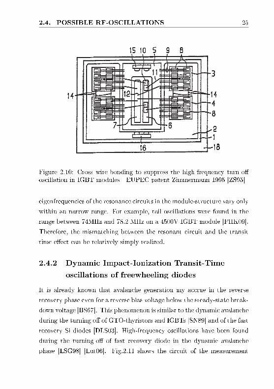
Figure 2.10: Cross wire-bonding to suppress the high-frequency turn-ooscillation in IGBT modules - EUPEC patent Zimmermann 1995 [ZS95]
eigenfrequencies of the resonance circuits in the module-structure vary only
within an narrow range. For example, tail oscillations were found in the
range between 74MHz and 78.2 MHz on a 4500V IGBT module [FHK09].
Therefore, the mismatching between the resonant circuit and the transit
time eect can be relatively simply realized.
2.4.2 Dynamic Impact-Ionization Transit-Time
oscillations of freewheeling diodes
It is already known that avalanche generation my accrue in the reverse
recovery phase even for a reverse bias voltage below the steady-state break-
down voltage [BS67]. This phenomenon is similar to the dynamic avalanche
during the turning o of GTO-thyristors and IGBTs [SN89] and of the fast
recovery Si diodes [DLS03]. High-frequency oscillations have been found
during the turning-o of fast recovery diode in the dynamic avalanche
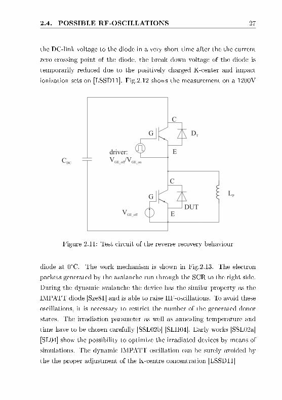
phase [LSG98] [Lut06]. Fig.2.11 shows the circuit of the measurement
26 CHAPTER 2. IGBT
setup to test the reverse recovery behaviour of the freewheeling diode in
the IGBT Module by double pulse mode. The top side IGBT of the half
bridge is actively switched with double pulse during the bottom IGBT is
kept turned-o. The load current in Lp is adjusted by the VDC and the
rst pulse width. After the rst pulse, the top IGBT is in o-state and
the bottom freewheeling diode (DUT) is loaded with the current in LP .
As the top IGBT is turned-on again, the reverse recovery characteristic of
the freewheeling diode occurs. The dynamic oscillation is observed after
the recovery current peak and during the tail current phase of the diode.
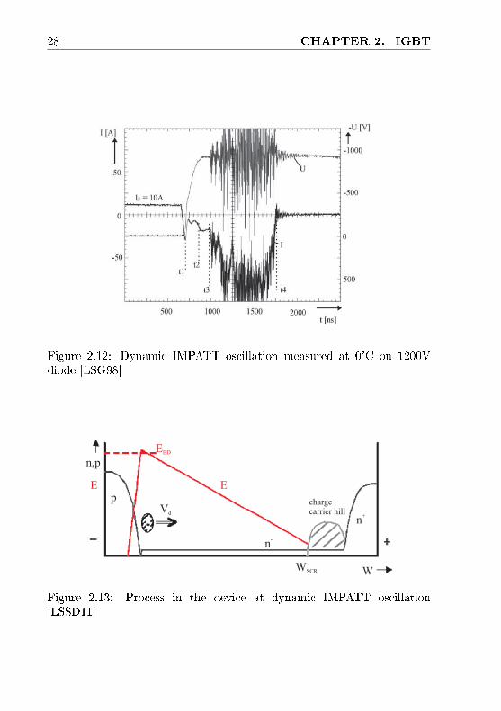
Fig.2.12 shows the measurement on the 1200V diode at 0°C [LSG98].
After the Reverse recovery current peak (time point t1) the reverse current
decreases. Between t1 and t2, the voltage climbs up close to the value of
the DC-link voltage , while the tail current ows in the diode. After t2 a
current hump grows from the tail current. This hump occurs only if the
DC-link voltage is above 910V. The further increase in the DC-link voltage
to 930V eects that a high reverse current suddenly shoots up from the
current hump whose amplitude is a multiple of the reverse recovery current
peak. A high frequency oscillation in the range >500 MHz is superimposed.
After some 100ns(t4), the oscillation is nished. A reduction of the voltage
by only 1 or 2 V, or an increase of the temperature by 1 or 2°C, removes
the eect [LSG98].
The dynamic IMPATT oscillation is caused by the K-centre, which
is created at irradiation of the semiconductor with high-energy particles
[LSG98] for example in the Controlled Axial Liefetime (CAL) technology
[LS94] [SL04]. The K-center has the characteristic of a temporary donor
and is positively charged during the forward conduction. After the voltage
has changed its polarity the K-centre need to be discharged. The time
constant of the discharge process is temperature dependent. It is ca. 100ns
at 400K and is in the order of some microseconds at temperatures below
300K [LSSD11]. Especially for low temperature, when the IGBT applies
2.4. POSSIBLE RF-OSCILLATIONS 27
the DC-link voltage to the diode in a very short time after the the current
zero-crossing point of the diode, the break down voltage of the diode is
temporarily reduced due to the positively charged K-center and impact
ionization sets on [LSSD11]. Fig.2.12 shows the measurement on a 1200V
CDC
G
C
E
DUT
driver:V /VGE_off GE_on
VGE_off
LP
DT
G
C
E
Figure 2.11: Test circuit of the reverse recovery behaviour
diode at 0°C. The work mechanism is shown in Fig.2.13. The electron
packets generated by the avalanche run through the SCR to the right side.
During the dynamic avalanche the device has the similar property as the
IMPATT diode [Sze81] and is able to raise HF-oscillations. To avoid these
oscillations, it is necessary to restrict the number of the generated donor
states. The irradiation parameter as well as annealing temperature and
time have to be chosen carefully [SSL02b] [SLH04]. Early works [SSL02a]
[SL04] show the possibility to optimize the irradiated devices by means of
simulations. The dynamic IMPATT oscillation can be surely avoided by
the the proper adjustment of the K-centre concentration [LSSD11]
28 CHAPTER 2. IGBT
Figure 2.12: Dynamic IMPATT oscillation measured at 0°C on 1200Vdiode [LSG98]
EBD
E
WSCR W
Vd
pE
n,p
n+
n-
chargecarrier hill
Figure 2.13: Process in the device at dynamic IMPATT oscillation[LSSD11]
2.4. POSSIBLE RF-OSCILLATIONS 29
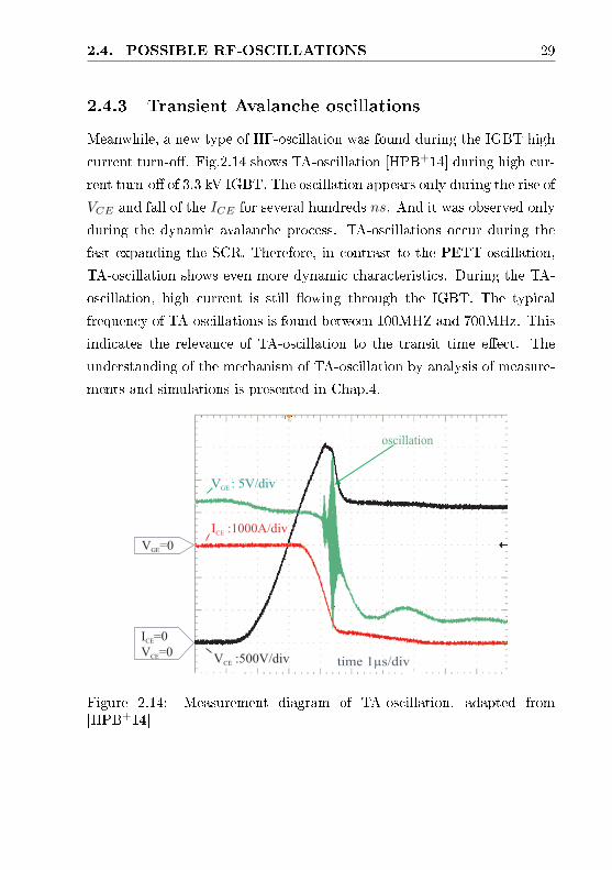
2.4.3 Transient Avalanche oscillations
Meanwhile, a new type of HF-oscillation was found during the IGBT high
current turn-o. Fig.2.14 shows TA-oscillation [HPB+14] during high cur-
rent turn-o of 3.3 kV IGBT. The oscillation appears only during the rise of
VCE and fall of the ICE for several hundreds ns. And it was observed only
during the dynamic avalanche process. TA-oscillations occur during the
fast expanding the SCR. Therefore, in contrast to the PETT-oscillation,
TA-oscillation shows even more dynamic characteristics. During the TA-
oscillation, high current is still owing through the IGBT. The typical
frequency of TA-oscillations is found between 100MHZ and 700MHz. This
indicates the relevance of TA-oscillation to the transit time eect. The
understanding of the mechanism of TA-oscillation by analysis of measure-
ments and simulations is presented in Chap.4.
I :1000A/divCE
V : 5V/divGE
V :500V/divCE time 1µs/div
oscillation
ICE=0
V =0CE
V =0GE
Figure 2.14: Measurement diagram of TA-oscillation, adapted from[HPB+14]

30 CHAPTER 2. IGBT
Chapter 3
Mechanisms of Transit time
eect and RF-oscillations in
IGBT Modules
When a point charge is moving in a conductor system, the terminal current
of the conductor system is determined by the movement of the point charge
but not the charge carriers arriving to the electrodes [Sho38]. This is
known as Ramo-Shockley theorem. Using this theorem the transit time
eect of charge carriers through the space charge region can be explained.
IMPATT diodes and BARITT diodes are the devices based on the similar
principle corresponding to the transit time eect. In the diodes, a space
charge region (SCR) is formed at a reverse biased pn-junction by a DC-
voltage. The charge injection into the SCR can be induced by a AC voltage
supplied additionally to the DC voltage. In a IMPATT diode, the Emax
is set to just below the EC so that the additional AC-voltage would drive
the Emax to exceed EC . The charge injection is caused by the avalanche
generation. In the BARITT diodes, there is a forward biased pn-junction
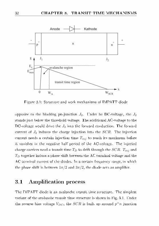
32 CHAPTER 3. TRANSIT TIME MECHANISMS
E
x
-
p+
n+n
+
J1 J2
Ec
0 WAWSCR
avalanche region
transit time region
Emax
Anode Kathode
Figure 3.1: Structure and work mechanisms of IMPATT diode
opposite to the blocking pn-junction J2. Under he DC-voltage, the J2
stands just below the threshold voltage. The additional AC-voltage to the
DC-voltage would drive the J2 into the forward conduction. The forward
current of J2 induces the charge injection into the SCR. The injection
current needs a certain injection time Tinj to reach its maximum before
it vanishes in the negative half period of the AC-voltage. The injected
charge carriers need a transit time TD to drift through the SCR. Tinj and
TD together induce a phase shift between the AC terminal voltage and the
AC terminal current of the diodes. In a certain frequency range, in which
the phase shift is between 1π/2 and 3π/2, the diode acts as amplier.
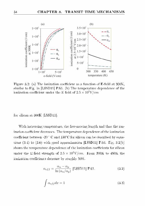
3.1 Amplication process
The IMPATT diode is an avalanche transit time structure. The simplest
variant of the avalanche transit time structure is shown in Fig. 3.1. Under
the reverse bias voltage VDC , the SCR is built up around p+n junction
3.1. AMPLIFICATION PROCESS 33
J1. On the p+ side, the E-eld decreases steeply to zero. Due to the weak
doping level of the n region, the SCR stretches wide into it. At the oper-
ation point, the VDC is adjusted just below the breakdown voltage. The
maximum eld strength Emax directly at the position J1 is just below the
critical eld strength Ec. In operation, an AC voltage VAC is superim-
posed on VDC . In the positive half cycle of VAC , the structure is driven
into avalanche. Electron-hole pairs are generated near J1. The holes are
extracted through p+ to anode during the electrons have to drift through
the transit-time region to the cathode side. The E-eld in the drift region
is adjusted high enough so that the drift velocity of the charge carriers
reach the saturation velocities υs. As already described in Chap.2, a sim-
ilar avalanche transit-time structure is formed from t3 (Abb. 2.6) during
turn-o of the IGBT.
3.1.1 Avalanche breakdown
Under the strong E-eld, electrons / holes can be so strongly accelerated
that they gather sucient energy on their free-moving length to generate
new electron-hole pairs through the collision with the next atomic lattice.
The ionization coecient αn,p indicates the number of electron-hole pairs
generated by an electron / hole on the distance of 1cm. The structure
comes into breakdown, when the charge carrier multiplication in the SCR
leads to a innity current. The avalanche breakdown criterion is given by
equation (3.1) in [Sze81] S.100.
∫ W
0
αn exp
(−∫ W
x
(αn − αp) dx′
)dx = 1 (3.1)
The equation (3.1) can be simplied to (3.3) using the denition of the
eective ionization coecient αeff in equation (3.2) [LSSD11] P.62. For
the E-eld strength over 1 × 10⁵ , the ionization rate increases exponen-
tially. Fig. 3.2(a) shows the eld dependence of the ionization coecient
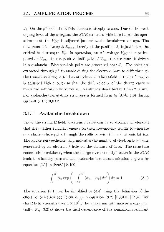
34 CHAPTER 3. TRANSIT TIME MECHANISMS
ion
izat
ion
co
effi
cien
t (1
/cm
)at
30
0K
1×100
1×101
1×10²
1×10³
1×10⁴
1×10⁵
1×10⁵
5×10⁵
0
5×10²
1×10³
1.5×10³
2.0×10³
2.5×10³
3.0×10³
3.5×10³
300 350 400 450
αn
αp
αeff
αn
αp
αeff
e-field (V/cm)
ion
izat
ion
co
effi
cien
t(1
/cm
)
at 2
.5×
10
V/c
m5
temperature (K)
(a) (b)
Figure 3.2: (a) The ionization coecient as a function of E-eld at 300K,similar to Fig. in [LSSD11] P.65. (b) The temperature dependence of theionization coecient under the E-eld of 2.5× 10⁵V/cm
for silicon at 300K [LSSD11].
With increasing temperature, the free-moving length and thus the ion-
ization coecient decreases. The temperature dependence of the ionization
coecient between -20 ° C and 150°C for silicon can be described by equa-
tions (3.4) to (3.6) with good approximation [LSSD11] P.64. Fig. 3.2(b)
shows the temperature dependence of the ionization coecients for silicon
under the E-eld strength of 2.5 × 10⁵V/cm. From 300K to 450K the
ionization coecients decrease by roughly 50%.
αeff =αn − αp
ln (αn/αp)[LSSD11] P.61. (3.2)
∫αeffdx = 1 (3.3)
3.1. AMPLIFICATION PROCESS 35
αn = 1.1× 10⁶ · exp(−1.46× 10⁶ + 1100 (T − 300K)
E
)cm−1 (3.4)
αp = 2.1× 10⁶ · exp(−2.2× 10⁶ + 1100 (T − 300K)
E
)cm−1 (3.5)
αeff∼= 1.06× 10⁶ · exp
(−1.68× 10⁶ + 1100 (T − 300K)
E
)cm−1 (3.6)
The avalanche region is generally dened as eq. (3.7), where the integral
of the ionisation coecient along the avalanche region reach 0.95 [Sze81]
P.573. ∫ WA
0
αeffdx = 0.95 (3.7)
3.1.2 Amplication eciency
Fig. 3.3 shows the diagram of terminal voltage, charge injection and the
induced current of the transit time structure. The terminal voltage is a
result of the AC-voltage override VRF sin(ωt) to the VDC .
VT = VDC + VRF sinωt (3.8)
According to the "`Ramo-Shockley theorem"', the diode current is equal
to the average convection current through out the drift region ([Pau81]
P.315). When a charge packet of Q is injected into the SCR at the position
of WA and drifts with the velocity of vQ, as shown in Fig.3.1, the inducing
current Jind on the terminal can be described by Eq.3.9 [EH98] P.354.
Jind =Q
WSCR
(υQ − WA
WSCR
dWSCR
dt
)(3.9)
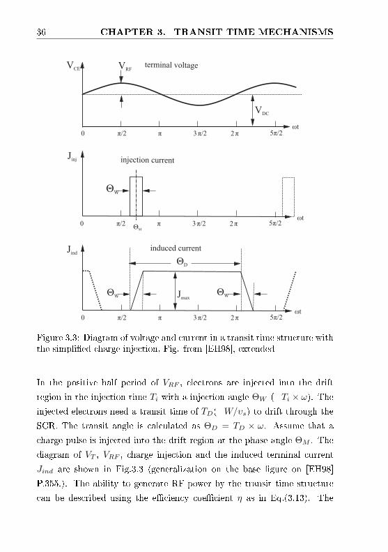
36 CHAPTER 3. TRANSIT TIME MECHANISMS
induced current
0 π 3π/2 2 ππ/2
VRFVCE
VDC
injection current
ΘW
ΘM
ΘW
ΘD
ωt
ΘW
5π/2
Jinj
Jind
Jmax
ωt
ωt
0 π 3π/2 2 ππ/2 5π/2
0 π 3π/2 2 ππ/2 5π/2
terminal voltage
Figure 3.3: Diagram of voltage and current in a transit time structure withthe simplied charge injection, Fig. from [EH98], extended
In the positive half period of VRF , electrons are injected into the drift
region in the injection time Ti with a injection angle ΘW (=Ti × ω). The
injected electrons need a transit time of TD(=W/υs) to drift through the
SCR. The transit angle is calculated as ΘD = TD × ω. Assume that a
charge pulse is injected into the drift region at the phase angle ΘM . The
diagram of VT , VRF , charge injection and the induced terminal current
Jind are shown in Fig.3.3 (generalization on the base gure on [EH98]
P.355.). The ability to generate RF-power by the transit time structure
can be described using the eciency coecient η as in Eq.(3.13). The
3.1. AMPLIFICATION PROCESS 37
eciency coecient is the ratio of the RF-power generation to the total
power consumption which is drawed from the DC-voltage source VDC . The
introduction steps are involved in Appendix A
JDC =1
2π
∫ ΘD+ΘM+ΘW /2
ΘM−ΘW /2
Jind (ωt) d(ωt) (3.10)
PDC = JDCVDC (3.11)
PRF = − A
2π
∫ ΘD+ΘM+ΘW /2
ΘM−ΘW /2
Jind (ωt)VRF sin(ωt)d(ωt) (3.12)
η =PRF
PDC=
VRF
VDC
sin(ΘW
2)
ΘW
2
cos (ΘM +ΘD)− cosΘM
ΘD(3.13)
The injection dependent eciency coecient η1 (3.14) and the transit time
dependent eciency coecient η2 (3.15) can be eliminated out of η. η1 gets
its maximum as the ΘW goes to Zero. The ecient coecient favoured
from the short injection pulse. In an IMPATT diode, the charge injection
reach its maximum roughly at ΘM = π. For the BARITT diode, the max-
imal charge injection happens at ΘM = π/2. The optimal width of drift
region and the corresponding transit angle can therefore be estimated for
the most eective Rf-power conversion. For IMPATT diode, the optimal
transit angle ΘD ≈ 3π/4. And for BARITT diode the optimal transit
38 CHAPTER 3. TRANSIT TIME MECHANISMS
angle ist found to be ΘD ≈ 3π/2 [EH98] P.355.
η1(ΘW ) =sin(
ΘW
2)
ΘW
2
(3.14)
η2(ΘD) =cos (ΘM +ΘD)− cosΘM
ΘD(3.15)
As Eq.(3.13) is derived without the interval limitation of 2π, it can be
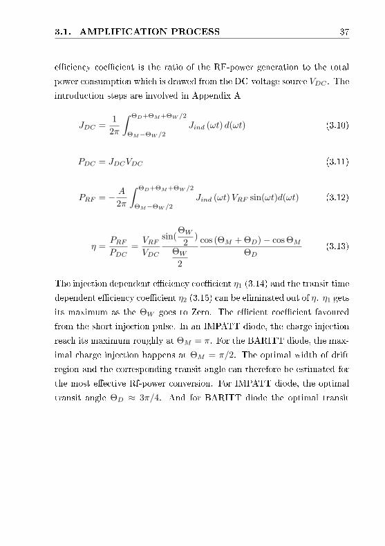
applied to the case of wide drift regions as in IGBT (ΘM +ΘD ≥ 2π). In
the frequency range that the transit angle lies in (2n−1)π < ΘD(2n−1)π,
the BARITT and the corresponding PETT mechanisms have the ability to
generate RF-power. The IMPATT mechanism can theoretically generate
Rf-power in the whole frequency range. As can be seen in Fig.3.4, η2 has
at least a second and a third peak value in addition to its maximum. The
peak value of η2 reduces with the increase of the transit angle, but the
second peak value of IMPATT mechanism is still as high as the maximum
of BARITT structure. The PETT and BARITT mechanism shows the
damping eect as long as the the frequencies are low [Sil14]. The drift
velocity of electrons and holes (υdn, υdp) can be derived on the basis of
the measurement of electron and hole drift velocity in Silicon [CMMO75].
The equations Eq.(3.16)and Eq.(3.17) describe the dependencies on tem-
perature and E-eld [Bal79] P.10.
υdn =1.42× 10⁹T−2.42E
[1 + (E/1.01T 1.55)2.57×10⁻²T 0.66 ](2.57×10−2T 0.66)−1 (3.16)
υdp =1.31× 10⁹T−2.2E
[1 + (E/1.24T 1.68)0.46×10⁻²T 0.17 ](0.46×10−2T 0.17)−1 (3.17)
Under the assumption of a triangle E-eld distribution and the maximal
E-eld of 2× 10⁵V/cm, the eective velocities of electrons and holes (υdn,
3.1. AMPLIFICATION PROCESS 39
-1.2
-1
-0.8
-0.6
-0.4
-0.2
0
0.2
0.4
0.6
0.8
1
0π 1π 2π 3π 4π 5π 6π 7π
η2 IMPATT
η2 BARITT/ PETT
drift angle ΘD
effi
cien
cyη
2F1IM ,F2IM
F1BA
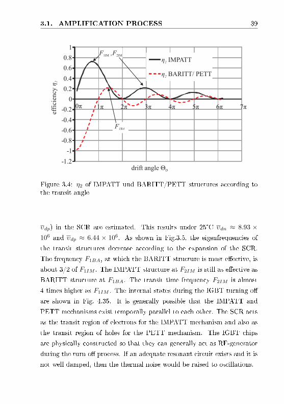
Figure 3.4: η2 of IMPATT und BARITT/PETT structures according tothe transit angle
υdp) in the SCR are estimated. This results under 25°C υdn ≈ 8.93 ×10⁶ and υdp ≈ 6.44 × 10⁶. As shown in Fig.3.5, the eigenfrequencies of
the transit structures decrease according to the expansion of the SCR.
The frequency F1BA, at which the BARITT structure is most eective, is
about 3/2 of F1IM . The IMPATT structure at F2IM is still as eective as
BARITT structure at F1BA. The transit time frequency F2IM is almost
4 times higher as F1IM . The internal states during the IGBT turning-o
are shown in Fig. 4.35. It is generally possible that the IMPATT and
PETT mechanisms exist temporally parallel to each other. The SCR acts
as the transit region of electrons for the IMPATT mechanism and also as
the transit region of holes for the PETT mechanism. The IGBT chips
are physically constructed so that they can generally act as RF-generator
during the turn-o process. If an adequate resonant circuit exists and it is
not well damped, then the thermal noise would be raised to oscillations.
40 CHAPTER 3. TRANSIT TIME MECHANISMS
W (µm)SCR
eigen
fre
quen
cy (
Hz)
0
5.0×10⁹
1.0×10⁹
1.5×10⁹
2.0×10⁹
2.5×10⁹
3.0×10⁹
0 100 200 300 400 500
F1IM
F2IM
F1BA
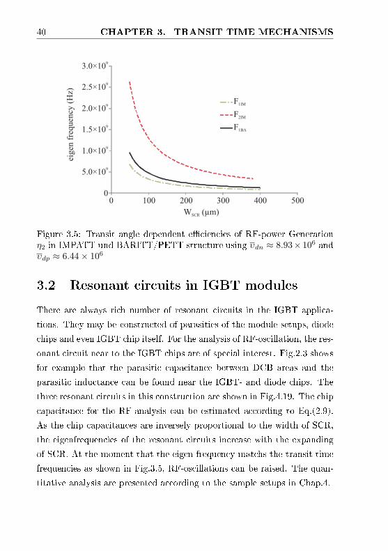
Figure 3.5: Transit angle dependent eciencies of RF-power Generationη2 in IMPATT und BARITT/PETT structure using υdn ≈ 8.93× 10⁶ andυdp ≈ 6.44× 10⁶
3.2 Resonant circuits in IGBT modules
There are always rich number of resonant circuits in the IGBT applica-
tions. They may be constructed of parasitics of the module setups, diode
chips and even IGBT chip itself. For the analysis of RF-oscillation, the res-
onant circuit near to the IGBT chips are of special interest. Fig.2.3 shows
for example that the parasitic capacitance between DCB areas and the
parasitic inductance can be found near the IGBT- and diode chips. The
three resonant circuits in this construction are shown in Fig.4.19. The chip
capacitance for the RF-analysis can be estimated according to Eq.(2.9).
As the chip capacitances are inversely proportional to the width of SCR,
the eigenfrequencies of the resonant circuits increase with the expanding
of SCR. At the moment that the eigen frequency matchs the transit time
frequencies as shown in Fig.3.5, RF-oscillations can be raised. The quan-
titative analysis are presented according to the sample setups in Chap.4.
Chapter 4
Analysis of Transient
Avalanche oscillation
Under high current density, high frequency oscillation signals are found on
the trace of gate-emitter voltage during the turning o of 3.3 kV IGBTs
as shown in Fig. 2.14. This leads to the presumption that gate capaci-
tance and the Miller-feedback could be responsible for the this oscillation.
However this presumption is disproved by the measurements and simula-
tions introduced in this chapter. Moreover the RF-signals are found to
be emitted by the emitter wire bonds. As this oscillation occurs only
transiently during the dynamic avalanche of the IGBT, it is called TA-
oscillation in this work. The resonant circuits of TA-oscillations can be
localized nearby the IGBT chips. The parasitics extraction of setups on
DCB and the analytical estimations of IGBT and diode chip-capacitance
allow the quantitative analysis of the resonant circuits according to the
eigenfrequencies. The mechanisms of TA-oscillation are illustrated corre-
sponding to the transit time eect and are veried by device simulations.
42 CHAPTER 4. ANALYSIS OF TA-OSCILLATION
4.1 Measurement of TA-oscillations
Systematic measurements are accomplished on 3.3kV IGBT modules and
substrates setups to nd out the source and the relevant parameters of
TA-oscillations.
4.1.1 Measurement of TA-oscillation on IGBT mod-
ules
TA-oscillations are rst observed on an 3.3kV IGBT module under de-
velopment, in which 24×IGBT chips are parallel arranged and act as a
single switch. Two modules are series connected to a half-bridge for the
dynamic characterization as shown in Fig.2.4. The hardware conguration
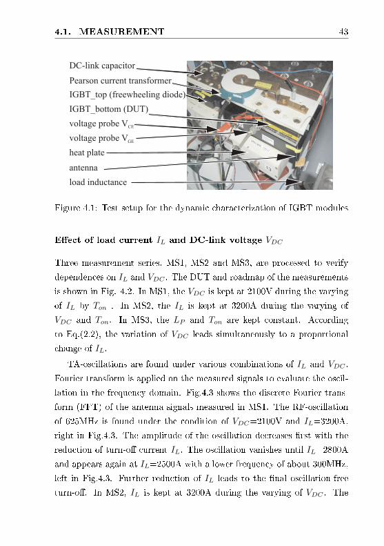
of the dynamic characterization is represented in Fig.4.1. Because of the
high voltage, the dynamic characterizations are generally carried out in a
grounded security box. For the conventional measurements three channels
of oscilloscope are necessary to record VCE , VGE and ICE . A 1000× volt-
age probe is applied for VCE . A 10× voltage probe is applied for VGE .
ICE is converted to voltage signal using a Pearson current transformer.
Additionally to the conventional dynamic module characterization, for the
oscillation analysis, a wire loop is placed near the DUT to capture the RF-
disturbance. Care must be taken for the parasitics in the ground loop in
order to distinguish the real RF-signal and the interferences, see appendix
B.
Similarly to the PETT oscillation, the oscillation frequencies of TA-
oscillation are in the range of several hundreds of MHz. But unlike the
PETT oscillation, TA-oscillation does not appear in the phase of the tail
current. TA-oscillations are found during the dynamic avalanche of the
high current turn-o of the IGBT. As TA-oscillation happens, the DUT is
under high voltage and high current density.
4.1. MEASUREMENT 43
DC-link capacitor
Pearson current transformer
IGBT_top (freewheeling diode)
IGBT_bottom (DUT)
voltage probe VCE
voltage probe V
heat plate
antenna
load inductance
GE
Figure 4.1: Test setup for the dynamic characterization of IGBT modules
Eect of load current IL and DC-link voltage VDC
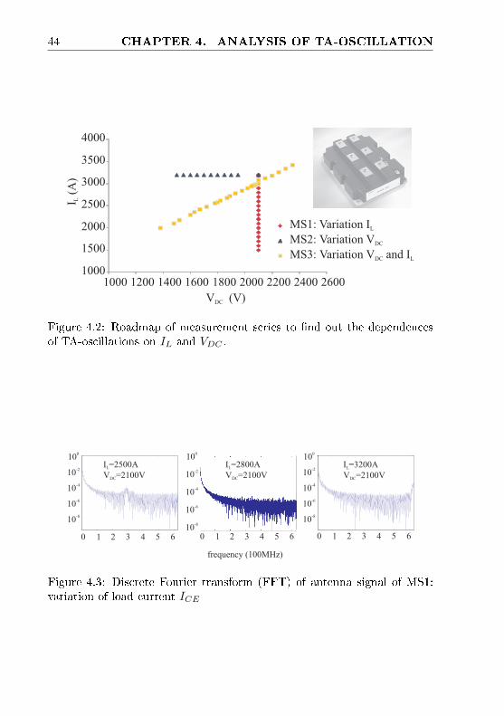
Three measurement series, MS1, MS2 and MS3, are processed to verify
dependences on IL and VDC . The DUT and roadmap of the measurements
is shown in Fig. 4.2. In MS1, the VDC is kept at 2100V during the varying
of IL by Ton . In MS2, the IL is kept at 3200A during the varying of
VDC and Ton. In MS3, the LP and Ton are kept constant. According
to Eq.(2.2), the variation of VDC leads simultaneously to a proportional
change of IL.
TA-oscillations are found under various combinations of IL and VDC .
Fourier transform is applied on the measured signals to evaluate the oscil-
lation in the frequency domain. Fig.4.3 shows the discrete Fourier trans-
form (FFT) of the antenna signals measured in MS1. The RF-oscillation
of 625MHz is found under the condition of VDC=2100V and IL=3200A,
right in Fig.4.3. The amplitude of the oscillation decreases rst with the
reduction of turn-o current IL. The oscillation vanishes until IL=2800A
and appears again at IL=2500A with a lower frequency of about 300MHz,
left in Fig.4.3. Further reduction of IL leads to the nal oscillation-free
turn-o. In MS2, IL is kept at 3200A during the varying of VDC . The
44 CHAPTER 4. ANALYSIS OF TA-OSCILLATION
1000
1500
2000
2500
3000
3500
4000
1000 1200 1400 1600 1800 2000 2200 2400 2600
V (V)DC
M 1: Variation IS L
MS3: Variation V and IDC L
MS2: Variation VDC
I(A
)L
Figure 4.2: Roadmap of measurement series to nd out the dependencesof TA-oscillations on IL and VDC .
0 1 2 3 4 5 6 0 1 2 3 4 5 6
frequency (100MHz)
10-8
10-6
10-4
10-2
100
10-8
10-6
10-4
10-2
100
I =2800A
VL
DC=2100V
I =2500A
VL
DC=2100V
I =3200A
VL
DC=2100V
0 1 2 3 4 5 6
10-8
10-6
10-4
10-2
100
Figure 4.3: Discrete Fourier transform (FFT) of antenna signal of MS1:variation of load current ICE
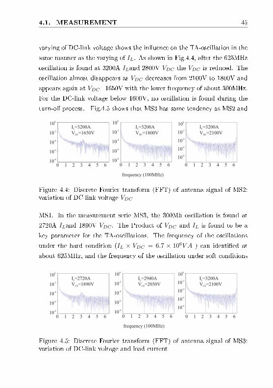
4.1. MEASUREMENT 45
varying of DC-link voltage shows the inuence on the TA-oscillation in the
same manner as the varying of IL. As shown in Fig.4.4, after the 625MHz
oscillation is found at 3200A ILand 2800V VDC the VDC is reduced. The
oscillation almost disappears as VDC decreases from 2100V to 1800V and
appears again at VDC=1650V with the lower frequency of about 300MHz.
For the DC-link voltage below 1600V, no oscillation is found during the
turn-o process. Fig.4.5 shows that MS3 has same tendency as MS2 and
I =3200A
VL
DC=2100V
0 1 2 3 4 5 610
-8
10-6
10-4
10-2
100
I =3200A
VL
DC=1800V
I =3200A
VL
DC=1650V
0 1 2 3 4 5 6 0 1 2 3 4 5 610
-8
10-6
10-4
10-2
100
10-8
10-6
10-4
10-2
100
frequency (100MHz)
Figure 4.4: Discrete Fourier transform (FFT) of antenna signal of MS2:variation of DC-link voltage VDC
MS1. In the measurement serie MS3, the 300Mh oscillation is found at
2720A ILand 1890V VDC . The Product of VDC and IL is found to be a
key parameter for the TA-oscillations. The frequency of the oscillations
under the hard condition (IL × VDC = 6.7 × 10⁶V A ) can identied at
about 625MHz, and the frequency of the oscillation under soft conditions
0 1 2 3 4 5 6
I =3200A
VL
CE=2100V
0 1 2 3 4 5 6
10-8
10-6
10-4
10-2
100
42I =2940A
VL
CE=2050V
0 1 2 3 4 5 610
-8
10-6
10-4
10-2
100
frequency (100MHz)
49
10-8
10-6
10-4
10-2
100
I =2720A
VL
CE=1890V
Figure 4.5: Discrete Fourier transform (FFT) of antenna signal of MS3:variation of DC-link voltage and load current
46 CHAPTER 4. ANALYSIS OF TA-OSCILLATION
0
4×10⁶
8×10⁶
0 Ms1 Ms2 Ms3
hard condition
soft condition
V×
IC
EL
(V×
A)
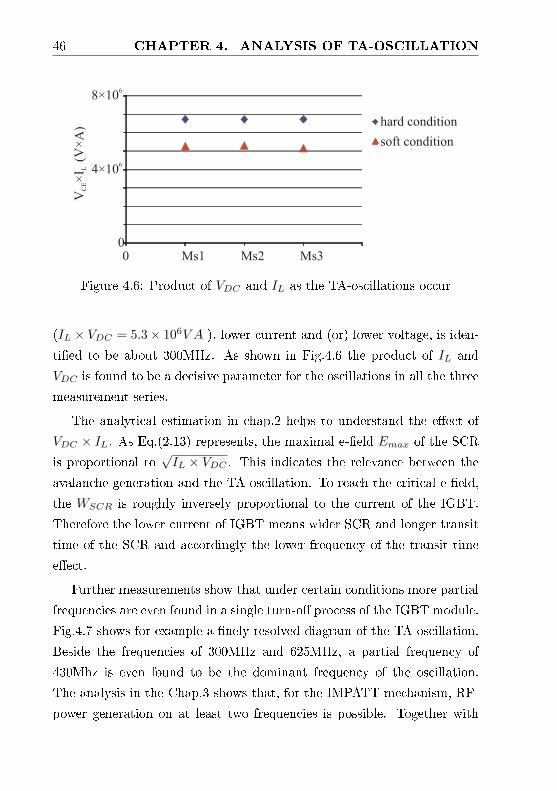
Figure 4.6: Product of VDC and IL as the TA-oscillations occur
(IL × VDC = 5.3× 10⁶V A ), lower current and (or) lower voltage, is iden-
tied to be about 300MHz. As shown in Fig.4.6 the product of IL and
VDC is found to be a decisive parameter for the oscillations in all the three
measurement series.
The analytical estimation in chap.2 helps to understand the eect of
VDC × IL. As Eq.(2.13) represents, the maximal e-eld Emax of the SCR
is proportional to√IL × VDC . This indicates the relevance between the
avalanche generation and the TA-oscillation. To reach the critical e-eld,
the WSCR is roughly inversely proportional to the current of the IGBT.
Therefore the lower current of IGBT means wider SCR and longer transit
time of the SCR and accordingly the lower frequency of the transit time
eect.
Further measurements show that under certain conditions more partial
frequencies are even found in a single turn-o process of the IGBT module.
Fig.4.7 shows for example a nely resolved diagram of the TA-oscillation.
Beside the frequencies of 300MHz and 625MHz, a partial frequency of
430Mhz is even found to be the dominant frequency of the oscillation.
The analysis in the Chap.3 shows that, for the IMPATT mechanism, RF-
power generation on at least two frequencies is possible. Together with
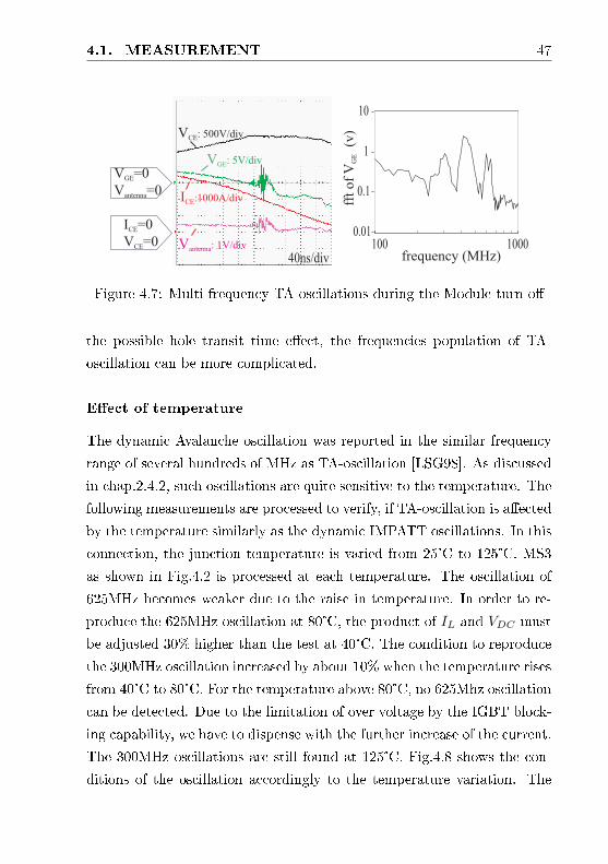
4.1. MEASUREMENT 47
10
0.01
0.1
1
100010040ns/div
fft
of
V(v
)G
E
frequency (MHz)
ICE:1000A/div
VGE: 5V/div
VCE: 500V/div
Vantenna: 1V/div
ICE=0
V =0CE
VGE=0
Vantenna=0
Figure 4.7: Multi frequency TA-oscillations during the Module turn-o
the possible hole transit time eect, the frequencies population of TA-
oscillation can be more complicated.
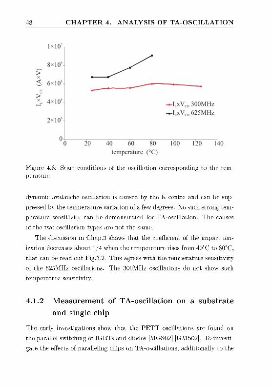
Eect of temperature
The dynamic Avalanche oscillation was reported in the similar frequency
range of several hundreds of MHz as TA-oscillation [LSG98]. As discussed
in chap.2.4.2, such oscillations are quite sensitive to the temperature. The
following measurements are processed to verify, if TA-oscillation is aected
by the temperature similarly as the dynamic IMPATT oscillations. In this
connection, the junction temperature is varied from 25°C to 125°C. MS3
as shown in Fig.4.2 is processed at each temperature. The oscillation of
625MHz becomes weaker due to the raise in temperature. In order to re-
produce the 625MHz oscillation at 80°C, the product of IL and VDC must
be adjusted 30% higher than the test at 40°C. The condition to reproduce
the 300MHz oscillation increased by about 10% when the temperature rises
from 40°C to 80°C. For the temperature above 80°C, no 625Mhz oscillation
can be detected. Due to the limitation of over voltage by the IGBT block-
ing capability, we have to dispense with the further increase of the current.
The 300MHz oscillations are still found at 125°C. Fig.4.8 shows the con-
ditions of the oscillation accordingly to the temperature variation. The
48 CHAPTER 4. ANALYSIS OF TA-OSCILLATION
0
2×10⁶
4×10⁶
6×10⁶
8×10⁶
1×10⁷
0 20 40 60 80 100 120 140
I xV 300MHzL CD
I xV 625MHzL CD
temperature (°C)
I×
V(A
×V
)L
CE
Figure 4.8: Start conditions of the oscillation corresponding to the tem-perature
dynamic avalanche oscillation is caused by the K-centre and can be sup-
pressed by the temperature variation of a few degrees. No such strong tem-
perature sensitivity can be demonstrated for TA-oscillation. The causes
of the two oscillation types are not the same.
The discussion in Chap.3 shows that the coecient of the impact ion-
ization decreases about 1/4 when the temperature rises from 40°C to 80°C,
that can be read out Fig.3.2. This agrees with the temperature sensitivity
of the 625MHz oscillations. The 300MHz oscillations do not show such
temperature sensitivity.
4.1.2 Measurement of TA-oscillation on a substrate
and single chip
The early investigations show that the PETT oscillations are found on
the parallel switching of IGBTs and diodes [MGS02] [GMS02]. To investi-
gate the eects of paralleling chips on TA-oscillations, additionally to the
4.1. MEASUREMENT 49
engineering IGBT module with 24× paralleling IGBTs, measurements on
substrate setups with 4× IGBTs, 2× IGBTs and also on setups with sin-
gle IGBT chip are conducted. The TA-oscillations are even found on the
single IGBT setups. The paralleling of chips is not absolutely necessary
for TA-oscillation.
The following measurements on the substrate setups are carried out
to nd out the critical parameter, the amplier, the resonant circuits of
TA-oscillation.
Eect of RG on substrate
To eliminate the eect of the asymmetry in the gate circuit of the IGBT
Modules, measurements are processed on the substrate setups with much
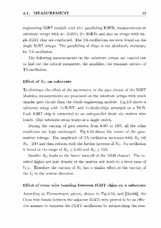
simpler gate circuit than the whole engineering module. Fig.4.9 shows a
substrate setup with 4×IGBT- and 4×diode-chips arranged on a DCB.
Each IGBT chip is connected to an anti-parallel diode via emitter wire
bonds. This substrate setup works as a single switch.
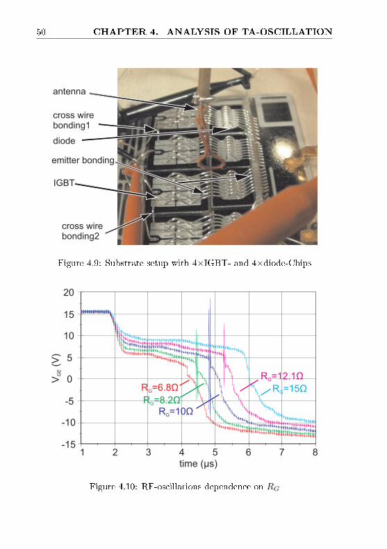
During the varying of gate resistor from 6.8Ω to 15Ω, all the other
conditions are kept unchanged. Fig.4.10 shows the traces of the gate-
emitter voltage. The amplitude of TA-oscillation increases with RG till
RG=10Ω and then reduces with the further increase of RG. No oscillation
is found in the range of RG ≤ 6.8Ω and RG ≥ 15Ω.
Smaller RG leads to the faster turn-o of the MOS channel. The re-
sulted higher net hole density at the emitter side leads to a steep raise of
VCE . Therefore the varying of RG has a similar eect as the varying of
the IL in the reverse direction.
Eect of cross wire bonding between IGBT chips on a substrate
According to Zimmermann patent, shown in Fig.2.10, and [Gut06], the
Cross wire bonds between the adjacent IGBTs were proved to be an eec-
tive manner to suppress the PETT oscillations by mismatching the reso-
50 CHAPTER 4. ANALYSIS OF TA-OSCILLATION
diode
IGBT
antenna
emitter bonding
cross wirebonding1
cross wirebonding2
Figure 4.9: Substrate setup with 4×IGBT- and 4×diode-Chips
1 2 3 4 5 6 7 8time (µs)
-15
-10
-5
0
5
10
15
20
V(V
)G
E
R =6.8G Ω
R =8.2G ΩR =10G Ω
R =12.1G Ω
R =15G Ω
Figure 4.10: RF-oscillations dependence on RG
4.1. MEASUREMENT 51
nant circuit frequency and the PETT frequency. As the TA-oscillations are
found in the similar frequency range as PETT oscillations, the cross wire
bonds were also expected to suppress TA-oscillations. Fig.4.11 shows the
measurements on substrates with dierent cross wire bond congurations.
A 30MHz oscillation is found on the substrate which can be suppressed
by the cross wire bond 1 and 2 between the adjacent IGBTs as shown
in Fig.4.9. The 600MHz oscillation is however not obviously suppressed
by the cross wire bonds. As discussed in Chap.??, during the time the
PETT normally happens, the SCR in IGBT and diode vary only within a
narrow range. The eigenfrequencies of the resonant circuits can be shifted
out of the transit time frequency of PETT mechanism by the cross wire
bond. But the TA-oscillation occurs during the raise of VCE and fall of the
ICE . The SCR is expanding much more dynamically than during PETT
oscillation. During TA-oscillation, because of the expanding of SCR, both
the transit time frequency and the resonant frequencies are changing within
a wide range. This makes it dicult to mismatch the resonant circuit to
the transit time frequency by cross wire bonds.
Eect of chip thickness
In case of the PETT oscillation, the oscillation occurs at the end of the tail
current phase. The SCR has reached almost the eld stop layer on the back
side of the IGBT. Therefore the transit time frequency should be inversely
proportional to the width of the base region of IGBT. To vary the base
region IGBT chip types with identical front side and back side structures
but dierent thickness are processed. Substrates with 4×IGBTs, as shownin Fig.4.9, were setup for each IGBT types. Fig.4.12 shows the discrete
Fourier transform (DFT) of the TA-oscillation signals measured on the
substrate with dierent IGBT chips. Oscillations of 475MHz are found at
all the four chip types. No inuence of the chip thickness can be identied.
This indicates that, as the TA-oscillations occur, the SCRs do not reach
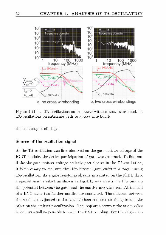
52 CHAPTER 4. ANALYSIS OF TA-OSCILLATION
a. no cross wirebonding b. two cross wirebondings
102
101
100
10-3
10-2
10-1
V in
frequency domainantenne
frequency (MHz)1 10 100 1000
V in
frequency domainantenne
frequency (MHz)1 10 100 1000
10-4
102
101
100
10-3
10-2
10-1
10-4
10-5
V : 500V/divCE
I : 100A/divCE
V : 5V/divGE
V : 1V/divantenna
ICE
=0
V =0CE
V : 500V/divCE
I : 100A/divCE
V : 5V/divGE
V : 1V/divantenna
Vantenna
=0
VGE
=0
Figure 4.11: a. TA-oscillations on substrate without cross wire bond. b.TA-oscillations on substrate with two cross wire bonds
the eld stop of all chips.
Source of the oscillation signal
As the TA-oscillation was rst observed on the gate-emitter voltage of the
IGBT module, the active participation of gate was assumed. To nd out
if the the gate emitter voltage actively participates in the TA-oscillation,
it is necessary to measure the chip internal gate emitter voltage during
TA-oscillation. As a gate resistor is already integrated on the IGBT chip,
a special sense contact as shown in Fig.4.13 was constructed to pick up
the potential between the gate- and the emitter-metallization. At the end
of a BNC cable two feather needles are contacted. The distance between
the needles is adjusted so that one of them contacts on the gate and the
other on the emitter-metallization. The loop area between the two needles
is kept as small as possible to avoid the EMI coupling. For the single chip
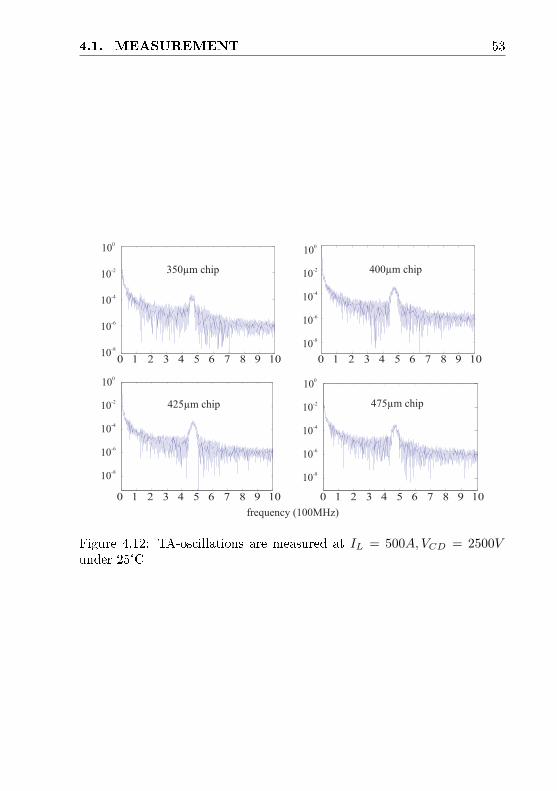
4.1. MEASUREMENT 53
frequency (100MHz)
10-8
10-6
10-4
10-2
100
0 1 2 3 4 5 6 7 8 9 10
10-8
10-6
10-4
10-2
100
0 1 2 3 4 5 6 7 8 9 1010
-8
10-6
10-4
10-2
100
0 1 2 3 4 5 6 7 8 9 10
350µm chip 400µm chip
425µm chip
0 1 2 3 4 5 6 7 8 9 10
10-8
10-6
10-4
10-2
100
475µm chip
Figure 4.12: TA-oscillations are measured at IL = 500A, VCD = 2500Vunder 25°C
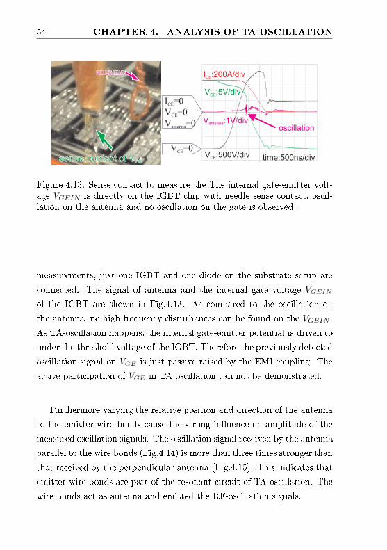
54 CHAPTER 4. ANALYSIS OF TA-OSCILLATION
antenna
Vantenna
:1V/div
V :5V/divGE
sense contact of VGE
V :500V/divCE time:500ns/div
I :200A/divCE
oscillation
V =0CE
I =0CE
VGE
=0
Vantenna
=0
Figure 4.13: Sense contact to measure the The internal gate-emitter volt-age VGEIN is directly on the IGBT chip with needle sense contact, oscil-lation on the antenna and no oscillation on the gate is observed.
measurements, just one IGBT and one diode on the substrate setup are
connected. The signal of antenna and the internal gate voltage VGEIN
of the IGBT are shown in Fig.4.13. As compared to the oscillation on
the antenna, no high frequency disturbances can be found on the VGEIN .
As TA-oscillation happens, the internal gate-emitter potential is driven to
under the threshold voltage of the IGBT. Therefore the previously detected
oscillation signal on VGE is just passive raised by the EMI coupling. The
active participation of VGE in TA-oscillation can not be demonstrated.
Furthermore varying the relative position and direction of the antenna
to the emitter wire bonds cause the strong inuence on amplitude of the
measured oscillation signals. The oscillation signal received by the antenna
parallel to the wire bonds (Fig.4.14) is more than three times stronger than
that received by the perpendicular antenna (Fig.4.15). This indicates that
emitter wire bonds are part of the resonant circuit of TA-oscillation. The
wire bonds act as antenna and emitted the RF-oscillation signals.
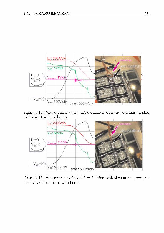
4.1. MEASUREMENT 55
Vantenna: 1V/div
VGE: 5V/div
ICE : 200A/div
VCE: 500V/divtime : 500ns/div
antenna
wire bondings
V =0CE
I =0
=0
CE
antenna
VGE
=0
V
Figure 4.14: Measurement of the TA-oscillation with the antenna parallelto the emitter wire bonds
Vantenna: 1V/div
VGE: 5V/div
ICE : 200A/div
VCE: 500V/divtime : 500ns/div
antenna
wire bondings
V =0CE
I =0
=0
CE
antenna
VGE
=0
V
Figure 4.15: Measurement of the TA-oscillation with the antenna perpen-dicular to the emitter wire bonds
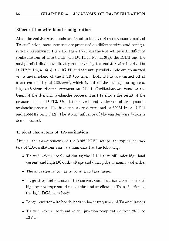
56 CHAPTER 4. ANALYSIS OF TA-OSCILLATION
Eect of the wire bond conguration
After the emitter wire bonds are found to be part of the resonant circuit of
TA-oscillation, measurements are processed on dierent wire bond congu-
rations, as shown in Fig.4.16. Fig.4.16 shows the test setups with dierent
congurations of wire bonds. On DUT1 in Fig.4.16(a), the IGBT and the
anti parallel diode are directly connected by the emitter wire bonds. On
DUT2 in Fig.4.16(b), the IGBT and the anti parallel diode are connected
via a metal island of the DCB top layer. Both DUTs are turned o at
a current density of 130Acm2, which is out of the safe operating area.
Fig. 4.18 shows the measurement on DUT1. Oscillations are found at the
begin of the dynamic avalanche process. Fig.4.17 shows the result of the
measurement on DUT2. Oscillations are found at the end of the dynamic
avalanche process. The frequencies are determined as 600MHz on DUT1
and 155MHz on DUT2. The strong inuence of the emitter wire bonds is
demonstrated.
Typical characters of TA-oscillation
After all the measurements on the 3.3kV IGBT setups, the typical charac-
ters of TA-oscillations can be summarized as the following:
TA-oscillations are found during the IGBT turn-o under high load
current and high DC-link voltage and during the dynamic avalanche.
The gate resistance has to be in a certain range.
Large stray inductance in the current commutation circuit leads to
high over voltage and thus has the similar eect on TA-oscillation as
the high DC-link voltage.
Longer emitter wire bonds leads to lower frequency of TA-oscillations
TA-oscillations are found at the junction temperature from 25°C to
125°C.
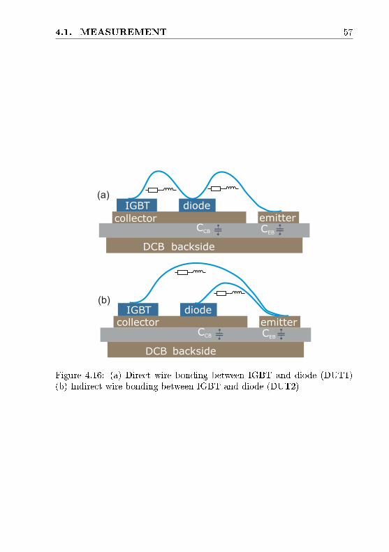
4.1. MEASUREMENT 57
(b)
(a)
IGBT
collector emitter
diode
backsideDCB
CCB C
EB
IGBT
collector emitter
diode
backsideDCB
CCB C
EB
Figure 4.16: (a) Direct wire bonding between IGBT and diode (DUT1)(b) Indirect wire bonding between IGBT and diode (DUT2)
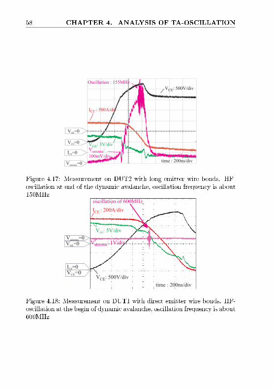
58 CHAPTER 4. ANALYSIS OF TA-OSCILLATION
Oscillation : 155MHz
Vantenna
:
100mV/div
VGE
: 5V/div
ICE
: 500A/div
VCE
: 500V/div
time : 200ns/div
V =0GE
I =0CE
V =0antenna
V =0CE
Figure 4.17: Measurement on DUT2 with long emitter wire bonds. HF-oscillation at end of the dynamic avalanche, oscillation frequency is about150MHz
oscillation of 600MHz
Vantenna
: 1V/div
VGE
: 5V/div
ICE
: 200A/div
VCE
: 500V/div
time : 200ns/div
V =0GE
V =0antenna
I =0CE
VCE
=0
Figure 4.18: Measurement on DUT1 with direct emitter wire bonds. HF-oscillation at the begin of dynamic avalanche, oscillation frequency is about600MHz
4.2. RESONANT CIRCUITS 59
TA-oscillations are found on all chip types with the thickness from
350µm to 475µm, and the frequencies of TA-oscillations are found
to be the same.
Paralleling of IGBTs is not necessary for the TA-oscillations. TA-
oscillations are found also on setups with a single IGBT and a single
diode.
The frequencies of TA-oscillations are found in a frequency band
form 100 to 800MHz for 3.3kv IGBTs. Multi frequencies are found
in a single turn-o process.
The cross wire bond between the adjacent IGBTs is eective for the
suppression of the low frequency oscillation but not eective for the
high frequency oscillation.
The oscillation signals on VGE are proved to be EMI coupling. As
TA-oscillation happens, the internal gate emitter voltage has already
dropped to below the threshold voltage. The gate did not participate
actively in TA-oscillation.
The emission source of the oscillation signals are proven to be the
emitter wire bonds.
4.2 Analysis of the resonant circuits
Resonant circuit is necessary to raise the TA-oscillation. Due to the high
frequency of the oscillation, the resonant circuit must consist of small in-
ductors and capacitors. And they must be located close to the chips, and
the capacitance of the chip itself is expected to participate in the oscilla-
tion. Fig.4.19 shows a schematic illustration of the resonance circuits near
to the IGBT chip with the participation of emitter wire bondings. Three
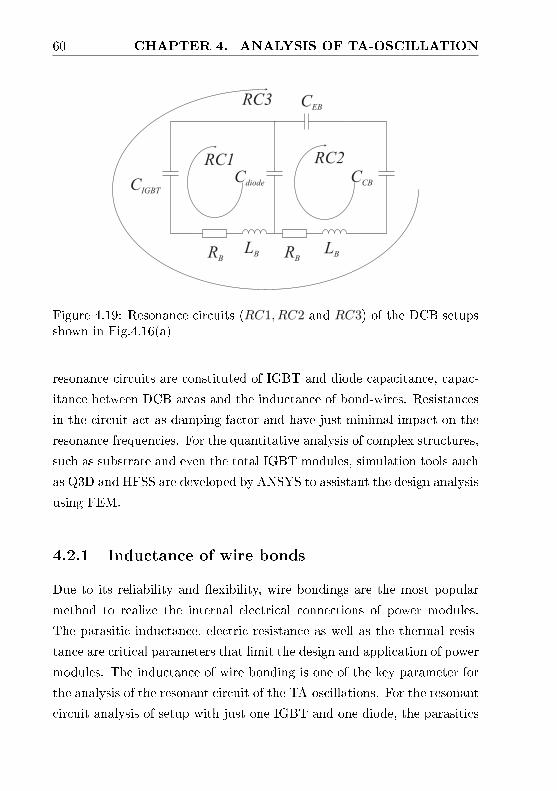
60 CHAPTER 4. ANALYSIS OF TA-OSCILLATION
CIGBT
CCB
Cdiode
CEB
RB
LB
LB R
B
RC3
RC1 RC2
Figure 4.19: Resonance circuits (RC1, RC2 and RC3) of the DCB setupsshown in Fig.4.16(a)
resonance circuits are constituted of IGBT and diode capacitance, capac-
itance between DCB areas and the inductance of bond-wires. Resistances
in the circuit act as damping factor and have just minimal impact on the
resonance frequencies. For the quantitative analysis of complex structures,
such as substrate and even the total IGBT modules, simulation tools auch
as Q3D and HFSS are developed by ANSYS to assistant the design analysis
using FEM.
4.2.1 Inductance of wire bonds
Due to its reliability and exibility, wire bondings are the most popular
method to realize the internal electrical connections of power modules.
The parasitic inductance, electric resistance as well as the thermal resis-
tance are critical parameters that limit the design and application of power
modules. The inductance of wire bonding is one of the key parameter for
the analysis of the resonant circuit of the TA-oscillations. For the resonant
circuit analysis of setup with just one IGBT and one diode, the parasitics
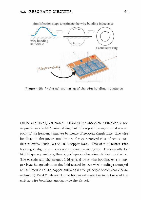
4.2. RESONANT CIRCUITS 61
wire bondinghalf circle
a conductor ring
simplification steps to estimate the wire bonding inductance
Figure 4.20: Analytical estimating of the wire bonding inductance
can be analytically estimated. Although the analytical estimation is not
so precise as the FEM simulations, but it is a practice way to nd a start
point of the frequency analyse by means of network simulations. The wire
bondings in the power modules are always arranged close above a con-
ductor surface such as the DCB-copper layer. One of the emitter wire
bonding conguration is shown for example in Fig.4.9. Theoretically for
high frequency analysis, the copper layer can be taken als ideal conductor.
The electric and the magnet-eld caused by a wire bonding over a cop-
per layer is equivalent to the eld caused by two wire bondings arranged
antisymmetric to the copper surface.(Mirror principle theoretical electro
technique) Fig.4.20 shows the method to estimate the inductance of the
emitter wire bondings analogous to the air coil.
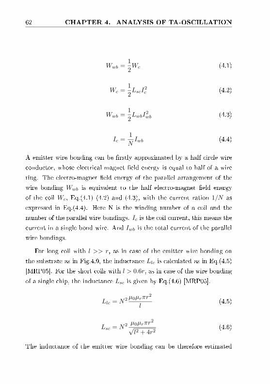
62 CHAPTER 4. ANALYSIS OF TA-OSCILLATION
Wwb =1
2Wc (4.1)
Wc =1
2LscI
2c (4.2)
Wwb =1
2LwbI
2wb (4.3)
Ic =1
NIwb (4.4)
A emitter wire bonding can be rstly approximated by a half circle wire
conductor, whose electrical magnet eld energy is equal to half of a wire
ring. The electro-magnet eld energy of the parallel arrangement of the
wire bonding Wwb is equivalent to the half electro-magnet eld energy
of the coil Wc, Eq.(4.1) (4.2) and (4.3), with the current ration 1/N as
expressed in Eq.(4.4). Here N is the winding number of a coil and the
number of the parallel wire bondings. Ic is the coil current, this means the
current in a single bond wire. And Iwb is the total current of the parallel
wire bondings.
For long coil with l >> r, as in case of the emitter wire bonding on
the substrate as in Fig.4.9, the inductance Llc is calculated as in Eq.(4.5)
[MRP05]. For the short coils with l > 0.6r, as in case of the wire bonding
of a single chip, the inductance Lsc is given by Eq.(4.6) [MRP05].
Llc = N2µ0µrπr2
l(4.5)
Lsc = N2 µ0µrπr2
√l2 + 4r2
(4.6)
The inductance of the emitter wire bonding can be therefore estimated
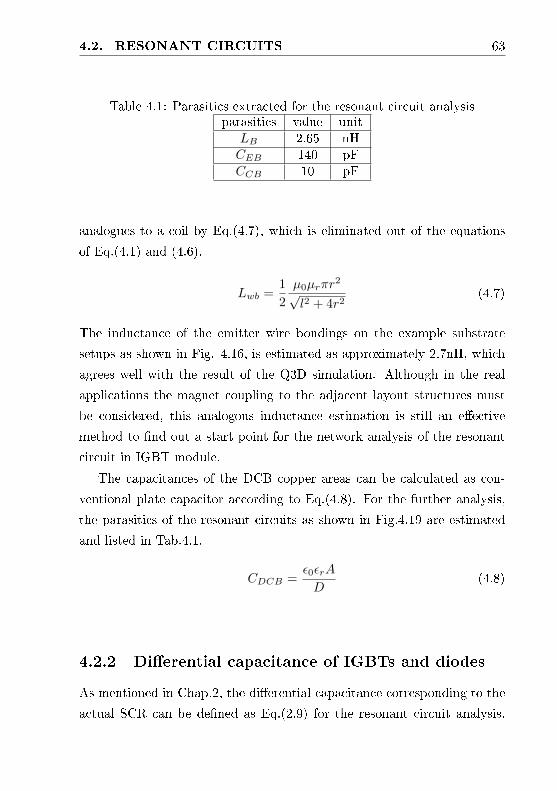
4.2. RESONANT CIRCUITS 63
Table 4.1: Parasitics extracted for the resonant circuit analysisparasitics value unit
LB 2.65 nHCEB 140 pFCCB 10 pF
analogues to a coil by Eq.(4.7), which is eliminated out of the equations
of Eq.(4.1) and (4.6).
Lwb =1
2
µ0µrπr2
√l2 + 4r2
(4.7)
The inductance of the emitter wire bondings on the example substrate
setups as shown in Fig. 4.16, is estimated as approximately 2.7nH, which
agrees well with the result of the Q3D simulation. Although in the real
applications the magnet coupling to the adjacent layout structures must
be considered, this analogous inductance estimation is still an eective
method to nd out a start point for the network analysis of the resonant
circuit in IGBT module.
The capacitances of the DCB copper areas can be calculated as con-
ventional plate capacitor according to Eq.(4.8). For the further analysis,
the parasitics of the resonant circuits as shown in Fig.4.19 are estimated
and listed in Tab.4.1.
CDCB =ϵ0ϵrA
D(4.8)
4.2.2 Dierential capacitance of IGBTs and diodes
As mentioned in Chap.2, the dierential capacitance corresponding to the
actual SCR can be dened as Eq.(2.9) for the resonant circuit analysis.
64 CHAPTER 4. ANALYSIS OF TA-OSCILLATION
The chip capacitances in the resonant circuits as shown in Fig.4.19 are
estimated according to the actual width WSCR of the space charge regions
in the respective chips.
Although IGBTs are so called voltage controlled semiconductor switches,
But their switching processes are indeed current controlled. For the IGBT,
the expanding of the SCR and the ramp up of VCE is mainly limited by
the net hole density, which is determined by the load current and the ratio
between the electron current and hole current in SCR. For the dierent
turn-o conditions, such as dierent RG and dierent IL the expansion
of SCR in the IGBT and the diode can totally dier from each other.
By the assumption that the WSCR in the diode is γ times of the WSCR
in the IGBT, the chip capacitances an the the corresponding resonance
frequencies can be calculated as shown in Fig.4.21 for the analytical un-
derstanding. Due to the absence of plasma in the diode, γ is generally
larger than one. Thereby it is taken into account that chip capacitance
reaches its minimum after the SCR reaches the eld stop layer, and the
active area of the diode is roughly 50% of the IGBT. Higher IL and smaller
RG lead to faster switching process. The faster is the switching process of
the IGBT the larger is γ.
Fig.4.22 shows the diagram of the eigen frequencies of the three res-
onant circuits, estimated according to the WSCRs in IGBT at γ = 2,
together with the transit time frequencies of the corresponding SCR. The
transit time frequencies decrease with the expanding of SCR. The reso-
nance frequencies increase due to the decrease of the chip capacitances
given by (2.9). The intersections of group A and group B in the gure rep-
resent the frequencies, at which the oscillations can be eectively amplied
by the transit time mechanisms. In the frequency range above 1GHz oscil-
lations is theoretically possible, but such oscillations are not jet observed
the real measurements. During the switching o of the channel current,
the ration between the eletron current and hole current in the IGBT and
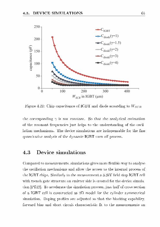
4.3. DEVICE SIMULATIONS 65
capac
itan
ce (
pF
)
0
50
100
150
200
250
0 100 200 300 400
CIGBT
C ( =1)diode γ
C ( =1.5)diode γ
C ( =2)diode γ
C ( =3)diode γ
C ( =4)diode γ
WSCR
in IGBT (µm)
Figure 4.21: Chip capacitance of IGBT and diode according to WSCR
the corresponding γ is not constant. So that the analytical estimation
of the resonant frequencies just helps to the understanding of the oscil-
lation mechanisms. The device simulations are indispensable for the ne
quantitative analysis of the dynamic IGBT turn o process.
4.3 Device simulations
Compared to measurements, simulations gives more exible way to analyse
the oscillation mechanisms and allow the access to the internal process of
the IGBT chips. Similarly to the measurement a 3.3kV eld stop IGBT cell
with trench gate structure on emitter side is created for the device simula-
tion [P12]. To accelerate the simulation process, just half of cross section
of a IGBT cell is constructed as 2D model for the cylinder symmetrical
simulation. Doping proles are adjusted so that the blocking capability,
forward bias and short circuit characteristic t to the measurements on
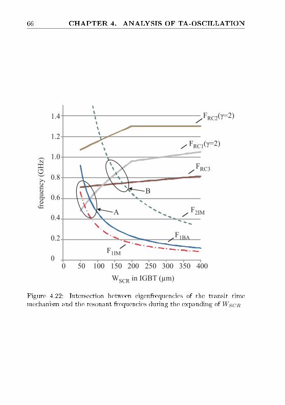
66 CHAPTER 4. ANALYSIS OF TA-OSCILLATION
0
0.2
0.4
0.6
0.8
1.0
1.2
1.4
0 50 100 150 200 250 300 350 400
FRC3
F ( =2)RC1 γ
F ( =2)RC2 γ
F1IM
F2IM
F1BA
W in IGBT (µm)SCR
freq
uen
cy (
GH
z)
A
B
Figure 4.22: Intersection between eigenfrequencies of the transit timemechanism and the resonant frequencies during the expanding of WSCR
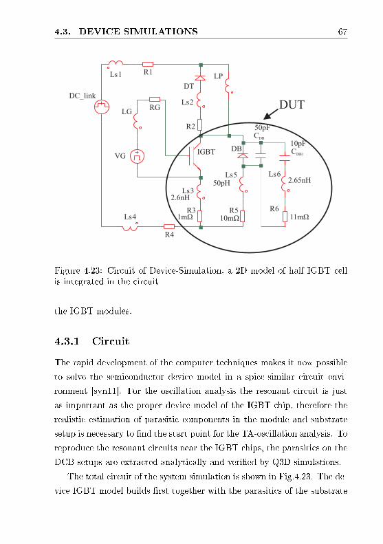
4.3. DEVICE SIMULATIONS 67
DT
VG
LG
LP
IGBT
DUT
Ls1
DC_linkLs2
R1
R2
R5
Ls5
Ls3
R3
R4
Ls4
RG
DB CDB1
R6
Ls6
11mΩ10mΩ1mΩ
2.6nH
50pH 2.65nH
10pF
50pFCDB
Figure 4.23: Circuit of Device-Simulation, a 2D model of half IGBT cellis integrated in the circuit
the IGBT modules.
4.3.1 Circuit
The rapid development of the computer techniques makes it now possible
to solve the semiconductor device model in a spice-similar circuit envi-
ronment [syn11]. For the oscillation analysis the resonant circuit is just
as important as the proper device model of the IGBT chip, therefore the
realistic estimation of parasitic components in the module and substrate
setup is necessary to nd the start point for the TA-oscillation analysis. To
reproduce the resonant circuits near the IGBT chips, the parasitics on the
DCB setups are extracted analytically and veried by Q3D simulations.
The total circuit of the system simulation is shown in Fig.4.23. The de-
vice IGBT model builds rst together with the parasitics of the substrate
68 CHAPTER 4. ANALYSIS OF TA-OSCILLATION
setups a single IGBT switch (DUT), which consists of three resonant cir-
cuits as shown in Fig.4.19. Ls3 and R3 together with Ls5 and R5 represent
the wire bonding between the IGBT and the diode, and the Ls6 and R6
represent the wire bonding between the diode and the copper area on the
top of the DCB. The series switching of CCB and CEB is simplied as
CDB1. And CDB represents the junction capacitance of the diode DB.
The DUT is again integrated in the test circuit corresponding to labour
setup for the measurement. The entire test process is solved by Sentaurus
device simulator. In contrast to the previous HF-oscillation simulations,
the turn-o process is simulated without articial HF-stimulations. The
maximal time step during the IGBT turning-o is limited to 0.2ns, which
is found to be a good compromise between the simulation time and the
convergence. The time derivative of the current signal on R5 represents
the antenna signal in the measurement.
Oscillations are observed on the current of R5 during the whole ramp up
process of VCE . The frequencies of the weak oscillation decrease according
to the extension of the SCR from 560MHz to 200MHz before the strong
oscillation occurs. At the time of MOS-channel turned-o, the strong
oscillation occurs with the frequency of around 600Mhz. Oscillations with
similar frequency trend can also be observed on the ne resolved VCE and
ICE .
4.3.2 Eect of resonant circuit's eigenfrequencies
The varying of CDB1 shows a signicant eect on the oscillation signals.
The frequencies of the oscillations reduce according to the increase of
CDB1. The maximal amplitude is found at 610MHz and CDB1=22pF
as shown in Fig.4.25(a). The circuit congurations of the device simu-
lation are analysed by network simulation parallel to the device simula-
tion. As the network simulator does not solve the semiconductor equa-
tions, the parameters such capacitance and inductance of the semiconduc-
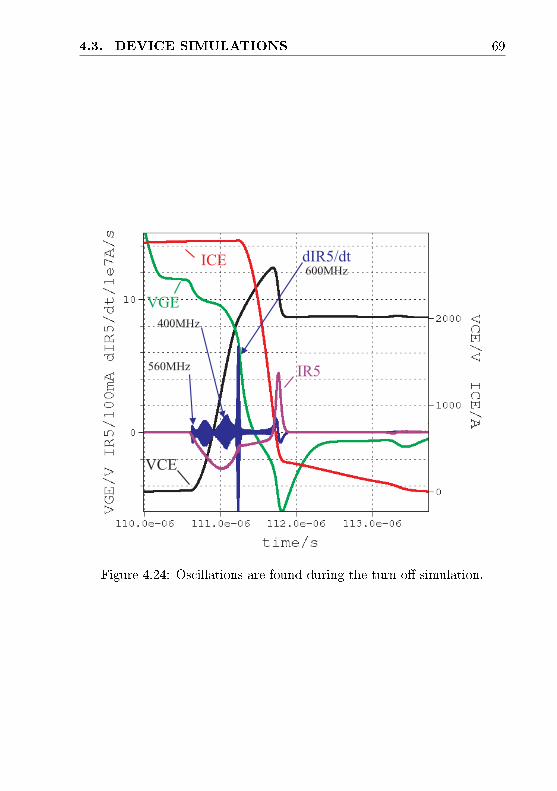
4.3. DEVICE SIMULATIONS 69
600MHz
400MHz
560MHzIR5
dIR5/dtICE
VCE
VGE
Figure 4.24: Oscillations are found during the turn-o simulation.
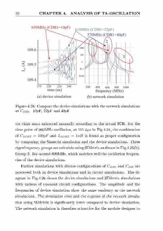
70 CHAPTER 4. ANALYSIS OF TA-OSCILLATION
frequency (MHz)200
0.01
0.1
1
10
100
21
3
650MHz (CDB1=10pF)610MHz (CDB1=22pF)
570MHz (CDB1=40pF)
(a) device simulation (b) network simulation
I(A
)C
E
109.6
109.5
109.4
400 600 800 1000210 220 230 240
time (ns)
Figure 4.25: Compare the device simulations with the network simulationsat CDB1=10pF, 22pF and 40pF
tor chips must extracted manually according to the actual SCR. For the
time point of 600MHz oscillation, at 111.2µs in Fig.4.24, the combination
of CIGBT = 100pF and LIGBT = 1nH is found as proper conguration
by comparing the Simetrix simulation and the device simulations. Three
eigenfrequency groups are calculate using SIMetrix as shown in Fig.4.25(b).
Group 2. lies around 600MHz, which matches well the oscillation frequen-
cies of the device simulations.
Further simulations with diverse congurations of CDB1 and CDB are
processed both in device simulations and in circuit simulations. The di-
agram in Fig.4.26 shows the device simulations and SIMetrix simulations
with various of resonant circuit congurations. The amplitude and the
frequencies of device simulation show the same tendency as the network
simulations. The simulation time and the expense of the network simula-
tion using SIMetrix is signicantly lower compared to device simulation.
The network simulation is therefore attractive for the module designer to
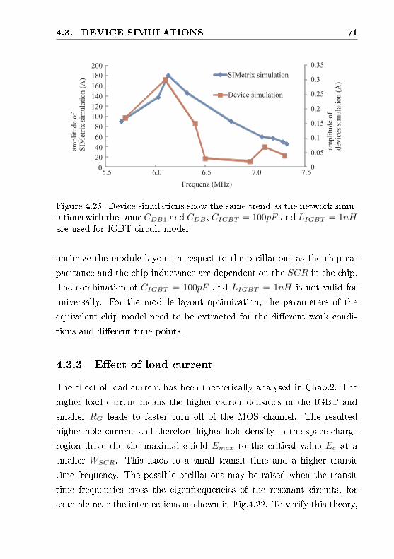
4.3. DEVICE SIMULATIONS 71
0
0.05
0.1
0.15
0.2
0.25
0.3
0.35
0
20
40
60
80
100
120
140
160
180
200
5.5 6.0 6.5 7.0 7.5
Frequenz (MHz)
SIMetrix simulation
Device simulation
amp
litu
de
of
SIM
etri
x s
imu
lati
on
(A
)
amp
litu
de
of
dev
ices
sim
ula
tio
n (
A)
Figure 4.26: Device simulations show the same trend as the network simu-lations with the same CDB1 and CDB , CIGBT = 100pF and LIGBT = 1nHare used for IGBT circuit model
optimize the module layout in respect to the oscillations as the chip ca-
pacitance and the chip inductance are dependent on the SCR in the chip.
The combination of CIGBT = 100pF and LIGBT = 1nH is not valid for
universally. For the module layout optimization, the parameters of the
equivalent chip model need to be extracted for the dierent work condi-
tions and dierent time points.
4.3.3 Eect of load current
The eect of load current has been theoretically analysed in Chap.2. The
higher load current means the higher carrier densities in the IGBT and
smaller RG leads to faster turn o of the MOS channel. The resulted
higher hole current and therefore higher hole density in the space charge
region drive the the maximal e-eld Emax to the critical value Ec at a
smaller WSCR. This leads to a small transit time and a higher transit
time frequency. The possible oscillations may be raised when the transit
time frequencies cross the eigenfrequencies of the resonant circuits, for
example near the intersections as shown in Fig.4.22. To verify this theory,
72 CHAPTER 4. ANALYSIS OF TA-OSCILLATION
the load current IL is varied from 18 A/cm2 to 181 A/cm2.
The oscillation peak is rst found at 56Acm2 with the frequency of
400Mhz, then reduces with the increasing IL and then reaches its second
peak amplitude at 109Acm2 with the frequency of 650MHz. Fig.4.28 shows
the expansion of SCR in the IGBT device model at the moment of the os-
cillations. The oscillation frequencies of the device simulation match well
with the measurements. For IL = 56A, WSCR = 155µm as the 400Mhz
oscillation happens. For IL = 109A, WSCR = 205µm as the 650MHz
oscillation happens. The eigenfrequencies of the resonant circuit can be
read out in Fig.4.22 with indications of work points group A for 400MHz
and work points group B for 650MHz oscillations according to the current
WSCR. During the trun-o, the expanding of SCR leads to the decrease
of transit time frequencies of IGBT and increase of the resonance frequen-
cies on the substrate. The transit time frequencies match the resonance
frequencies rst time at around 400MHz near the work points group A in
Fig.4.22. As the dynamic avalanche does not occure, the 400MHz oscil-
lation is induced mainly by PETT mechanisms. The further expanding
of the SCR leads temporarily to the mismatch between the transit time
frequencies and the resonance frequencies and decay of the oscillation. For
IL = 109A, as the SCR expands to about 200µm, the dynamic avalanche
happens. The transit time frequencies match the resonance frequencies
at 650MHz near the work points group B in Fig.4.22. The frequencies
of the simulated oscillations are lower than the analytical estimated fre-
quencies. The possible reason for the deviations between the oscillation
frequencies and the estimated resonant frequencies is the time-delay of the
avalanche region in IGBT, which is not involved in the simplied resonant
circuit model in Fig.4.19. The equivalent circuit of the avalanche region
for microwave diode has been derived analytically by Gilden and Hines
[GH66]. Although the avalanche region can be described by the parallel
switching of a inductance La and a capacitance Ca, but they are strong
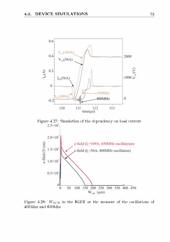
4.3. DEVICE SIMULATIONS 73
time(µs)110 111 112 113
I(A
)R
5
-0.2
0
0.2
0.4
0.6
V/(
V)
CE
0
1000
2000VCE(109A)
650Mhz
400MHz
VCE(56A)
IR5(109A)
IR5(56A)
Figure 4.27: Simulation of the dependency on load current
0
0.5×10⁵
1.0×10⁵
1.5×10⁵
2.0×10⁵
2.5×10⁵
0 50 100 150 200 250 300 350 400 450
e-field (I =109A, 650MHz oscillatzion)L
e-field (I =56A, 400MHz oscillation)L
e-fi
led (
V/c
m)
W (µm)CSR
Figure 4.28: WSCR in the IGBT at the moment of the oscillations of400Mhz and 650Mhz
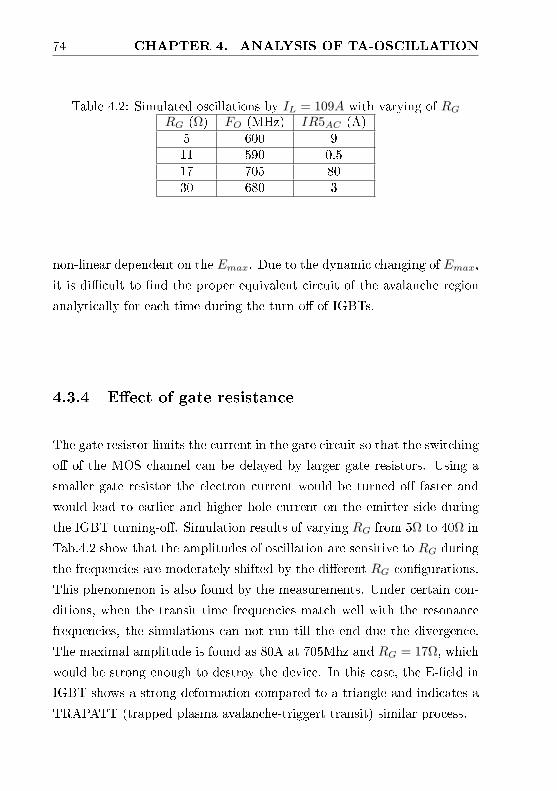
74 CHAPTER 4. ANALYSIS OF TA-OSCILLATION
Table 4.2: Simulated oscillations by IL = 109A with varying of RG
RG (Ω) FO (MHz) IR5AC (A)5 600 911 590 0.517 705 8030 680 3
non-linear dependent on the Emax. Due to the dynamic changing of Emax,
it is dicult to nd the proper equivalent circuit of the avalanche region
analytically for each time during the turn o of IGBTs.
4.3.4 Eect of gate resistance
The gate resistor limits the current in the gate circuit so that the switching
o of the MOS channel can be delayed by larger gate resistors. Using a
smaller gate resistor the electron current would be turned o faster and
would lead to earlier and higher hole current on the emitter side during
the IGBT turning-o. Simulation results of varying RG from 5Ω to 40Ω in
Tab.4.2 show that the amplitudes of oscillation are sensitive to RG during
the frequencies are moderately shifted by the dierent RG congurations.
This phenomenon is also found by the measurements. Under certain con-
ditions, when the transit time frequencies match well with the resonance
frequencies, the simulations can not run till the end due the divergence.
The maximal amplitude is found as 80A at 705Mhz and RG = 17Ω, which
would be strong enough to destroy the device. In this case, the E-eld in
IGBT shows a strong deformation compared to a triangle and indicates a
TRAPATT (trapped plasma avalanche-triggert transit) similar process.
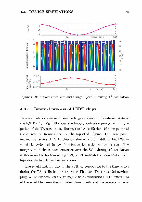
4.3. DEVICE SIMULATIONS 75
I(A
)R
5
time(ns)241 242
1×10²⁰
2×10²⁰
3×10²⁰
Inte
gr_
Imp
act
1/(
cm^2
×s)
time(ns)241 242
-4
-2
0
Y(µ
m)
40
50
60
01
02
03
0
Imp
actI
on
izat
ion
1/(
s×cm
)-3
1×
10
23
5×
10
22
1×
10
22
Figure 4.29: Impact ionization and charge injection during TA-oscillation
4.3.5 Internal process of IGBT chips
Device simulations make it possible to get a view on the internal state of
the IGBT chip. Fig.4.29 shows the impact ionization process within one
period of the TA-oscillation. During the TA-oscillation, 10 time points of
the current in R5 are shown on the top of the gure. The correspond-
ing internal states of IGBT chip are shown in the middle of Fig.4.29, in
which the periodical change of the impact ionization can be observed. The
integration of the impact ionization over the SCR during TA-oscillation
is shown on the bottom of Fig.4.29, which indicates a periodical current
injection during the avalanche process.
The e-eld distributions in the SCR, corresponding to the time points
during the TA-oscillation, are shown in Fig.4.30. The sinusoidal overlap-
ping can be observed on the triangle e-eld distributions. The dierences
of the e-eld between the individual time points and the average value of
76 CHAPTER 4. ANALYSIS OF TA-OSCILLATION
one oscillation period are dened as Eq.(4.9). In Fig.4.31 a propagating
wave of ∆E(x, n) is clearly visible. As shown in Fig.4.32 and Fig.4.33,
the propagating waves are also observed on the electron distribution and
hole distribution in the SCR. The wave is induced by the drift of electrons
packet from emitter side to collector side with the velocities of 8.56cm/s.
And the wave of holes spreads in the reverse direction with the velocity of
7.75cm/s. The velocities comply with the eective saturation velocities of
electrons packet and holes packet in the SCR respectively. The variation
of the eDensity in the SCR is much stronger than that of the hDensity,
which indicates the dominant roll of the electron transit time eect in the
TA-oscillation.
∆E(x, n) = E(x, n)− E(x, n);n = 1, 2, . . . , 11 (4.9)
∆eDensity(x, n) = eDensity(x, n)− eDensity(x, n);n = 1, 2, . . . , 11
(4.10)
∆hDensity(x, n) = hDensity(x, n)− hDensity(x, n);n = 1, 2, . . . , 11
(4.11)
4.3.6 Eect of impact ionization
The exibility of device Simulation allows to answer the question, if the
TA-oscillation is solely caused by the avalanche. After that the oscillation
of 600Mhz is reproduced by the reference simulation, the simulation is
repeated with deactivated impact ionization. Although it is not possible
to turn o the impact ionization in real IGBT chips, this comparison is
the simple method to verify, if the TA-oscillation is solely caused by the
impact ionization. Fig.4.34 shows two simulations with identical parameter
settings except of the impact Ionization. On the top left is the turn-
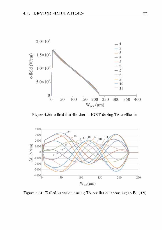
4.3. DEVICE SIMULATIONS 77
0 50 100 150 200 250 300 350 4000
5.0×10⁴
1.0×10⁵
1.5×10⁵
2.0×10⁵
e-fi
eld (
V/c
m)
W (µm)SCR
t1
t2
t3
t4
t5
t6
t7
t8
t9
t10
t11
Figure 4.30: e-eld distribution in IGBT during TA-oscillation
-4000
-3000
-2000
-1000
0
1000
2000
3000
4000
t1
t2
t3
t4
t5
t6t7 t8 t9
t10t11
0 50 100 150 200 250
W (µm)SCR
DE
(V
/cm
)
Figure 4.31: E-led variation during TA-oscillation according to Eq.(4.9)
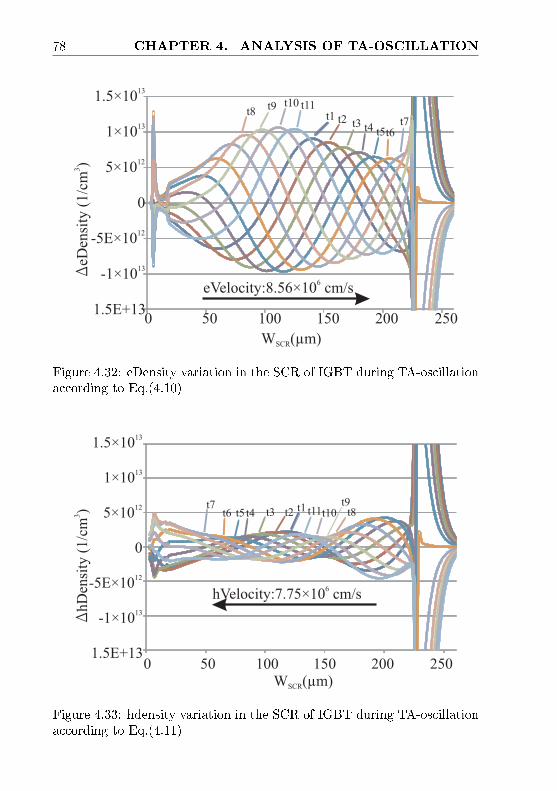
78 CHAPTER 4. ANALYSIS OF TA-OSCILLATION
W (µm)SCR
DeD
ensi
ty (
1/c
m )3
1.5E+13
-1×10¹³
-5E×1012
0
5×10¹²
1×10¹³
1.5×10¹³
0 50 100 150 200 250
eVelocity:8.56×10 cm/s6
t2 t3 t4 t5t6t7
t8t9 t10 t11
t1
Figure 4.32: eDensity variation in the SCR of IGBT during TA-oscillationaccording to Eq.(4.10)
DhD
ensi
ty (
1/c
m )3
W (µm)SCR
0 50 100 150 200 250
hVelocity:7.75×10 cm/s6
1.5E+13
-1×10¹³
-5E×1012
0
5×10¹²
1×10¹³
1.5×10¹³
t2t3t4t5t6t7
t8t9
t10t11t1
Figure 4.33: hdensity variation in the SCR of IGBT during TA-oscillationaccording to Eq.(4.11)
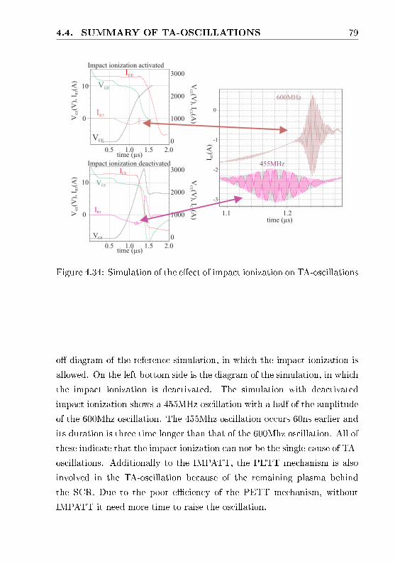
4.4. SUMMARY OF TA-OSCILLATIONS 79
0
10
0
IR5
VCE
ICE
VGE
time (µs)0.5 1.0 1.5 2.0
V(V
), I
(A)
GE
R5
0
10
V(V
), I(A
)C
EC
E
0
1000
2000
3000ICE
VGE
VCE
IR5
time (µs)0.5 1.0 1.5 2.0
V(V
), I
(A)
GE
R5
0
10
V(V
), I(A
)C
EC
E
0
1000
2000
3000
Impact ionization activated
Impact ionization deactivated
0
-1
-2
-3
time (µs)1.1 1.2
I(A
)R
5
600MHz
455MHz
Figure 4.34: Simulation of the eect of impact ionization on TA-oscillations
o diagram of the reference simulation, in which the impact ionization is
allowed. On the left bottom side is the diagram of the simulation, in which
the impact ionization is deactivated. The simulation with deactivated
impact ionization shows a 455MHz oscillation with a half of the amplitude
of the 600Mhz oscillation. The 455Mhz oscillation occurs 60ns earlier and
its duration is three time longer than that of the 600Mhz oscillation. All of
these indicate that the impact ionization can not be the single cause of TA-
oscillations. Additionally to the IMPATT, the PETT mechanism is also
involved in the TA-oscillation because of the remaining plasma behind
the SCR. Due to the poor eciency of the PETT mechanism, without
IMPATT it need more time to raise the oscillation.
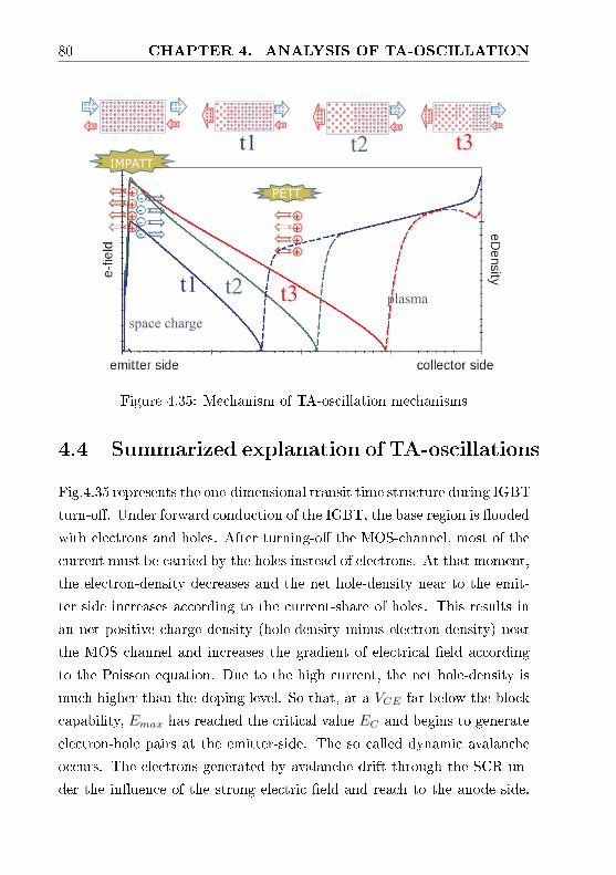
80 CHAPTER 4. ANALYSIS OF TA-OSCILLATION
t1
-
-
-
-
-
-
-
-
-
-
-
-
-
-
-
-
-
-
-
-
-
-
-
-
-
-
-
-
-
-
-
-
-
-
-
-
-
-
-
-
-
-
-
-
-
-
-
-
-
-
-
-
-
-
-
-
-
-
-
-
-
-
-
-
-
- -
- -
-
-
- -
- -
-
-
-
-
-
-
-
-
-
-
-
-
-
-
-
-
-
-
-
-
-
-
-
-
-
-
-
-
-
-
-
-
-
-
-
-
-
-
-
-
-
-
-
-
-
-
-
-
-
-
-
-
-
-
- -
- -
-
-
-
-
-
-
-
-
-
-
-
-
-
-
-
-
-
-
-
-
-
-
-
-
-
-
-
-
-
-
-
-
-
-
-
-
-
-
- -
- -
-
-
--
-
-
-
-
-
-
-
-
-
-
-
-
-
-
-
-
-
-
-
-
-
-
-
-
-
-
- -
- -
-
IMPATT
PETT+-
+-
+-
+-
+
+
+
+
space charge
plasmat1 t2 t3
t2 t3
Figure 4.35: Mechanism of TA-oscillation mechanisms
4.4 Summarized explanation of TA-oscillations
Fig.4.35 represents the one-dimensional transit time structure during IGBT
turn-o. Under forward conduction of the IGBT, the base region is ooded
with electrons and holes. After turning-o the MOS-channel, most of the
current must be carried by the holes instead of electrons. At that moment,
the electron-density decreases and the net hole-density near to the emit-
ter side increases according to the current-share of holes. This results in
an net positive charge density (hole-density minus electron-density) near
the MOS channel and increases the gradient of electrical eld according
to the Poisson equation. Due to the high current, the net hole-density is
much higher than the doping level. So that, at a VCE far below the block
capability, Emax has reached the critical value EC and begins to generate
electron-hole pairs at the emitter-side. The so called dynamic avalanche
occurs. The electrons generated by avalanche drift through the SCR un-
der the inuence of the strong electric eld and reach to the anode side.
4.4. SUMMARY OF TA-OSCILLATIONS 81
Similar to the IMPATT mechanism the transit-time eect hereby gives an
oscillation trend to the IGBT chip. The injection-time together with the
transit-time of the holes induces a phase shift between the terminal voltage
and terminal current in RF-range. At certain frequencies, the IGBT can
act as an amplier. When the addressable resonant circuits are present,
oscillations would be raised. Due to the high current, the plasma in the
base region is quickly extracted and the SCR is expanding fast to the
collector. The expanding of the SCR during the turn-o process disperses
the corresponding frequencies of the transit time structure from single fre-
quencies to a continuous frequency band depending on the actual width of
the depletion region (WSCR).
The parasitic components in IGBT modules, for example stray induc-
tance of bond wires and junction capacitance of the free wheel diode can
together with the IGBT chip build up resonance circuits. The exten-
sion of SCR leads to on one hand the longer transit time of the carri-
ers, on the other hand leads to the reduction of the chip capacitance and
therefore the higher eigenfrequencies of the according resonant circuits. If
the eigenfrequencies of such resonance circuits match the frequency of the
transient-time eect, the Transient Avalanche Oscillation would be raised.
Oscillations would occur around the intersections of the eigenfrequencies
of the resonant circuit and the eciency of the amplier being high.
TA-oscillations are successfully reproduced by device simulations using
a two dimension IGBT model which is integrated in a resonant circuit sim-
ilar to the module setups. Eigenfrequency of the resonant circuit ts the
second maximum of IMPATT eciency resulting in an oscillation around
600MHz. The internal semiconductor states show that the e-eld and carri-
ers distributions in the space charge region are overlapped by space waves.
The velocities of the waves are appropriate to the corresponding carrier ve-
locities. The IMPATT mechanism is the key player in the TA-oscillation.
And additionally, the remaining plasma behind the SCR allows also for
82 CHAPTER 4. ANALYSIS OF TA-OSCILLATION
the plasma extraction transition time (BARITT/PETT) mechanism.
Although TA-oscillations can be raised theoretically at each voltage
class of IGBTs. TA-oscillations are until now only observed by IGBTs
with over 3.3kV blocking voltage. The device simulations in this work are
based on a 2D half IGBT cell. The lament eects due to the current com-
mutation between the adjacent cell and the paralleled chips can therefore
not be investigated.
Chapter 5
Countermeasures to
Transient Avalanche
oscillations
5.1 Essential measures
to suppress TA-oscillations
According to the measurements and analysis in the previous chapters, the
dynamic avalanche generation and the transit time eect of the avalanche
electrons are identied as the root cause of the TA-oscillation. The high
load current density and the switching o of the electron current from the
MOS-channel are the key character of the turn o process, in which TA-
oscillation occurs. The corresponding general possible measures to avoid
the TA-oscillations can be summarised as following:
To apply limitation to the load current and the DC-link voltage so
that the dynamic avalanche does not occur.
84 CHAPTER 5. COUNTERMEASURES
To keep the gate resistor out of the range, in which the TA-oscillation
would be raised.
To avoid the high over voltage by low inductive module design so as
to suppress the dynamic avalanche process. This is because that the
large stray inductance in the current commutation circuit leads to
high over voltage and thus has the similar eect on TA-oscillation as
the high DC-link voltage.
To increase the stray inductance in the resonant circuit for pushing
down the resonant frequencies so that they can not be addressed
by the transit time eect of the IGBT. Simply, longer emitter wire
bonds lead to lower frequency of TA-oscillations. But the high stray
inductance would lead to the high over voltage, that the aects the
module performance negatively.
For the investigated 3.3kV IGBT chip, the TA-oscillations can be
avoided by setting up the resonant circuits, so that the resonant fre-
quencies are out of the frequency range from 100MHz to 800MHz.
As the eigenfrequencies and the resonant frequencies change dynami-
cally during the turning o, it is dicult to mismatch the frequencies
all the turn-o time. The cross wire bonding between the adjacent
IGBTs is eective for the suppression of the low frequency oscillation
but not eective for the high frequency TA-oscillation.
To apply additional electron current from the channel, during the
time that TA-oscillation normally happens, is proved to be an ef-
fective method against the TA-oscillation. The absence of electrons
leads to the high e-eld peak near to the emitter side. When the
additional electron current is applied from the MOS channel to the
SCR, near to the emitter side the derivative dE/dX of the E-eld
could be reduced and therefore the peak value of the e-eld and
accordingly the avalanche generation is suppressed. The timing of
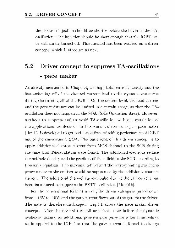
5.2. DRIVER CONCEPT 85
the electron injection should be shortly before the begin of the TA-
oscillation. The injection should be short enough that the IGBT can
be still surely turned o. This method has been realized on a driver
concept, which I introduce as next.
5.2 Driver concept to suppress TA-oscillations
- pace maker
As already mentioned in Chap.4.4, the high total current density and the
fast switching o of the channel current lead to the dynamic avalanche
during the turning o of the IGBT. On the system level, the load current
and the gate resistance can be limited in a certain range, so that the TA-
oscillation does not happen in the SOA (Safe Operation Area). However,
methods to suppress and to avoid TA-oscillation with out restriction of
the applications are desired. In this work a driver concept - pace maker
[Hon13] is developed to get oscillation free switching performance of IGBT
out of the conventional SOA. The basic idea of this driver concept is to
apply additional electron current from MOS channel to the SCR during
the time that TA-oscillation were found. The additional electrons reduce
the net hole density and the gradient of the e-eld in the SCR according to
Poisson's equation. The maximal e-eld and the corresponding avalanche
process near to the emitter would be suppressed by the additional channel
current. The additional channel current pulse during the tail current has
been introduced to suppress the PETT oscillation [Mou01b].
For the conventional IGBT turn o, the driver voltage is pulled down
from +15V to -15V, and the gate current ows out of the gate to the driver.
The gate is therefore discharged. Fig.5.1 shows the pace maker driver
concept. After the normal turn o and short time before the dynamic
avalanche occurs, an additional positive gate pulse for a few hundreds of
ns is applied to the IGBT so that the gate current is forced to change
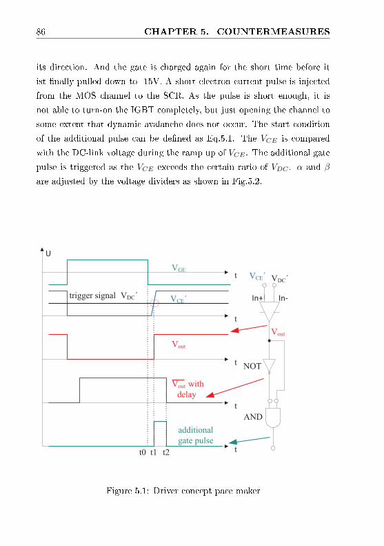
86 CHAPTER 5. COUNTERMEASURES
its direction. And the gate is charged again for the short time before it
ist nally pulled down to -15V. A short electron current pulse is injected
from the MOS channel to the SCR. As the pulse is short enough, it is
not able to turn-on the IGBT completely, but just opening the channel to
some extent that dynamic avalanche does not occur. The start condition
of the additional pulse can be dened as Eq.5.1. The VCE is compared
with the DC-link voltage during the ramp up of VCE . The additional gate
pulse is triggered as the VCE exceeds the certain ratio of VDC . α and β
are adjusted by the voltage dividers as shown in Fig.5.2.
t
t
t
t
t
U
t0 t1 t2
VGE
VCE´
additional
gate pulse
Vout with
delay
trigger signal VDC´ In-In+
AND
VCE´
Vout
Vout
VDC´
NOT
Figure 5.1: Driver concept pace maker
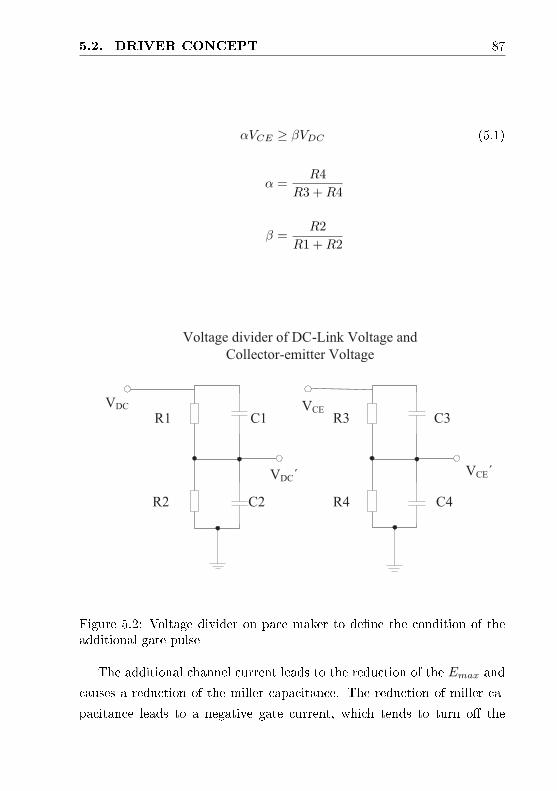
5.2. DRIVER CONCEPT 87
αVCE ≥ βVDC (5.1)
α =R4
R3 +R4
β =R2
R1 +R2
R1
R2
C1
C2
VDC´
R3
R4
C3
C4
VCE
VCE´
Voltage divider of DC-Link Voltage and
Collector-emitter Voltage
VDC
Figure 5.2: Voltage divider on pace maker to dene the condition of theadditional gate pulse
The additional channel current leads to the reduction of the Emax and
causes a reduction of the miller capacitance. The reduction of miller ca-
pacitance leads to a negative gate current, which tends to turn o the
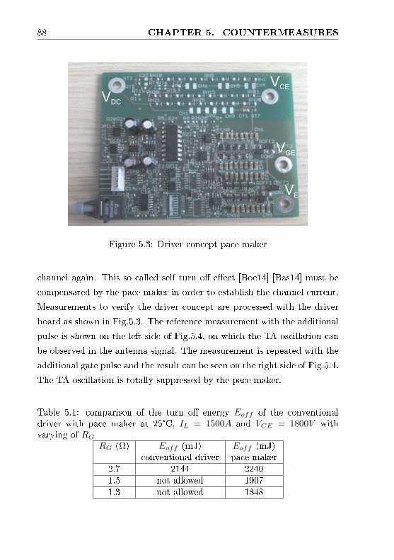
88 CHAPTER 5. COUNTERMEASURES
VCE
VDC
VE
VGE
Figure 5.3: Driver concept pace maker
channel again. This so called self turn o eect [Boe14] [Bas14] must be
compensated by the pace maker in order to establish the channel current.
Measurements to verify the driver concept are processed with the driver
board as shown in Fig.5.3. The reference measurement with the additional
pulse is shown on the left side of Fig.5.4, on which the TA-oscillation can
be observed in the antenna signal. The measurement is repeated with the
additional gate pulse and the result can be seen on the right side of Fig.5.4.
The TA-oscillation is totally suppressed by the pace maker.
Table 5.1: comparison of the turn o energy Eoff of the conventionaldriver with pace maker at 25°C, IL = 1500A and VCE = 1800V withvarying of RG
RG (Ω) Eoff (mJ) Eoff (mJ)conventional driver pace maker
2.7 2144 22401.5 not allowed 19071.3 not allowed 1848
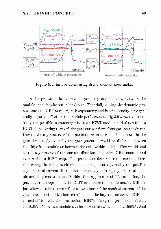
5.2. DRIVER CONCEPT 89
400ns/div
V =0GE
V =0antenna
V =0CE
I =0CE
Vantenna:2V/div
VGE: 5V/div
ICE : 1000A/div
VCE: 500V/div
Vantenna:2V/div
VGE: 5V/div
ICE : 1000A/div
VCE: 500V/div
V =0GE
V
=0antenna
V =0CE
I =0CE
turn-off without pacemaker turn-off with pacemaker
400ns/div
Figure 5.4: Improvement using driver concept pace maker
In the practice, the essential asymmetry and inhomogeneity in the
module- and chip-layout is inevitable. Especially during the dynamic pro-
cess, such as IGBT turn o, such asymmetry and inhomogeneity have gen-
erally negative eect on the module performance. Fig.5.5 shows schemat-
ically the possible asymmetry within an IGBT module and also within a
IGBT chip. During turn o, the gate current ows from gate to the driver.
Due to the asymmetry of the parasitic resistance and inductance in the
gate circuits, dynamically the gate potential would be dierent between
the chips in a module or between the cells within a chip. This would lead
to the asymmetry of the current distribution in the IGBT module and
even within a IGBT chip. The pacemaker driver forces a current direc-
tion change in the gate circuit. This compensates partially the possible
asymmetrical current distribution due to any existing asymmetrical mod-
ule and chip construction. Besides the suppression of TA-oscillation, the
pacemaker concept makes the IGBT even more robust. Generally IGBT is
just allowed to be turned o up to two times of the nominal current. If the
ICE exceeds this limit, short circuit should be imposed before the IGBT is
turned o to avoid the destruction [HB97]. Using the pace maker driver,
the 3.3kV 1500A test module can be successful switched o at 5000A. And
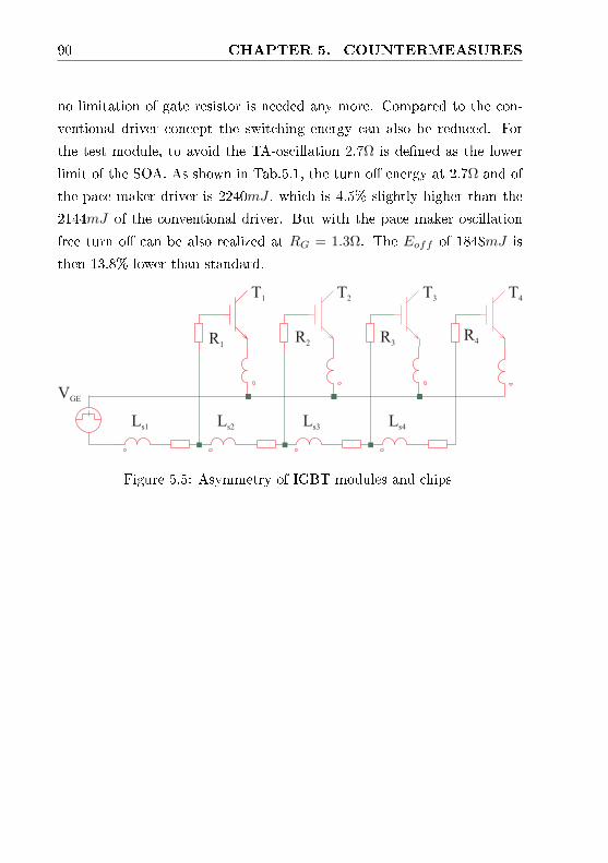
90 CHAPTER 5. COUNTERMEASURES
no limitation of gate resistor is needed any more. Compared to the con-
ventional driver concept the switching energy can also be reduced. For
the test module, to avoid the TA-oscillation 2.7Ω is dened as the lower
limit of the SOA. As shown in Tab.5.1, the turn o energy at 2.7Ω and of
the pace maker driver is 2240mJ , which is 4.5% slightly higher than the
2144mJ of the conventional driver. But with the pace maker oscillation
free turn o can be also realized at RG = 1.3Ω. The Eoff of 1848mJ is
then 13.8% lower than standard.
Ls1
R4R
3R
2R1
T4
T3
T2
T1
Ls2
Ls3
Ls4
VGE
Figure 5.5: Asymmetry of IGBT modules and chips
Chapter 6
Summary and outlook
6.1 Summary
Additionally to the PETT oscillation [GMS02] and dynamic IMPATT
[LSG98] oscillation, TA-oscillation is found to be a new type HF-oscillation
in IGBT modules. TA-oscillations are observed during the raising of the
collector voltage and the falling of the collector current, as the dynamic
avalanche is ongoing. TA-oscillation is much more dynamic compared to
the PETT oscillation and dynamic IMPATT oscillation in diode. The mea-
surements in this thesis show that the gate resistance, the DC-link voltage
and the load current are the essential parameter for the TA-oscillation.
Although the TA-oscillation is rst observed on the gate voltage trace,
no active participation of gate can be demonstrated. The HF-oscillation
signal on the gate trace is caused by HF-current in the emitter wire bond-
ing through electromagnetic coupling. The TA-oscillation appears just in a
certain range of gate resistor while the product of load current and DC-link
voltage is signicant of set of TA-oscillation, that indicates the correlation
of the TA-oscillation to the maximal e-eld of the space charge region
according to Eq.2.13. And the frequency of the TA-oscillation is found
92 CHAPTER 6. SUMMARY AND OUTLOOK
between 100 and 800Mhz, that indicates the eect from carrier transit
time.
The explanation of the TA-oscillation can be expressed as follows:
Under forward conduction of the IGBT, the base region is ooded with
electrons and holes. Due to turn o of the channel, the total load current
must be carried by holes. A space charge layer is building up on the emitter
side. Due to the high current, the net hole-density is much higher than
the doping level. Thus, dynamic avalanche occurs at collector voltage
far below the static blocking voltage of the IGBT. Electrons generated
by avalanche drift through the space charge region to the collector side
similar to the IMPATT diode. The transit time eect causes the chip
to act as a high-frequency amplier. Additionally, the remaining plasma
behind the collector side allows also for the plasma extraction transition
time (BARITT/PETT) mechanism.
The carrier injection time and the transit time lead to the phase shift
between the terminal HF-voltage and the HF-current. According to the
conventional consideration, for the IMPATT diode the maximal HF-power
generation occurs at the transit angle of π for IMPATT diode and 3/2π
for the BARITT diode [Sze81] [EH98]. Till now such consideration is also
applied to the frequency estimation of PETT oscillation and dynamic IM-
PATT oscillations [GMS02] [LSG98] [MD10] [Hee14]. And no considera-
tion are taken for the transit angle above 2π. With this theory, for a 200µm
SCR the transit time frequency can be estimated as around 170MHz for
IMPATT and 240MHz for PETT/ BARITT mechanisms. This is much
lower than the measured oscillation frequencies in this thesis, i.e. 650MHz.
As the the power semiconductor chip thickness is not optimized for the RF-
power generation, the none ideal situation should also be considered. For
the understanding of the amplier mechanism, the analytical estimation
of the HF-energy conversion eciency of transit time diode of [EH98] is
extended in this thesis. The analysis in Chap.3 shows that additional to
6.1. SUMMARY 93
the optimal transit angle, RF-power generation is also quite possible at
the transit angle about 2.9π for IMPATT mechanism. Compared with
the conventional consideration that corresponds to three times higher IM-
PATT frequency. The frequency for maximal power generation eciency
is reversely proportional to the width of the space charge region. The ex-
panding of the SCR during turning o of IGBT leads to decreasing of the
transit time frequencies. Not only the amplication but also the resonant
circuit varies with the expanding of the space charge region. In the IGBT
module the resonant circuit is formed out of chip and substrate capacitance
as well as the inductance of the wire bonds from IGBT to the diode and
diode to the substrate. The diode capacitance is also part of the resonant
circuit. The chip capacitance is reversely proportional to the width of the
space charge region. During the turning o, the eigenfrequencies of the
resonant circuit rise with the expansion of the space charge region. Os-
cillations would occur around the intersections of the eigenfrequencies of
the resonant circuit and the transit time frequencies, that the eciency of
the amplier being high. Eigenfrequency of the resonant circuit ts with
the second maximum of IMPATT eciency and results in an oscillation
around 600MHz.
To reproduce the TA-oscillation, A two dimensional device model of
3.3kV trench eld stop IGBT was setup and integrated in the resonant cir-
cuit similar to a IGBT module. The device model and the resonant circuit
was again integrated in the test circuit similar to the measurement setup.
In contrast to the PETT simulation, TA-oscillations are successfully re-
produced without articial stimulations. The inuence of the parameters,
such as load current, gate resistance and emitter wire bonds, are veried
by the device simulation. The impact ionization shows a periodical pro-
cess, according to the sine wave of the oscillation. The electrical eld has
a sinusoidal shape overlapping a triangle, determined by the space charge.
Similar wave forms are also found on the electron-distribution and hole-
94 CHAPTER 6. SUMMARY AND OUTLOOK
distribution in space Charge Region. IMPATT-like mechanism plays the
key role in the TA-oscillation. The simulation with deactivated impact
ionization shows that in addition to the IMPATT, the PETT mechanism
can be also involved in the TA-oscillation.
All the analysis shows that the temporary absence of the electron on the
emitter side causes the high E-eld peak on the emitter side and leads to
TA-oscillation. In this thesis, a driver concept "pace maker"is developed
to open the channel again during the time the TA-oscillation normally
happens. As the pulse is short enough, it is not able to turn-on the IGBT
completely, but just opening the channel to some extent that dynamic
avalanche does not occur. Supplying electron current during critical period
of time is veried to be a eective method to suppression of dynamic
avalanche and the TA-oscillation. The pace maker make the IGBT even
more robust because of the compensation of the possible asymmetry in the
IGBT module.
6.2 Outlook
The one dimension model is used to analyse the RF-power generation
eciency of IMPATT structures analytically. And a narrow avalanche
region assumed to inject charge carriers in to the SCR with a delay of π.
During the turn o process of IGBT, the E-eld distribution in the SCR
changes quickly and this assumption is not always in accordance with the
reality and leads to deviation between the frequency estimation and the
measurement. Theoretical work can done to develop the more suitable
analytical model of the avalanche region during the dynamic changing of
E-eld distribution. Although the avalanche generation and the electron
transit time dominants in TA-oscillation, transit time eect of holes is also
found. Further work can be done to investigate the interaction between
electrons and holes during TA-oscillations.
6.2. OUTLOOK 95
Further research work can be done on the module and chip design of
IGBT to improve the dynamic performance. Generally, there are always
inevitable asymmetry and inhomogeneities in the IGBT Module, IGBT
chip and also within a single cell of the chip. In the conventional design,
the IGBT cells are constructed to get a uniform characteristic. Accord-
ingly, the current should be distributed homogeneously. But in reality, a
small non-homogeneity and unbalance is unavoidable. And it is generally
known that, the slight unavoidable non-homogeneity between and within
the IGBT cells may lead to current laments during the turn o processes
of IGBTs [MD10]. This would happen especially under the avalanche con-
dition. The kink on the VCE trace in Fig.4.14 is a sign of current la-
ments. In the current laments the local current density can reach up to
ten times the average value. Such laments therefore enhance the tran-
sient avalanche dramatically, especially in IGBT for high voltage and high
current application, such transient avalanche in IGBTs can become strong
enough, so that TA-oscillation takes place and raises EMI problem. Re-
duction of the density of the current laments would lead to improved
utilization of the IGBT volume. This leads to the idea to reduce the cur-
rent lament by integration of controlled inhomogeneities into the IGBT
chip and into the single cell designs. Further research work can be sug-
gested as follows [Hon14]:
To investigate the IGBT chip design by arrangement of dierent
(more than two) types of cells within an IGBT chip.
Generally, on the IGBT chip there are large number of IGBT
cells with the same cell type implemented. Due to the unavoidable
manufacturing tolerances and the asymmetry of the cell arrangement
on the chip the switching behaviour of the cells may slightly dier
from each other. Since the distribution of such dierences cannot
be controlled, such minimal dierence can lead to strong current
laments. In an IGBT chip, cells can be implemented with dier-
96 CHAPTER 6. SUMMARY AND OUTLOOK
ent channel widths; dierent channel contacts, dierent cell shapes
and sizes as well as dierent doping levels. To generate the non-
homogeneity on IGBT chips by regular or irregular arrangement of
various of cell types. Non-homogeneity of the order of regular arrays
of various cells of irregular shapes. The target is to suppress the cur-
rent lament by chip design from the uncontrolled non-homogeneity
to a controlled non-homogeneity.
To investigate the IGBT cell design to integrate inhomogeneity to
the gate channel within a IGBT cell.
The lateral non-homogeneity can be realized by deformation of
trench gate oxide. Due to the inhomogeneous eld distribution in the
channel region, during turn-o and before complete channel pinch-
o, the channel current can be divided to several sub-streams. The
limitation of the current commutation between the adjacent region
with in the cell would suppress the stronger laments and thus the
followed avalanche at channel pinch-o.
The trench bottom can also be implemented as wave form or
step form, so that the charge commutation from the p-oat to the
channel region can be homogeneously divided. This would help to
suppress TA-oscillations. And there must be other constructions,
such as jagged structure, can be introduced to get such eects.
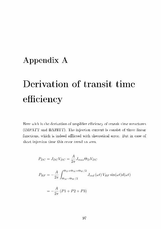
Appendix A
Derivation of transit time
eciency
Here with is the derivation of amplier eciency of transit time structures
(IMPATT and BARITT). The injection current is consist of three linear
functions, which is indeed aicted with theoretical error. But in case of
short injection time this error trend to zero.
PDC = JDCVDC =A
2πJmaxΘDVDC
PRF = − A
2π
∫ ΘD+ΘM+ΘW /2
ΘM−ΘW /2
Jind (ωt)VRF sin(ωt)d(ωt)
= − A
2π(P1 + P2 + P3)
97
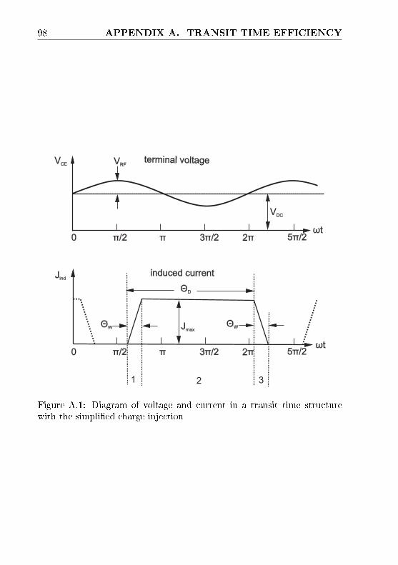
98 APPENDIX A. TRANSIT TIME EFFICIENCY
induced current
0 π 3π/2 2ππ/2
VRFVCE
VDC
ΘW
ΘD
ωt
ΘW
5π/2
Jind
Jmax
ωt
0 π 3π/2 2ππ/2 5π/2
terminal voltage
1 2 3
Figure A.1: Diagram of voltage and current in a transit time structurewith the simplied charge injection
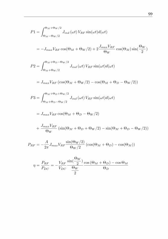
99
P1 =
∫ ΘM+ΘW /2
ΘM−ΘW /2
Jind (ωt)VRF sin(ωt)d(ωt)
= −JmaxVRF cos(ΘM +ΘW /2) + 2JmaxVRF
ΘWcos(ΘM ) sin(
ΘW
2)
P2 =
∫ ΘM+ΘD−ΘW /2
ΘM+ΘW /2
Jind (ωt)VRF sin(ωt)d(ωt)
= JmaxVRF (cos(ΘM +ΘW /2)− cos(ΘM +ΘD −ΘW /2))
P3 =
∫ ΘM+ΘD+ΘW /2
ΘM+ΘD−ΘW /2
Jind (ωt)VRF sin(ωt)d(ωt)
= JmaxVRF cos(ΘM +ΘD −ΘW /2)
+JmaxVRF
ΘW(sin(ΘM +ΘD +ΘW /2)− sin(ΘM +ΘD −ΘW /2))
PRF = − A
2πJmaxVRF
sin(ΘW /2)
ΘW /2(cos(ΘM +ΘD)− cos(ΘM ))
η =PRF
PDC= −VRF
VDC
sin(ΘW
2)
ΘW
2
cos (ΘM +ΘD)− cosΘM
ΘD
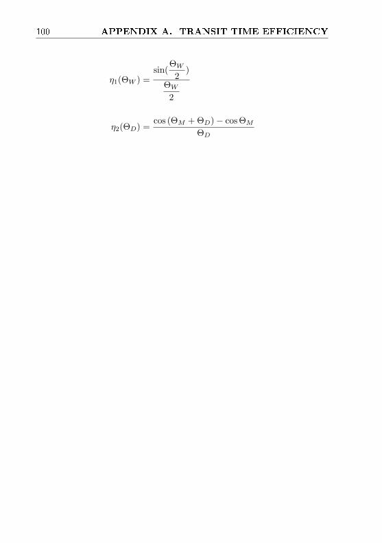
100 APPENDIX A. TRANSIT TIME EFFICIENCY
η1(ΘW ) =sin(
ΘW
2)
ΘW
2
η2(ΘD) =cos (ΘM +ΘD)− cosΘM
ΘD
Appendix B
Test box and the RF-noise
problems
At begin of the investigation on TA-oscillation, HF-disturbance at about
600MHz is some time observed on the trace of load current, as shown in
Fig.B.1. But the load current is measured by a Person coil, whose response
frequency is under 30MHz. The capacitive coupling in this case is respon-
sible for disturbance. Fig.B.2 shows the schematic of the test setup. The
impedance of the GND conductor between the test box and the oscillo-
scope, the impedance of the GND conductor of the BNC cabel between
Person current sense and the coupling capacitance of Persen current sense
to the test box built a closed loop, that capture the HF-oscillation signal
similarly to an antenna. The HF-signal measured at the oscilloscope is the
voltage drop on the BNC cable of the Person current sensor according to
the voltage divider as shown in Fig.B.2, but not the current signal. This
eect can be eliminated by enlarging the impedance of the GND conductor
between the test box and the oscilloscope.
101
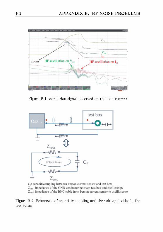
102 APPENDIX B. RF-NOISE PROBLEMS
zoom HF-oscillation on ICE
HF-oscillation on VGE
VGE
ICE
VCE
Figure B.1: oscillation signal observed on the load current
test box
Oszi .
HF EMV Störung
ZBNC
Zzero
CP
CP: capacitivecupling between Person current sensor and test box
Z : impedance of the GND conductor between test box and oscilloscope
Z : impedance of the BNC cable from Person current sensor to oscilloscopeGND
BNC
Figure B.2: Schematic of capacitive cupling and the voltage divider in thetest setup
Bibliography
[ABG+99] Auerbach, F. ; Bauer, J.G ;Glantschnig, M. ; Gottert,
J. ; Hierholzer, M. ; Porst, A. ; Reznik, D. ; Schulze,
H. ; Schulze, T. ; Spanke, R.: 6.5 kV IGBT-modules. In:
Industry Applications Conference 3 (1999), Nr. 34, S. 1770
1774
[Bal79] Baliga, B. J.: Enhancement and depletion mode veritcal
channel MOS gate thyristor. In: Electronic Letters 15 (1979),
September, Nr. 20, S. 645647
[Bas14] Basler, Thomas: Ruggedness of High-Voltage IGBTs and
Protection Solutions, Technische Universität ChemnitzUniver-
sity Bremen, Dissertation, 2014
[BD10] Bayerer, R. ; Domes, D.: Power circuit design for clean
switching. In: 6th IEEE International Conference on Inte-
grated Power Electronics Systems (CIPS) (2010), S. 16
[Boe14] Boehmer, Juergen W.: Wirkung des Ladungsträgerplasmas
auf das Abschaltenverhalten von Insulated Gate Bipolar Tran-
sistoren, University Rostock, Dissertation, Februar 2014
103
104 BIBLIOGRAPHY
[BS67] BENDA, HANSJOCHEN ; SPENKE, EBERHARD: Re-
verse recovery processes in silicon power rectiers. In: Pro-
ceedings of the IEEE 55 (1967), August, Nr. 8, S. 13311354
[BW80] Becke, Hans W. ; Wheathley, C. Frank J.: Power MOS-
FET with an anode region. In: U.S. patent No. 4,364,073
(1980), Nov.
[CMMO75] Canali, C. ;Majni, G. ;Minder, R. ; Ottaviani, G.: Elec-
tron and hole drift velocity measurements in silicon and their
empirical relation to electric eld and temperature. In: Elec-
tron Devices, IEEE Transactions 22 (1975), November, S.
1045 1047
[DLS03] Domeij, M. ; Lutz, J. ; Silber, D.: On the destruction
limit of Si power diodes during reverse recovery with dynamic
avalanche. In: IEEE TRANSACTIONS ON ELECTRON
DEVICES 50 (2003), Nr. 2, S. 486493
[EH98] Eisele, Heribert ; Harddad, George I.: Active microwave
diodes. In: Sze, SM (Hrsg.): Modern Semiconductor Device
Physics. New York : John Wiley & Sons, 1998, Kapitel 6, S.
343407
[FHK09] Fujita, Shigeto ; Hussein, Khalid H. ; Kitamura, Shuichi:
Investigation on IGBT High-Frequency Plasma. In: IEEE
TRANSACTIONS ON ELECTRON DEVICES 24 (2009),
Juni, Nr. 6, S. 15701576
[GH66] Gelden, M. ; Hines, E.: Electronic Tuning Eects in the
Read Microwave Avalanche Diode. In: IEEE TRANSAC-
TIONS ON ELECTRON DEVICES 13 (1966), Januar, Nr.
1, S. 169175
BIBLIOGRAPHY 105
[GMS01] Gutsmann, B. ; Mourick, P. ; Silber, D.: Hochfre-
quenzoszillationen im IGBT-Schweifstrom. In: Halbleiter-
Leistungsbauelemente und ihre systemtechnische Anwendung
(2001), Nr. 30
[GMS02] Gutsmann, B. ; Mourick, P. ; Silber, D.: Plasma ex-
traction transit time oscillations in bipolar power devices. In:
Solid State Electron. 46 (2002), April, Nr. 5, S. 133138
[Gut06] Gutsmann, Berndt: Charakterisierung und Einuss para-
sitrer elektromagnetischer Eekte in Leistungselektronischen
Systemen, University Bremen, Dissertation, August 2006
[HB97] Hierholze, M. ; Bayerer, R.: Improved Characteristics of
3.3kV IGBT Modules. In: PCIM (1997), Nr. 31. Nürnber
Germany
[Hee14] Heeb, Michael: Modellierung der parasitären passiven Ele-
mente in IGBT-Hochleistungsmodulen, University Kassel, Dis-
sertation, April 2014
[Hon13] Hong, T.: Ansteuerschaltung für Leistungshalbleiter. In:
Deutsche Patentanmeldung DE 10 2013 233 135 (2013), Nov.
[Hon14] Hong, T.: Inhomogenous Power Semiconductor De-
vices. In: United States Patent Application Publication
US20140131766A1 (2014), May
[HPB+14] Hong, T. ; Pfirsch, F. ; Bayerer, R. ; Lutz, J. ; Silber,
D.: Tansient Avalanche Ocillation of IGBTs Under high Cur-
rent ISPSD, 2014 (Proceedings of International Symposium
on Power Semiconductor Devices & IC's, Waikoloa, Hi 26), S.
355358
106 BIBLIOGRAPHY
[KOH+93] Kitagawa, M. ; Omura, I. ; Hasegawa, S. ; Inoue, T. ;
Nakagawa, A.: A 4500V Injektion enhanced Insulated gate
bipolar Transistor (IEGT) Operating in a Mode Similar to a
Thyristor. In: Electron Devices Meeting, 1993. IEDM '93.
Technical Digest., International (1993), S. 679682
[LMP+00] Laska, T. ; Münzer, M. ; Pfirsch, F. ; Schäffer, C. ;
Schmidt, T.: The Field Stop IGBT (FS IGBT). A new power
device concept with a great improvement potential. Toulouse,
Mai 2000 (Proceedings of International Symposium on Power
Semiconductor Devices & IC's 12), S. 355358
[LS94] Lutz, J. ; Scheuermann, U.: Advantages of the new con-
trolled axial lifetime diode. In: PCIM (1994), Nr. 28.
Nürnberg Germany
[LSG98] Lutz, J. ; Südkamp, W. ; Gerlach, W.: IMPATT os-
cillations in fast recovery diodes due to temporarily charged
radiation-induced deep levels. In: Solid-State Electronics 42
(1998), Juni, Nr. 6, S. 931938
[LSSD11] Lutz, Josef ; Schlangenotto, Heinrich ; Scheuermann,
Uwe ; Doncker, Rik D.: Semiconductor Power Devices. 1.
Springer Heiderberg Dordrecht London New York, 2011
[Lut00] Lutz, J.: Freilaufdiode für schnell schaltende Leistungsbauele-
mente, TU Ilmenau, Dissertation, 2000
[Lut06] Lutz, Josef: Halbleiter-Leistungsbauelemente. Berlin Heidel-
berg : Springer-Verlag, 2006
[MD10] Müller-Dauch, Andreas: Simulationsuntersuchungen zur
Grenzbelastbarkeit von IGBTs im Abschaltvorgang, University
Bremen, Dissertation, Dezember 2010
BIBLIOGRAPHY 107
[MGS02] Mourick, P. ; Gutsmann, B. ; Silber, D.: Ultra high
frequency oscillations in the reverse recovery current of fast
diodes. Santa FA NM, Juni 2002 (Proceedings of International
Symposium on Power Semiconductor Devices & IC's 14), S.
205208
[Mou01a] Mouick, P.: Method of driving power semiconductor mod-
ules. In: Deutsche Patentschrift DE10158374C1 (2001), Nov.
[Mou01b] Mouick, P.: Power semiconductor module control method
provides suppression of plasma extraction transit time os-
cillations using additional control pulse. In: Deutsche
PatentschriftDE10156618 C1 (2001), Nov.
[MRP05] Kap. 2.5 In: Martin R. Parker, William E. W.: The Elec-
tronics Handbool. CRC Pressp, 2005
[OFO99] Omura, I. ; Fichtner, W. ; Ohashi, H.: Oscillation Ef-
fects in IGBT's Related to Negative Capacitance Phenomena.
In: IEEE TRANSACTIONS ON ELECTRON DEVICES 46
(1999), Januar, Nr. 1, S. 237243
[OOSO97] Omura, I. ; Ogura, T. ; Sugiyama, K. ; Ohashi, H.: Carrier
injection enhancement eect of high voltage MOS devices- De-
vice physics and design concept. In: IEEE TRANSACTIONS
ON ELECTRON DEVICES (1997), Mai, S. 217220
[Pau81] Paul, Reinhold: Halbleitersonderbauelement Höchstfrquenz-
und Leistungsbauelemente. Berlin : VEB VERLAG TECH-
NIK, 1981 (Elektronische Festkörperbauelemente)
[P12] Pfirsch, F.: private communication 13.03.2012, Diss., 2012
108 BIBLIOGRAPHY
[R.B10] R.Bayerer: IGBT-driver circuit for desaturated turn-o
with high desaturation level. In: Patentschrift US 7768337
B2 (2010)
[RKK+02] Rahimo, M. ; Kopta, A. ; Kaminski, S. Eicherand N. ;
Bauer, F. ; Schlapbach, U. ; Linder, S.: Extending the
Boundary Limits of High Voltage IGBTs and diodes to above
8kV. In: International Symposium on Power Semiconductor
Devices & IC's (2002), Nr. 14, S. 4144
[Roe77] van de Roer, T.G.: D.C and small-signal A.C. propertiew
of Silicon BARITT diodes, University of Eindhoven, Disser-
tation, Januar 1977
[SGMM02] Silber, D. ; Gutsmann, B. ; Mourick, P. ; Miller, G.:
Semiconductor Component circuit with a reduced oscillation
tendency. In: Internationale Anmeldung WO 03/049185 A2
(2002), Nov.
[SGMM03] Silber, D. ; Gutsmann, B. ; Mourick, P. ; Miller, G.:
Halbleiterbauelementanordnung mit verminderter Oszillation-
sneigung. In: Deutsche Patentanmeldung DE 10159851 A1
(2003), Jun.
[Sho38] Shockley, William: Currents to Conductors Induced by
a Moving Point Charge. In: Journal of Applied Physics 9
(1938), Oktober, S. 635
[Sil05] Silbe, D.: Halbleiterbauelement, University Bremen, Vor-
lesungsskript, 2005
[Sil14] Silbe, D.: private communication 18.09.2014, Diss., 2014
[SL04] Siemieniec, R. ; Lutz, J.: Possibilities and limits of axial
lifetime control by radiation induced centres in fast recovery
BIBLIOGRAPHY 109
diodes. In: Microelectronics Journal 35 (2004), Nr. 3, S.
259267
[SLH04] Siemieniec, R. ; Lutz, J. ; Herzer, R.: Analysis of dy-
namic impatt oscillations caused by radiation induced deep
centers with local and homogenous vertical distribution. In:
IEE Proc.-Circuits Devices Syst. 151 (2004), Nr. 3, S. 219224
[SLNM03] Siemieniec, R. ; Lutz, J. ; Netzel, M. ;Maurick, P.: Tran-
sit time oscillations as a source of EMC problems in bipolar
power devices. In: EPE TRANSACTIONS ON ELECTRON
DEVICES (2003)
[SMNL06] Siemieniec, Ralf ; Mourick, Paul ; Netzel, Mario ; Lutz,
Josef: The Plasma Extraction Transit-Time Oscillation in
Bipolar Power Devices - Mechanism, EMC Eects, and Pre-
vention. In: IEEE TRANSACTIONS ON ELECTRON DE-
VICES 53 (2006), Februar, Nr. 2, S. 369379
[SN89] Schlangenotto, H. ; Neubrand, H.: Dynamischer
Avalanche beim Abschalten von GTO-Thyristoren und IG-
BTs. In: Arch. Elektrotechnik 72 (1989), S. 113
[SSL02a] Siemieniec, R. ; Südkamp, W. ; Lutz, J.: APPLYING DE-
VICE SIMULATION FOR LIFETIME-CONTROLLED DE-
VICES. In: Fourth IEEE International Caracas Conference
on Devices, Circuits and Systems, Aruba (2002)
[SSL02b] Siemieniec, R. ; Südkamp, W. ; Lutz, J.: Determination
of parameters of radiation induced traps in silicon. In: Solid-
State Electronicsl 46 (2002), Nr. 2, S. 891901
[syn11] synopsys: TCAD Sentaurus Version F-2011.09. 2011
110 BIBLIOGRAPHY
[Sze81] Sze, SM: Physics of Semiconductor Devices. 2. Edition. New
York : John Wiley & Sons, 1981
[TKY+98] Takahashi, Y. ; Koga, T. ; Yamasaki, K. ; Kirihata, H.
; Seki, Y. ; Eschrich, F.: 2.5kV/1800A Power Pack IGBT.
Bad Nauheim, Mai 1998 (ETG - Fachbericht 72), S. 4354
[TYK+97] Takahashi, Y. ; Yoshikawa, K. ; Koga, T. ; Soutome, M.
; Takano, T. ; Kirihata, H. ; Seki, Y.: Ultra high-power
2.5kV-1800A Power Pack IGBT. Weimar, Mai 1997 (Power
Semiconductor Devices and IC's, 1997. ISPSD '97., 1997 IEEE
International Symposium on 26), S. 233236
[ZS95] Zimmermann, W. ; Sommer, K.: Leistungshalbleiter-
Modul mit parallelgeschalteten IGBT-Chips and zusätzlicher
Verbindung der Emitterkontakte. In: Patentschrift DE
19549011C2 (1995)


![Jacobi Operators - univie.ac.atgerald/students/ammann_diss.pdf · for Jacobi operators [18], is the famous oscillation theorem, which goes back to the seminal work of Sturm from 1836](https://img.pdfslide.org/doc/110x75/5e2ba27ccf0ed651c440a4f0/jacobi-operators-geraldstudentsammanndisspdf-for-jacobi-operators-18.jpg)