Embed Size (px)
Citation preview
AngewandteEine Zeitschrift der Gesellschaft Deutscher Chemiker
www.angewandte.deChemie
Akzeptierter Artikel
Titel: Toward Cost-effective Manufacturing of Si Solar Cells:Electrodeposition of High Quality Si Films in a CaCl2-basedMolten Salt
Autoren: Xiao Yang, Li Ji, Xingli Zou, Taeho Lim, Ji Zhao, Edward TYu, and Allen J. Bard
Dieser Beitrag wurde nach Begutachtung und Überarbeitung sofort als"akzeptierter Artikel" (Accepted Article; AA) publiziert und kann unterAngabe der unten stehenden Digitalobjekt-Identifizierungsnummer(DOI) zitiert werden. Die deutsche Übersetzung wird gemeinsam mit derendgültigen englischen Fassung erscheinen. Die endgültige englischeFassung (Version of Record) wird ehestmöglich nach dem Redigierenund einem Korrekturgang als Early-View-Beitrag erscheinen und kannsich naturgemäß von der AA-Fassung unterscheiden. Leser solltendaher die endgültige Fassung, sobald sie veröffentlicht ist, verwenden.Für die AA-Fassung trägt der Autor die alleinige Verantwortung.
Zitierweise: Angew. Chem. Int. Ed. 10.1002/anie.201707635Angew. Chem. 10.1002/ange.201707635
Link zur VoR: http://dx.doi.org/10.1002/anie.201707635http://dx.doi.org/10.1002/ange.201707635
COMMUNICATION
Toward Cost-effective Manufacturing of Si Solar Cells: Electro-
deposition of High Quality Si Films in a CaCl2-based Molten Salt
Xiao Yang†,[a], Li Ji†,[a],[b], Xingli Zou†,[a], Taeho Lim[a], Ji Zhao[a], Edward T. Yu[b], and Allen J. Bard*,[a]
†These authors contributed equally. X. Y. and A. J. B. conceived the concept. X. Y. conducted the electrochemical experiments,
characterization and photoelectrochemical measurements. L. J. fabricated the p-n junction and evaluated the PV effects. X. Z. con-
tributed to optimization. T. L. and J. Z. contributed to experiment design. E. T. Y. contributed to the discussion on the results. A. J. B.
supervised the whole project. X. Y. wrote the draft.
Abstract: Electrodeposition of Si films from a Si-containing electro-
lyte is a cost-effective approach for the manufacturing of solar cells.
Proposals relying on fluoride-based molten salts have suffered from
low product quality due to difficulties in impurity control. Here we
demonstrate the successful electrodeposition of high quality Si films
from a CaCl2-based molten salt. Soluble SiIV
−O anions generated
from solid SiO2 are electrodeposited onto a graphite substrate to
form a dense film of crystalline Si. Impurities in the deposited Si film
are controlled at low concentrations (both B and P are less than 1
ppm). In the photoelectrochemical measurements, the film shows p-
type semiconductor character and large photocurrent. A p-n junction
fabricated from the deposited Si film exhibits clear photovoltaic
effects. This study represents the first step to the ultimate goal of
developing a cost-effective manufacturing process for Si solar cells
based on electrodeposition.
Photovoltaic (PV) technologies for converting sunlight into elec-
tricity without toxic pollution or carbon emissions have received
tremendous attention. Among the variety of materials that can
serve as the major component of PV systems, silicon shows an
outstanding advantage in technological reliability and natural
availability. Cost is of primary importance in PV development.
Solar-based electricity is expected to be cost-competitive in the
United States at module costs of $ 0.50 to 0.75/Watt.[1]
However,
current manufacturing costs for Si solar modules are several
times higher. Production of high-purity Si ingots by the Siemens
process is highly energy-intensive, while slicing ingots to wafers
(160 to 240 μm thick) by wire sawing results in considerable
material loss in the form of kerf (width of each cut).[2]
Therefore,
in order to make solar-based electricity competitive, reducing the
manufacturing costs for Si solar cells by means of a kerfless
technology is desirable.
One promising approach is direct fabrication of Si films from
inexpensive Si-based compounds via electrochemical tech-
niques. Electrodeposition of crystalline Si films from fluoride-
based molten salts has been investigated since the 1970s.
Cohen first reported successful plating of Si films onto an Ag
coated Si wafer in molten LiF−KF−K2SiF6.[3]
Elwell et al.[4]
and
Bouteillon et al.[5]
later obtained compact and smooth Si films on
Ag or graphite substrates in molten LiF−NaF−KF−K2SiF6. Re-
cently Yasuda et al. achieved relatively good quality deposits in
molten KF−KCl, using K2SiF6 or SiCl4 as the Si precursor.[6]
Similar work or reviews can be found in the literature.[7]
However,
due to the difficulty in impurity control caused by the corrosive
nature of fluorides, the obtained Si films exhibited no PV effects,
and thus these techniques are yet pending for practical use.
Therefore, a fluoride-free electrolyte is desirable to obtain high
purity products with PV effects.
Molten CaCl2 has attracted a lot of attention[8]
since the work
by Chen et al. on electro-deoxidation of solid TiO2 to produce Ti
metal.[9]
Molten CaCl2 offers several technical advantages as a
high temperature electrolyte over fluorides: comparable high
solubility of O2-
ions,[10]
less corrosive nature,[11]
and high solu-
bility in water.[12]
Nohira et al. systematically investigated the
electrochemical reduction behaviors of solid SiO2 in molten
CaCl2 and proposed a new production process for solar Si feed-
stock.[13]
However, few reports on electrodeposition of high
quality and photoactive Si films in CaCl2-based molten salts can
be found in the literature.[14]
In this paper, we demonstrate the successful deposition of
dense Si films with high purity onto graphite from molten
CaCl2−CaO−SiO2 at 1123 K. The film exhibits good photoelec-
trochemical properties and clear PV effects. We believe that this
study has laid the foundation for a new process to manufacture
Si solar cells via molten salt electrochemical techniques.
Previously, we had deposited photoactive Si films (about 4 μm
thick) onto a silver or graphite substrate by using CaCl2 as the
electrolyte and SiO2 nanoparticles (NPs) as the Si precursor.[15]
However, fabrication of p-n junction with these films was impos-
sible, because the small film thickness and high surface rough-
ness that could be obtained precluded post processing. SiO2
NPs suffer from low solubility in molten CaCl2, limiting the net
mass transport. Forming soluble ions from SiO2 in molten CaCl2
is considered to facilitate a high quality product. Packter et al.
once studied the solubility of silicates in molten CaCl2.[16]
Stemmermann et al. studied the dissolution behavior of SiO2 in
molten CaCl2−CaO.[17]
Recently, electrodeposition of Si powder
from soluble ions in CaCl2-based molten salts were reported by
several groups.[18]
Accordingly, we added CaO into CaCl2 to
optimize the electrolyte composition in the present study.
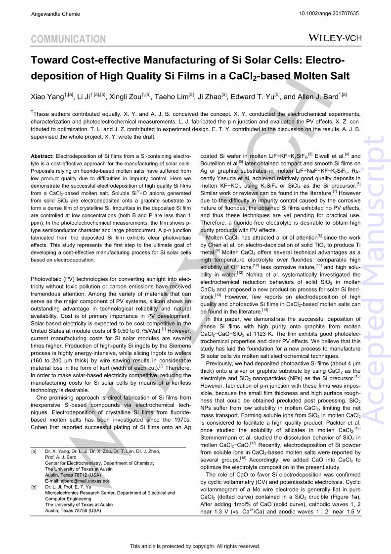
The role of CaO to favor Si electrodeposition was confirmed
by cyclic voltammetry (CV) and potentiostatic electrolysis. Cyclic
voltammogram of a Mo wire electrode is generally flat in pure
CaCl2 (dotted curve) contained in a SiO2 crucible (Figure 1a).
After adding 1mol% of CaO (solid curve), cathodic waves 1, 2
near 1.3 V (vs. Ca2+
/Ca) and anodic waves 1`, 2` near 1.5 V
[a] Dr. X. Yang, Dr. L. Ji, Dr. X. Zou, Dr. T. Lim, Dr. J. Zhao,
Prof. A. J. Bard
Center for Electrochemistry, Department of Chemistry
The University of Texas at Austin
Austin, Texas 78712 (USA)
E-mail: [email protected]
[b] Dr. L. Ji, Prof. E. T. Yu
Microelectronics Research Center, Department of Electrical and
Computer Engineering
The University of Texas at Austin
Austin, Texas 78758 (USA)
10.1002/ange.201707635Angewandte Chemie
This article is protected by copyright. All rights reserved.
COMMUNICATION
appear clearly. CVs conducted in a larger potential range (Fig-
ure S3) indicate the same tendency. EDS analysis of the product
on a graphite plate cathode after potentiostatic electrolysis at 0.7
V (vs. Ca2+
/Ca) for 10 min in molten CaCl2−CaO(1mol%) con-
firms formation of Si on the cathode surface (Figure 1b). It is
proposed that O2-
ions dissociated from CaO react with the SiO2
crucible to generate soluble SiIV
−O complex anions. Therefore,
we can attribute waves 1 and 2 to deposition of Si from SiIV
−O
anions, and waves 1`, 2` to re-oxidation of Si. However, for-
mation mechanism and electrochemical behavior of SiIV
−O
anions in molten CaCl2 are not well understood.
Figure 1. a) Cyclic voltammograms of a Mo wire in molten CaCl2 and
CaCl2−CaO(1mol%) in a SiO2 crucible at 1123 K and b) a photograph of a
graphite plate cathode after potentiostatic electrolysis at 0.7 V (vs. Ca2+
/Ca) for
10 min in molten CaCl2−CaO(1mol%) in a SiO2 crucible at 1123 K and the
EDS spectrum of the product on the surface.
We tried to electrodeposit Si films onto graphite in molten
CaCl2 with addition of different amounts of CaO. SiO2 NPs were
used as the Si precursor to favor a fast dissolution. According to
the product quality, we find that CaCl2 with addition of 4.8mol%
of CaO and 3.9mol% of SiO2 NPs is the optimum composition.
Excess CaO induces formation of Ca metal while excess SiO2
NPs causes difficulty in complete dissolution in a short time.
SiO2 NPs suspended in the melt tend to form Si powders on
cathode via direct electrochemical reduction (Figure S4). [13a]
By optimizing the electrolyte composition, we made significant
progress in film thickness and quality compared with our previ-
ous work.[15]
Dense crystalline Si films (thickness up to 35 μm)
were deposited onto a graphite substrate by constant current
electrolysis in the two-electrode manner (Figures 2 and S5). The
current of 15 mA cm-2
is considered an optimum value (Figure
S6). Formation mechanism is proposed in Figure 3. In the mol-
ten salt, solid SiO2 NPs react with O2-
to form soluble SiIV
−O
anions, which are reduced to Si atoms on the graphite surface
by obtaining electrons. A uniform Si film is gradually formed after
nucleation and crystallization. O2-
isolated from SiIV
−O anions
diffuse toward the graphite anode and leave the system as CO
or CO2. Increase of film thickness and grain size indicates the
continuous progress of electrodeposition and crystallization.
Current efficiency is about 40% to form the 20 μm film (Figure
S7). However, the film formation efficiency decreases with elec-
trolysis time. Accumulation of powders on film surface during
electrolysis is the reason for the decreasing efficiency. We be-
lieve that generating soluble SiIV
−O anions to a certain concen-
tration while getting rid of suspended SiO2 particles in molten
salt are the keys to produce a good film.
Figure 2. SEM images of the Si films deposited on graphite substrates in
molten CaCl2−CaO−SiO2(CaO:4.8mol%, SiO2:3.9mol%) at 1123 K by electrol-
ysis at a constant cathodic current of 15 mA cm-2
for a) 1 h, b) 3 h and c) 7 h.
Figure 3. A schematic illustration of the formation mechanism of Si film onto a
graphite substrate by electrodeposition in molten CaCl2−CaO−SiO2.
Chemical composition of a deposited Si film was analyzed by
glowing discharge mass spectrometry (GDMS). The result (Ta-
ble 1) indicates low impurity concentrations. B and P, both re-
garded as the most problematic elements for solar Si, are 0.9
ppm and 0.6 ppm, respectively. Other impurities except Ca and
Cl are all less than 10 ppm. We consider that residual CaCl2 on
the film surface due to insufficient rinsing is the major source of
Ca and Cl. However, thermodynamic data (Figure S8) implies
that decomposition of CaO is possible during electrolysis to form
dilute Ca-Si alloys because of the small activity of Ca in Si.[19]
We will investigate the alloys formation by checking the chemical
state of Ca in the future study. Na, Mg and Al may come from
CaCl2. W is from the electrode material. Other impurities may
also derive from CaCl2 or the SiO2 crucible. We believe that
there is large room for further improvement by using high-purity
raw materials and optimizing the operation. Our progress indi-
cates good prospects of high-purity Si production via electro-
chemical techniques using CaCl2-based molten salts.
10.1002/ange.201707635Angewandte Chemie
This article is protected by copyright. All rights reserved.
COMMUNICATION
Table 1. Chemical composition of a Si film deposited at a constant cathodic
current of 15 mA cm-2
for 3 h in molten CaCl2−CaO−SiO2(CaO:4.8mol%,
SiO2:3.9mol%) at 1123 K, analyzed by GDMS.
Element[a]
Concentration[b]
Element Concentration
B 0.9 Ca 250
F <5 Ti 0.9
Na 6.9 Mn 0.7
Mg 5.7 Fe <0.5
Al 10 Cu 4.8
P 0.6 Br 3.2
S 2 Zr 2.2
Cl 330 W 13
[a] C, H, and O are not determined; impurities less than 0.5 ppm are not listed.
[b] Unit: ppm by weight.
In photoelectrochemical measurements, the deposited Si films
exhibit a p-type semiconductor character: shift of open circuit
potentials to more positive values under illumination due to
movement of the positively charged holes away from the surface
toward the Si bulk (Figure 4a). Because of flowing of excited
electrons in the conduction band across the semiconduc-
tor/solution interface, ethyl viologen cations (EV2+
) in the solution
are reduced into EV+, and cathodic photocurrent is induced
(Figure 4b). According to the impurity concentrations (Table 1),
we consider that Al having three valence electrons is most likely
the dominant p-type dopant for the deposited Si films. Doping
proceeds electrochemically during electrodeposition. However,
the doping mechanism is not well understood.
Figure 4. a) Variation of open circuit potentials for the deposited Si films and
b) photocurrent-potential characteristics for the deposited Si films and a p-type
Si wafer in darkness and under illumination at 100 mW cm-2
. Light was
chopped at an interval of 2 s.
Shift of open circuit potential by illumination from darkness for
the 20 μm film (about 0.25 V) is larger compared with that of the
7 μm film (about 0.11 V), indicating the difference in the amount
of excited electrons. Larger film thickness and higher film quality
result in better photoelectrochemical properties. In the case of
the thinner film (7 μm), photocurrent is 1.1 mA cm-2
at -0.62 V
(vs. Ag/AgNO3). Dark current originating from the exposed
graphite surface increases at more negative potentials, indicat-
ing many undesired pinholes or cracks in the film. For the thicker
film (20 μm), photocurrent reaches 3.3 mA cm-2
at -0.62 V (vs.
Ag/AgNO3), amounting to 36% that of the commercial p-type Si
wafer (about 9.1 mA cm-2
), while dark current is relatively small
even at more negative potentials. According to replicated meas-
urements on the same sample, we found good stability of the
photoelectrochemical properties of the deposited film. Large
photocurrent implies the high purity of the deposited Si films,
although still not as large as the commercial wafer.
Due to the improved film quality, a p-n junction was success-
fully fabricated by using the 20 μm Si film (Figure S2). As indi-
cated by current-voltage characteristics (Figure 5), the junction
exhibits good diode rectifying behaviour in darkness (dotted
curve) and clear PV effects under illumination (solid curve).
When illuminated, open circuit potential (Voc) is 52 mV, short
circuit current (Jsc) is 3.3 mA cm-2
, and power conversion effi-
ciency (PCE) is estimated to be about 0.1%.
Figure 5. Current-voltage characteristics of a p-n junction fabricated from the
deposited Si film in darkness and under illumination (AM1.5G, 100 mW cm-2
).
To the best of our knowledge, this is the first report on elec-
trodeposition of Si films exhibiting clear PV effects. Optimization
of parameters and implementation of post-treatments are likely
to improve the film quality to approach or satisfy the require-
ments of a commercial application. Accordingly, we propose a
new process via molten salt electrodeposition to manufacture Si
solar cells. Multiple steps (primary reduction and downstream
casting & slicing, doping) in the conventional process are inte-
grated into one step (electrodeposition) in the new process
(Figure 6). Dopant type and concentration could be controlled by
adjusting additive type and quantity in molten salt. Therefore, a
considerable cost reduction with the new process would be
expected. The process could be further simplified by formation
of the p-n junction electrochemically, which is currently being
investigated.
10.1002/ange.201707635Angewandte Chemie
This article is protected by copyright. All rights reserved.
COMMUNICATION
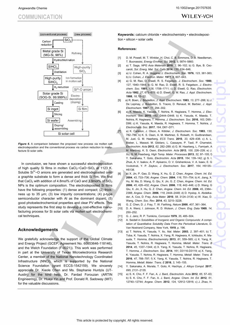
Figure 6. A comparison between the proposed new process via molten salt
electrodeposition and the conventional process via carbon reduction to manu-
facture Si solar cells.
In conclusion, we have shown a successful electrodeposition
of high quality Si films in molten CaCl2−CaO−SiO2 at 1123 K.
Soluble SiIV
−O anions are generated and electrodeposited onto
a graphite substrate to form a dense and thick Si film. We find
that CaCl2 with addition of 4.8mol% of CaO and 3.9mol% of SiO2
NPs is the optimum composition. The electrodeposited Si films
have the following properties: (1) dense and compact; (2) thick-
ness up to 35 μm; (3) low impurity concentrations; (4) p-type
semiconductor character with Al as the dominant dopant; (5)
good photoelectrochemical properties and clear PV effects. This
study represents the first step to develop a cost-effective manu-
facturing process for Si solar cells via molten salt electrochemi-
cal techniques.
Acknowledgements
We gratefully acknowledge the support of the Global Climate
and Energy Project (GCEP, Agreement No. 60853646-118146),
and the Welch Foundation (F-0021)). This work was performed
in part at the University of Texas Microelectronics Research
Center, a member of the National Nanotechnology Coordinated
Infrastructure (NNCI), which is supported by the National
Science Foundation (grant ECCS-1542159). We sincerely
appreciate Dr. Xiaole Chen and Ms. Stephanie Huntzis (UT-
Austin) for the kind help, Dr. Fardad Forouzan (ARTIN
Engineering), Dr. Huayi Yin and Prof. Donald R. Sadoway (MIT)
for the valuable discussions.
Keywords: calcium chloride • electrochemistry • electrodeposi-
tion • silicon • solar cells
References:
[1] D. M. Powell, M. T. Winkler, H. Choi, C. B. Simmons, D. B. Needleman,
T. Buonassisi, Energy Environ. Sci. 2012, 5, 5874–5883.
[2] a) T. Saga, NPG Asia Materials 2010, 2, 96–102; b) G. Bye, B. Cec-
caroli, Sol. Energ. Mat. Sol. Cells 2014, 130, 634–646.
[3] a) U. Cohen, R. A. Huggins, J. Electrochem. Soc. 1976, 123, 381-383;
b) U. Cohen, J. Electron. Mater. 1977, 6, 607–643.
[4] a) G. M. Rao, D. Elwell, R. S. Feigelson, J. Electrochem. Soc. 1980,
127, 1940–1944; b) G. M. Rao, D. Elwell, R. S. Feigelson, J. Electro-
chem. Soc. 1981, 128, 1708–1711; c) D. Elwell, G. Rao, Electrochim.
Acta 1982, 27, 673–676; d) D. Elwell, G. M. Rao, J. Appl. Electrochem.
1988, 18, 15–22.
[5] a) R. Boen, J. Bouteillon, J. Appl. Electrochem. 1983, 13, 277–288; b) J.
De Lepinay, J. Bouteillon, S. Traore, D. Renaud, M. Barbier, J. Appl.
Electrochem. 1987, 17, 294–302.
[6] a) K. Maeda, K. Yasuda, T. Nohira, R. Hagiwara, T. Homma, J. Elec-
trochem. Soc. 2015, 162, D444–D448; b) K. Yasuda, K. Maeda, T.
Nohira, R. Hagiwara, T. Homma, J. Electrochem. Soc. 2016, 163, D95–
D99; c) K. Yasuda, K. Maeda, R. Hagiwara, T. Homma, T. Nohira, J.
Electrochem. Soc. 2017, 164, D67–D71.
[7] a) K. Carleton, J. Olson, A. Kibbler, J. Electrochem. Soc. 1983, 130,
782–786; b) K. S. Osen, A. M. Martinez, S. Rolseth, H. Gudbrandsen,
M. Juel, G. M. Haarberg, ECS Trans. 2010, 33, 429–438; c) A. L.
Bieber, L. Massot, M. Gibilaro, L. Cassayre, P. Taxil, P. Chamelot,
Electrochim. Acta 2012, 62, 282–289; d) G. M. Haarberg, L. Famiyeh, A.
M. Martinez, K. S. Osen, Electrochim. Acta 2013, 100, 226–228; e) J.
Xu, G. M. Haarberg, High Temp. Mater. Processes 2013, 32, 97–105; f)
Y. Sakanaka, T. Goto, Electrochim. Acta 2015, 164, 139–142; g) S. I.
Zhuk, A. V. Isakov, A. P. Apisarov, O. V. Grishenkova, V. A. Isaev, E. G.
Vovkotrub, Y. P. Zaykov, J. Electrochem. Soc. 2017, 164, H5135–
H5138.
[8] a) X. Jin, P. Gao, D. Wang, X. Hu, G. Z. Chen, Angew. Chem. Int. Ed.
2004, 43, 733–736; Angew. Chem. 2004, 116, 751–754; b) K. Jiang, X.
Hu, M. Ma, D. Wang, G. Qiu, X. Jin, G. Z. Chen, Angew. Chem. Int. Ed.
2006, 45, 428–432; Angew. Chem. 2006, 118, 442–446; c) D. Wang, G.
Qiu, X. Jin, X. Hu, G. Z. Chen, Angew. Chem. Int. Ed. 2006, 45, 2384–
2388; Angew. Chem. 2006, 118, 2444–2448; d) D. Hyslop, A. Abdelka-
der, A. Cox, D. Fray, Acta Mater. 2010, 58, 3124–3130; e) W. Xiao, D.
Wang, Chem. Soc. Rev. 2014, 43, 3215–3228.
[9] G. Z. Chen, D. J. Fray, T. W. Farthing, Nature 2000, 407, 361–364.
[10] D. A. Wenz, I. Johnson, R. D. Wolson, J. Chem. Eng. Data 1969, 14,
250–252.
[11] G. J. Janz, R. P. Tomkins, Corrosion 1979, 35, 485–504.
[12] A. Seidell in Solubilities of Inorganic and Organic Compounds: A compi-
lation of Quantitative Solubility Data From the Periodical Literature, D.
Van Nostrand Company, New York, 1919, p. 196.
[13] a) T. Nohira, K. Yasuda, Y. Ito, Nat. Mater. 2003, 2, 397–401; b) T.
Toba, K. Yasuda, T. Nohira, X. Yang, R. Hagiwara, K. Ichitsubo, K. Ma-
suda, T. Homma, Electrochemistry 2013, 81, 559–565; c) X. Yang, K.
Yasuda, T. Nohira, R. Hagiwara, T. Homma, Metall. Mater. Trans. B
2014, 45, 1337–1344; d) X. Yang, K. Yasuda, T. Nohira, R. Hagiwara,
T. Homma, J. Electrochem. Soc. 2014, 161, D3116-D3119; e) X. Yang,
K. Yasuda, T. Nohira, R. Hagiwara, T. Homma, Metall. Mater. Trans. B
2016, 47, 788–797; f) X. Yang, K. Yasuda, T. Nohira, R. Hagiwara, T.
Homma, Metall. Mater. Trans. E 2016, 3, 145–155.
[14] Y. Sakanaka, A. Murata, T. Goto, K. Hachiya, J. Alloys Compd. 2017,
695, 2131–2135.
[15] a) S. K. Cho, F. F. Fan, A. J. Bard, Electrochim. Acta 2012, 65, 57–63;
b) S. K. Cho, F. F. Fan, A. J. Bard, Angew. Chem. Int. Ed. 2012, 51,
12740–12744; Angew. Chem. 2012, 124, 12912-12916; c) J. Zhao, H.
10.1002/ange.201707635Angewandte Chemie
This article is protected by copyright. All rights reserved.

COMMUNICATION
Yin, T. Lim, H. Xie, H. Hsu, F. Forouzan, A. J. Bard, J. Electrochem.
Soc. 2016, 163, D506–D514.
[16] A. Packter, S. Zaidi, Z. Phys. Chem. 1982, 263, 481–489.
[17] P. Stemmermann, H. Pöllmann, N. Jb. Miner. Mh. 1992, 9, 409–431.
[18] a) O. E. Kongstein, C. Wollan, S. Sultana, G. M. Haarberg, ECS Trans.
2007, 35, 357–361; b) J. Cai, X. Luo, G. M. Haarberg, O. E. Kongstein,
S. Wang, J. Electrochem. Soc. 2012, 159: D155–D158; c) K. Yasuda, T.
Nohira, R. Hagiwara, Y. H. Ogata, J. Electrochem. Soc. 2007, 154,
E95–E101; d) W. Xiao, X. Wang, H. Yin, H. Zhu, X. Mao, D. Wang,
RSC Adv. 2012, 2, 7588–7593.
[19] J. R. Wynnyckyj, L. M. Pidgeon, Metall. Trans. 1971, 2, 975–978.
10.1002/ange.201707635Angewandte Chemie
This article is protected by copyright. All rights reserved.
COMMUNICATION
Entry for the Table of Contents
Layout 1:
COMMUNICATION
A novel approach to fabricate high
quality Si films for photovoltaic appli-
cations is developed by electrodeposi-
tion from molten CaCl2−CaO−SiO2.
Soluble SiIV
−O anions generated from
solid SiO2 are electrodeposited onto a
graphite substrate to form a dense
and thick film of p-type Si. Impurities
in the deposited Si film are controlled
at low concentrations. The film exhib-
its good photoelectrochemical proper-
ties and clear photovoltaic effects.
Xiao Yang, Li Ji, Xingli Zou, Taeho Lim,
Ji Zhao, Edward T. Yu, and
Allen J. Bard*,
Page No. – Page No.
Toward Cost-effective Manufacturing
of Si Solar Cells: Electrodeposition of
High Quality Si Films in a CaCl2-
based Molten Salt
10.1002/ange.201707635Angewandte Chemie
This article is protected by copyright. All rights reserved.