Embed Size (px)
Citation preview
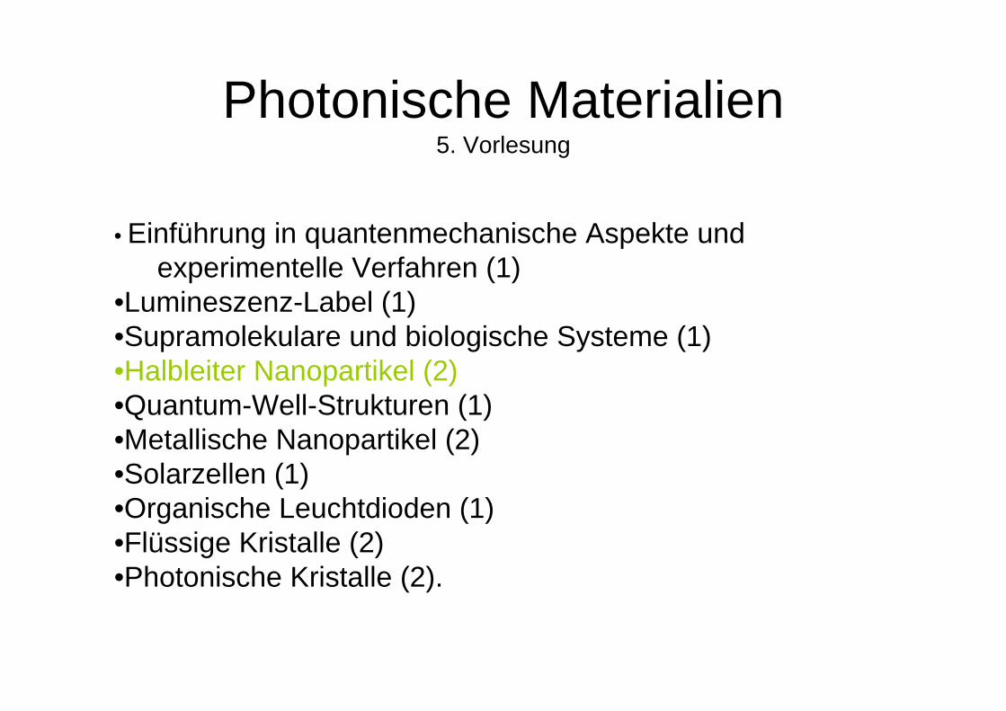
Photonische Materialien5. Vorlesung
• Einführung in quantenmechanische Aspekte und experimentelle Verfahren (1)
•Lumineszenz-Label (1)•Supramolekulare und biologische Systeme (1)•Halbleiter Nanopartikel (2)•Quantum-Well-Strukturen (1) •Metallische Nanopartikel (2)•Solarzellen (1)•Organische Leuchtdioden (1)•Flüssige Kristalle (2)•Photonische Kristalle (2).
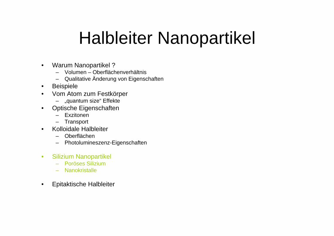
Halbleiter Nanopartikel• Warum Nanopartikel ?
– Volumen – Oberflächenverhältnis– Qualitative Änderung von Eigenschaften
• Beispiele• Vom Atom zum Festkörper
– „quantum size“ Effekte• Optische Eigenschaften
– Exzitonen– Transport
• Kolloidale Halbleiter– Oberflächen– Photolumineszenz-Eigenschaften
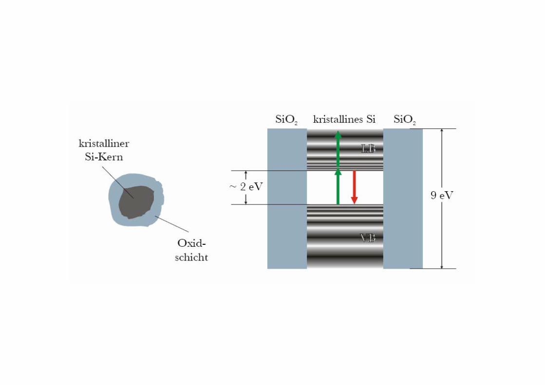
• Silizium Nanopartikel– Poröses Silizium– Nanokristalle
• Epitaktische Halbleiter
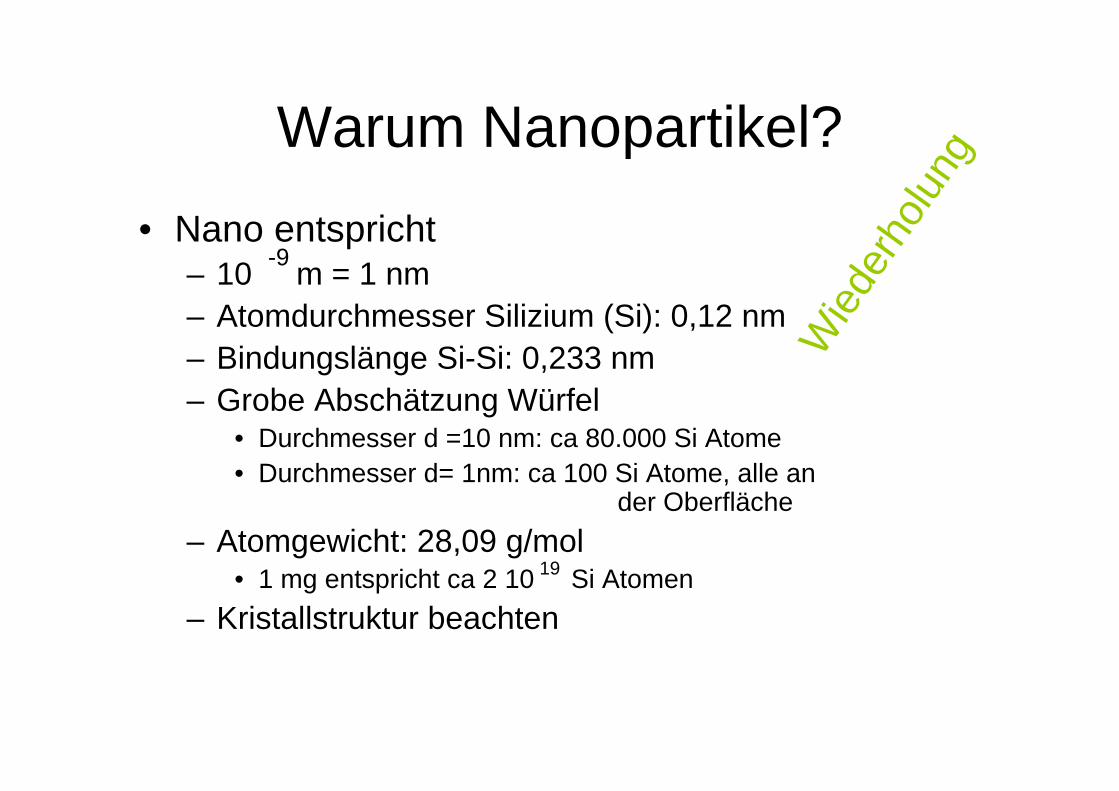
Warum Nanopartikel?• Nano entspricht
– 10 m = 1 nm– Atomdurchmesser Silizium (Si): 0,12 nm– Bindungslänge Si-Si: 0,233 nm– Grobe Abschätzung Würfel
• Durchmesser d =10 nm: ca 80.000 Si Atome• Durchmesser d= 1nm: ca 100 Si Atome, alle an
der Oberfläche– Atomgewicht: 28,09 g/mol
• 1 mg entspricht ca 2 10 Si Atomen– Kristallstruktur beachten
-9
19
Wied
erho
lung
Warum Nanopartikel?
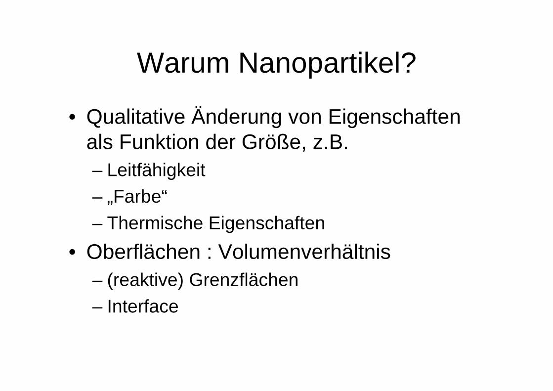
• Qualitative Änderung von Eigenschaften als Funktion der Größe, z.B. – Leitfähigkeit– „Farbe“– Thermische Eigenschaften
• Oberflächen : Volumenverhältnis– (reaktive) Grenzflächen– Interface
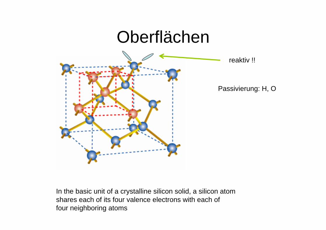
Oberflächen
In the basic unit of a crystalline silicon solid, a silicon atomshares each of its four valence electrons with each of four neighboring atoms
Passivierung: H, O
reaktiv !!
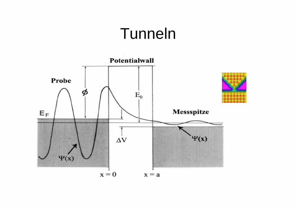
Tunneln
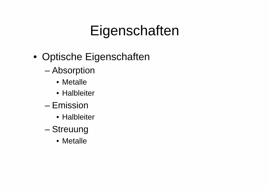
Eigenschaften
• Optische Eigenschaften– Absorption
• Metalle• Halbleiter
– Emission• Halbleiter
– Streuung• Metalle
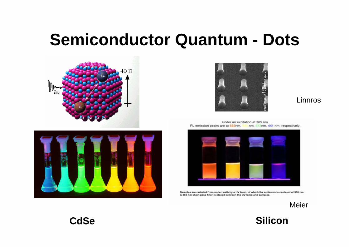
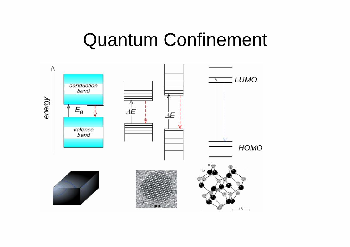
Semiconductor Quantum - Dots
CdSe Silicon
Linnros
Meier
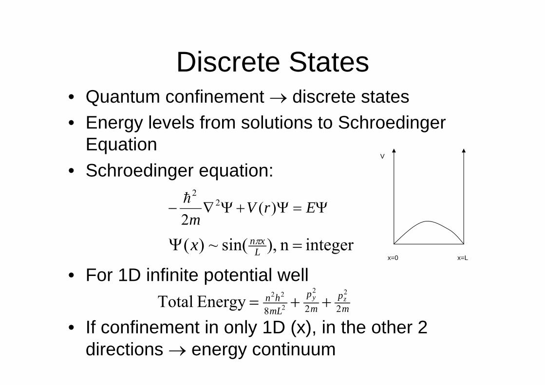
Discrete States• Quantum confinement → discrete states• Energy levels from solutions to Schroedinger
Equation• Schroedinger equation:
• For 1D infinite potential well
• If confinement in only 1D (x), in the other 2 directions → energy continuum
Ψ=Ψ+Ψ∇− ErVm
)(2
22h
integer n ,)sin(~)( =Ψ Lxnx π
mp
mp
mLhn zy
228
22
2
22Energy Total ++=
x=0 x=L
V
Quantum Confinement
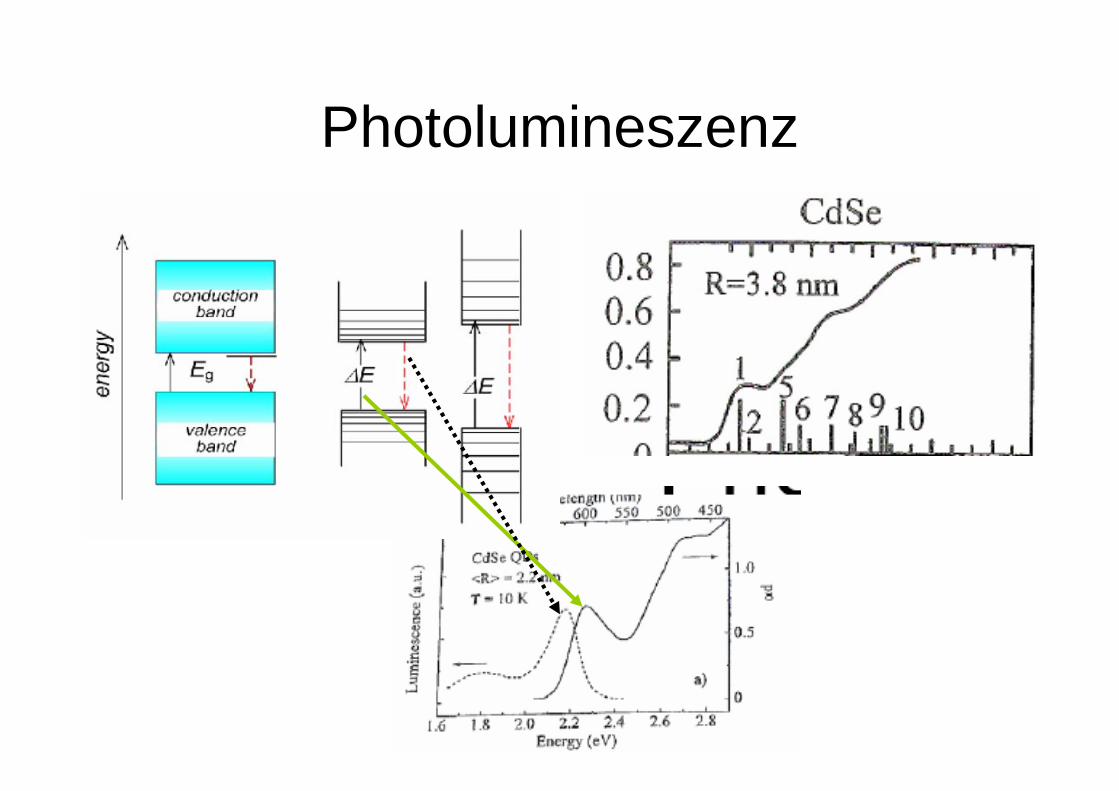
Photolumineszenz
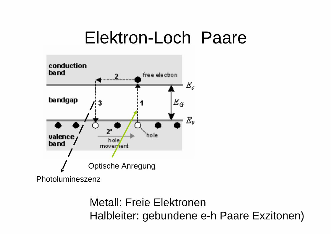
Elektron-Loch Paare
Optische Anregung
Metall: Freie ElektronenHalbleiter: gebundene e-h Paare Exzitonen)
Photolumineszenz
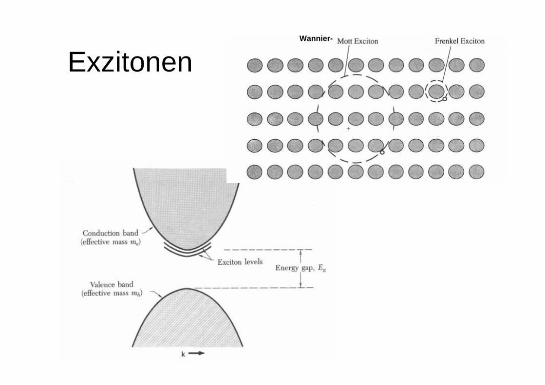
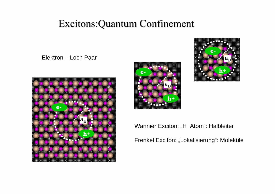
ExzitonenWannier-
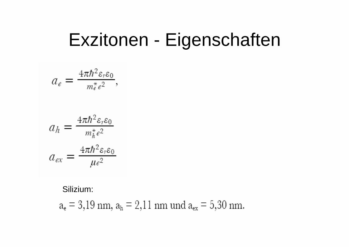
Exzitonen - Eigenschaften
Silizium:
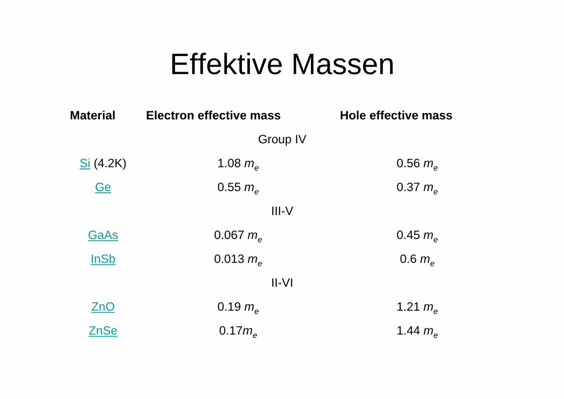
Effektive Massen
1.44 me0.17meZnSe
1.21 me0.19 meZnO
II-VI
0.6 me0.013 meInSb
0.45 me0.067 meGaAs
III-V
0.37 me0.55 meGe
0.56 me1.08 meSi (4.2K)
Group IV
Hole effective massElectron effective massMaterial
h+
e-
aB
h+
e-
aB
h+
e-aB
Excitons:QuantumExcitons:Quantum ConfinementConfinement
Elektron – Loch Paar
Wannier Exciton: „H_Atom“: Halbleiter
Frenkel Exciton: „Lokalisierung“: Moleküle
Eg Eg Eg
)h(rhV)e(reVhrer2ε
2e2h
h2m
22e
e2m
2H ++
−−∇−∇−=
hh
*
2
2
2
22
10 248.0786.1112 Ryd
he
ERe
mmRE −−⎥
⎦
⎤⎢⎣
⎡+=
επh
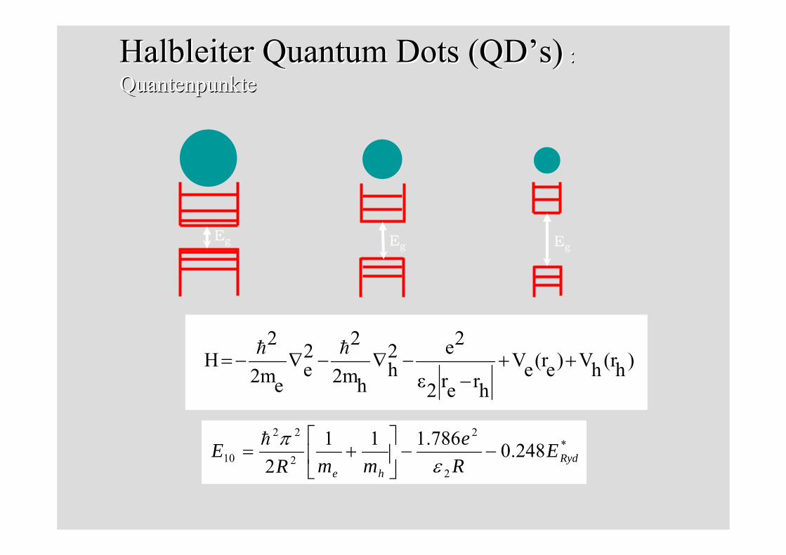
HalbleiterHalbleiter Quantum Dots (QDQuantum Dots (QD’’s)s) ::QuantenpunkteQuantenpunkte
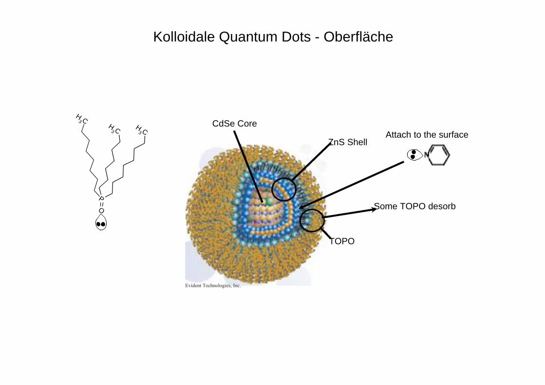
TOPO
ZnS Shell
CdSe Core
Kolloidale Quantum Dots - Oberfläche
Evident Technologies, Inc.
Attach to the surface
Some TOPO desorbP
CH3 CH
3
CH3
O
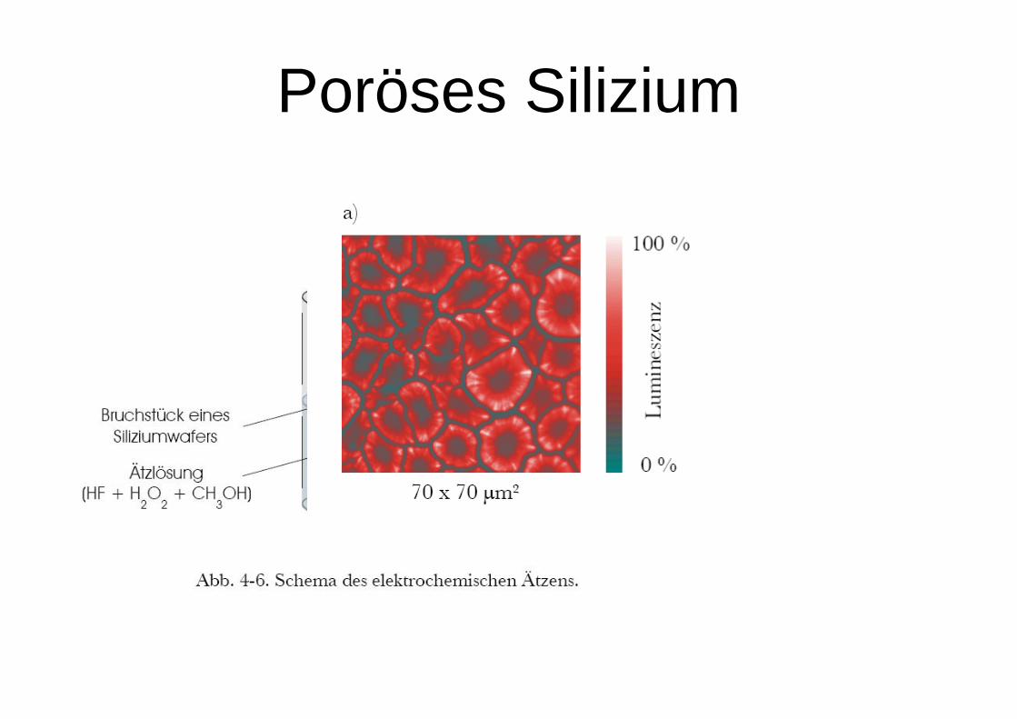
Poröses Silizium
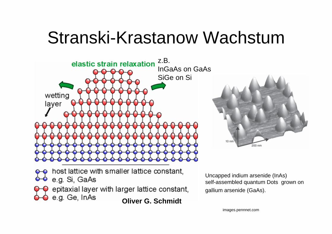
Stranski-Krastanow Wachstum z.B. InGaAs on GaAs SiGe on Si
Oliver G. Schmidt
Uncapped indium arsenide (InAs) self-assembled quantum Dots grown on gallium arsenide (GaAs).
images.pennnet.com
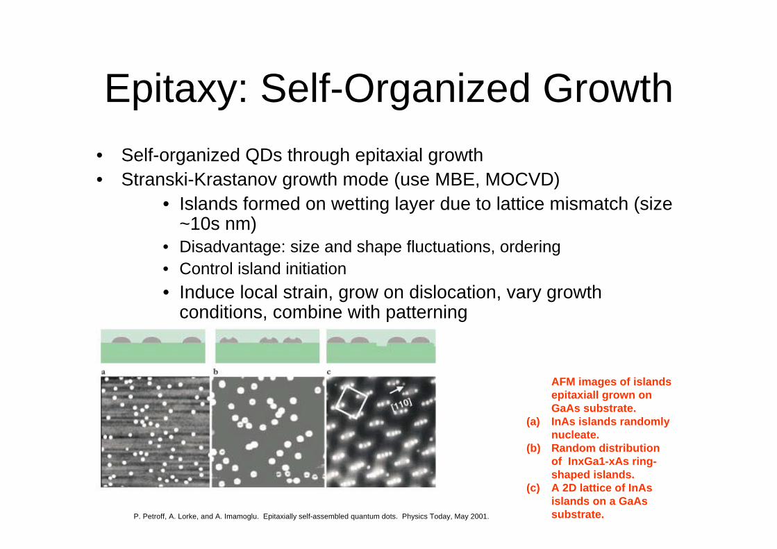
Epitaxy: Self-Organized Growth• Self-organized QDs through epitaxial growth • Stranski-Krastanov growth mode (use MBE, MOCVD)
• Islands formed on wetting layer due to lattice mismatch (size ~10s nm)
• Disadvantage: size and shape fluctuations, ordering• Control island initiation • Induce local strain, grow on dislocation, vary growth
conditions, combine with patterning
AFM images of islands epitaxiall grown on GaAs substrate.
(a) InAs islands randomly nucleate.
(b) Random distribution of InxGa1-xAs ring-shaped islands.
(c) A 2D lattice of InAsislands on a GaAssubstrate. P. Petroff, A. Lorke, and A. Imamoglu. Epitaxially self-assembled quantum dots. Physics Today, May 2001.
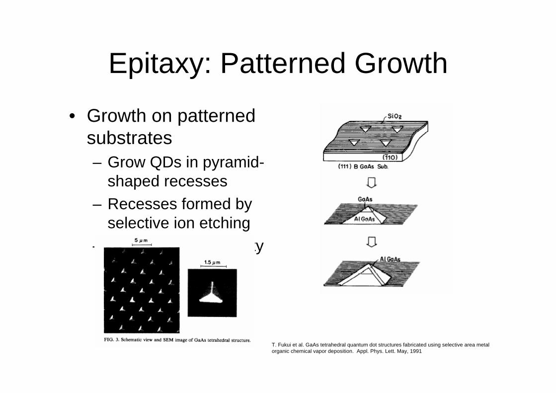
Epitaxy: Patterned Growth
• Growth on patterned substrates – Grow QDs in pyramid-
shaped recesses– Recesses formed by
selective ion etching– Disadvantage: density
of QDs limited by mask pattern
T. Fukui et al. GaAs tetrahedral quantum dot structures fabricated using selective area metal organic chemical vapor deposition. Appl. Phys. Lett. May, 1991
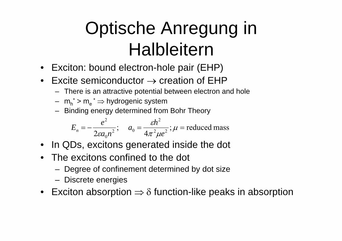
Optische Anregung in Halbleitern
• Exciton: bound electron-hole pair (EHP)• Excite semiconductor → creation of EHP
– There is an attractive potential between electron and hole– mh
* > me * ⇒ hydrogenic system
– Binding energy determined from Bohr Theory
• In QDs, excitons generated inside the dot• The excitons confined to the dot
– Degree of confinement determined by dot size– Discrete energies
• Exciton absorption ⇒ δ function-like peaks in absorption
mass reduced ;4
;2 22
2
020
2
==−= μμπ
εε e
hana
eEn
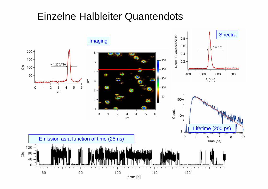
Emission as a function of time (25 ns)
Einzelne Halbleiter Quantendots
Imaging
Lifetime (200 ps)
Spectra
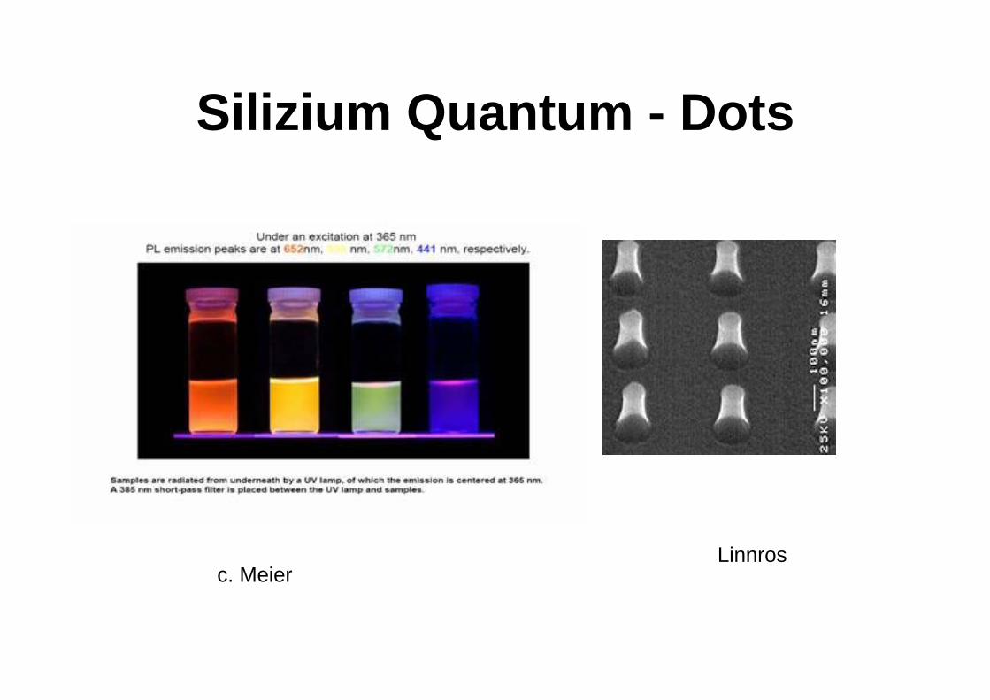
Silizium Quantum - Dots
Linnrosc. Meier
Si Quantendots
Christian von Borczyskowski
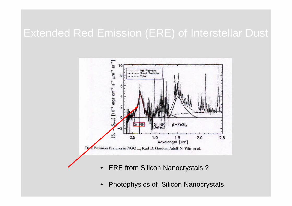
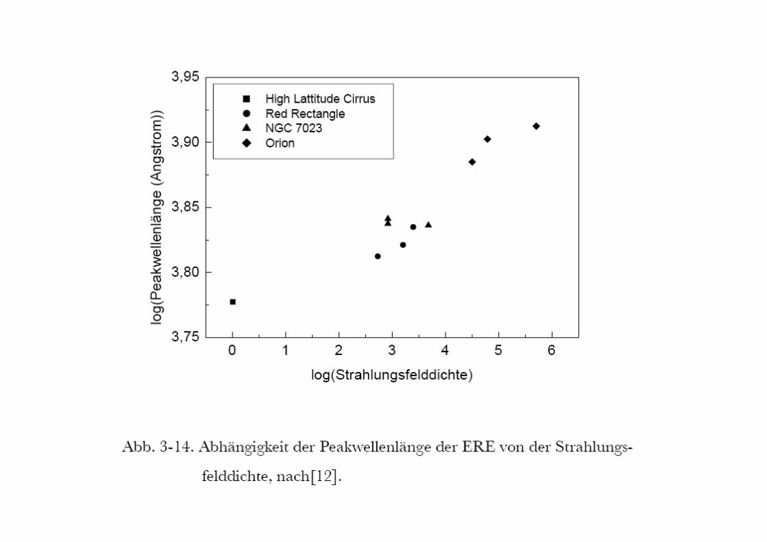
Extended Red Emission (ERE) of Interstellar Dust
• ERE from Silicon Nanocrystals ?
• Photophysics of Silicon Nanocrystals
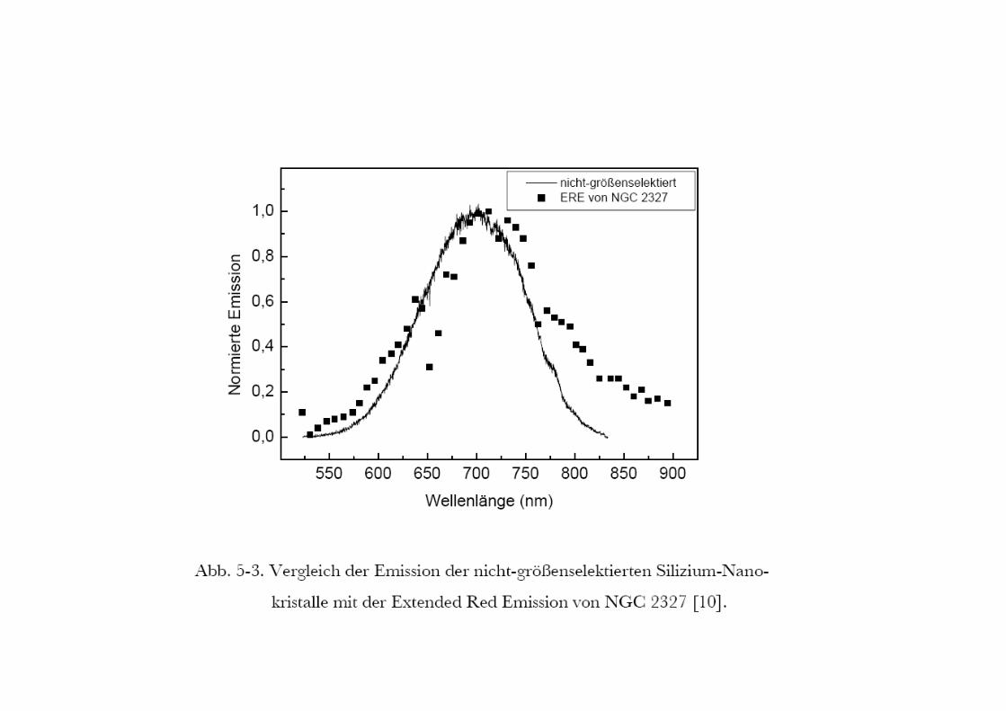
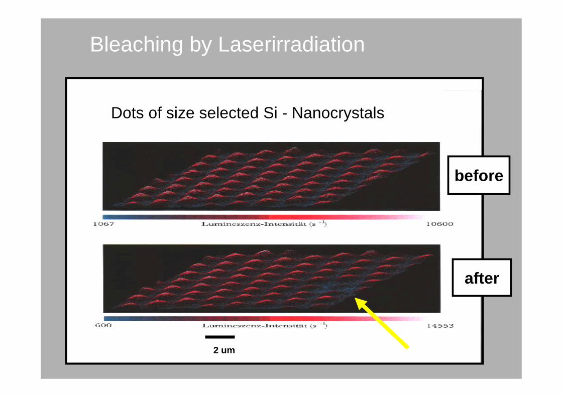
Dots of size selected Si - Nanocrystals
Bleaching by Laserirradiation
2 um
after
before
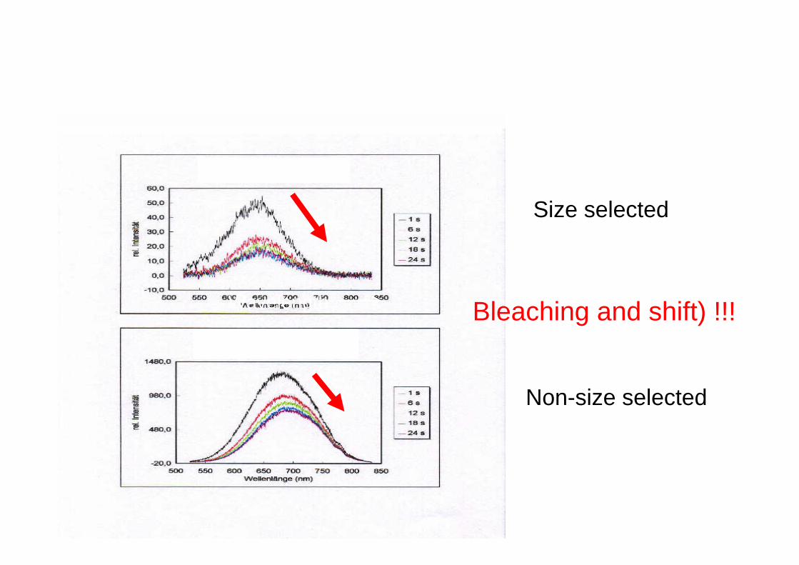
Si-NC Bleaching and Spectral Shifts
Size selected
Non-size selected
Wavelength Bleaching and shift) !!!
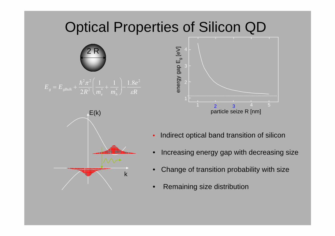
Optical Properties of Silicon QD2 R
• Indirect optical band transition of silicon
• Increasing energy gap with decreasing size
• Change of transition probability with size
• Remaining size distribution
2 3 4 51
4
3
2
1
particle seize R [nm]
ener
gy g
ap E
g[e
V]
Eg = EgBulk +
h2π 2
2R21
me* +
1mh
*
⎛
⎝ ⎜
⎞
⎠ ⎟ −
1.8e2
εR
E(k)
k
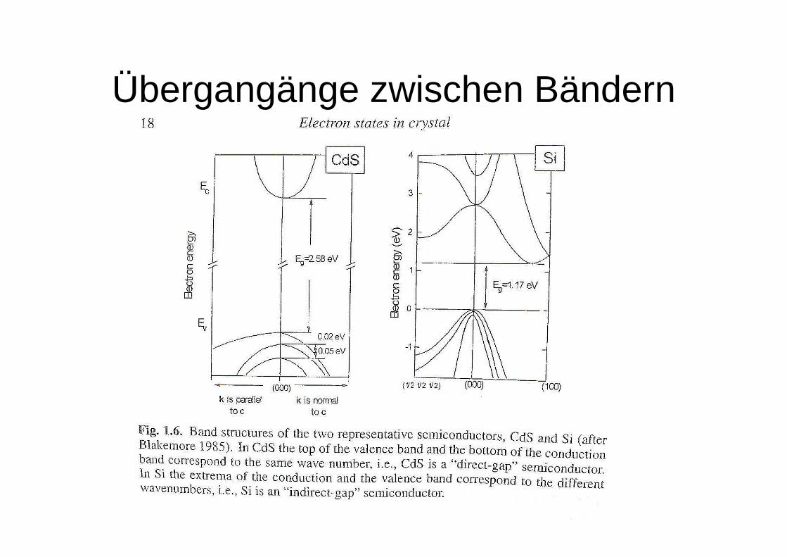
Übergangänge zwischen Bändern
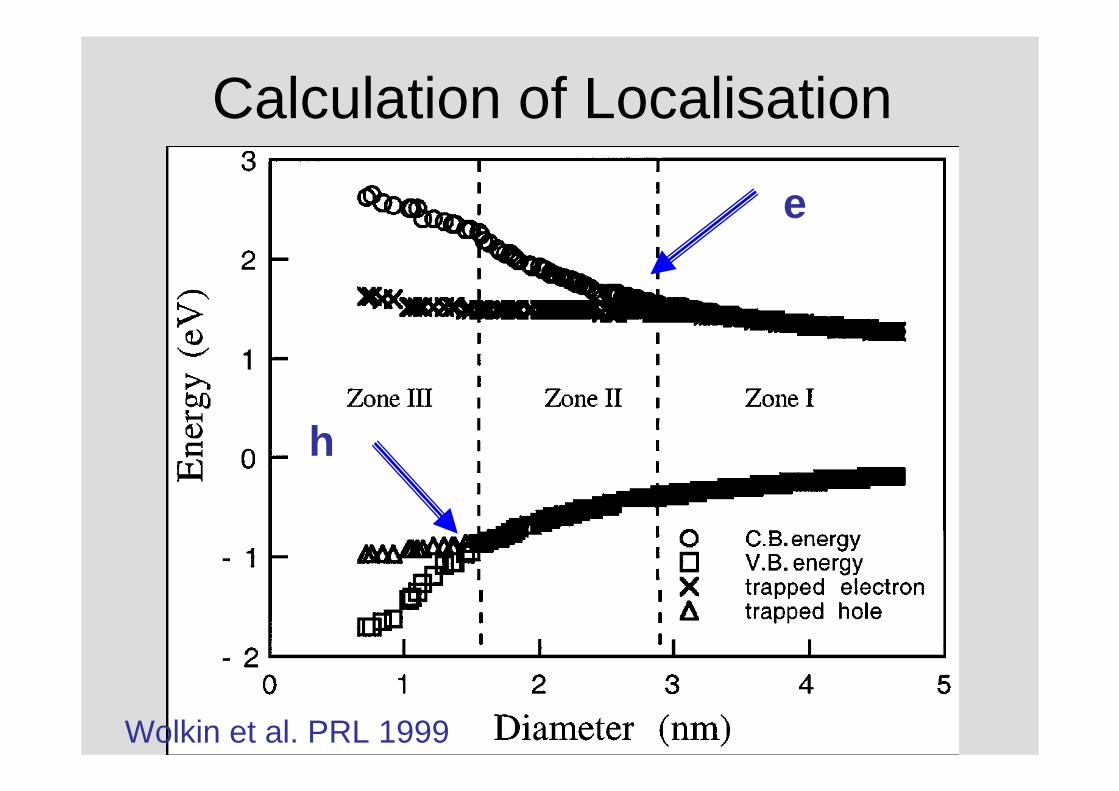
Calculation of Localisation
e
h
Wolkin et al. PRL 1999
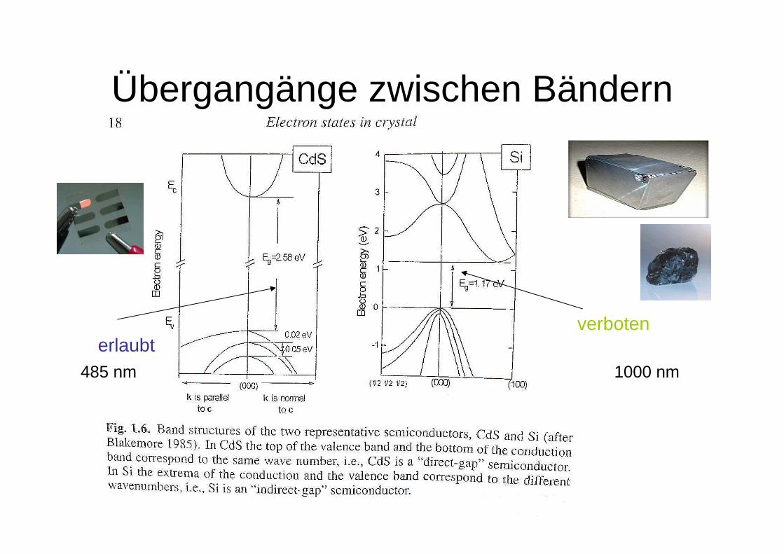
Übergangänge zwischen Bändern
erlaubtverboten
1000 nm485 nm
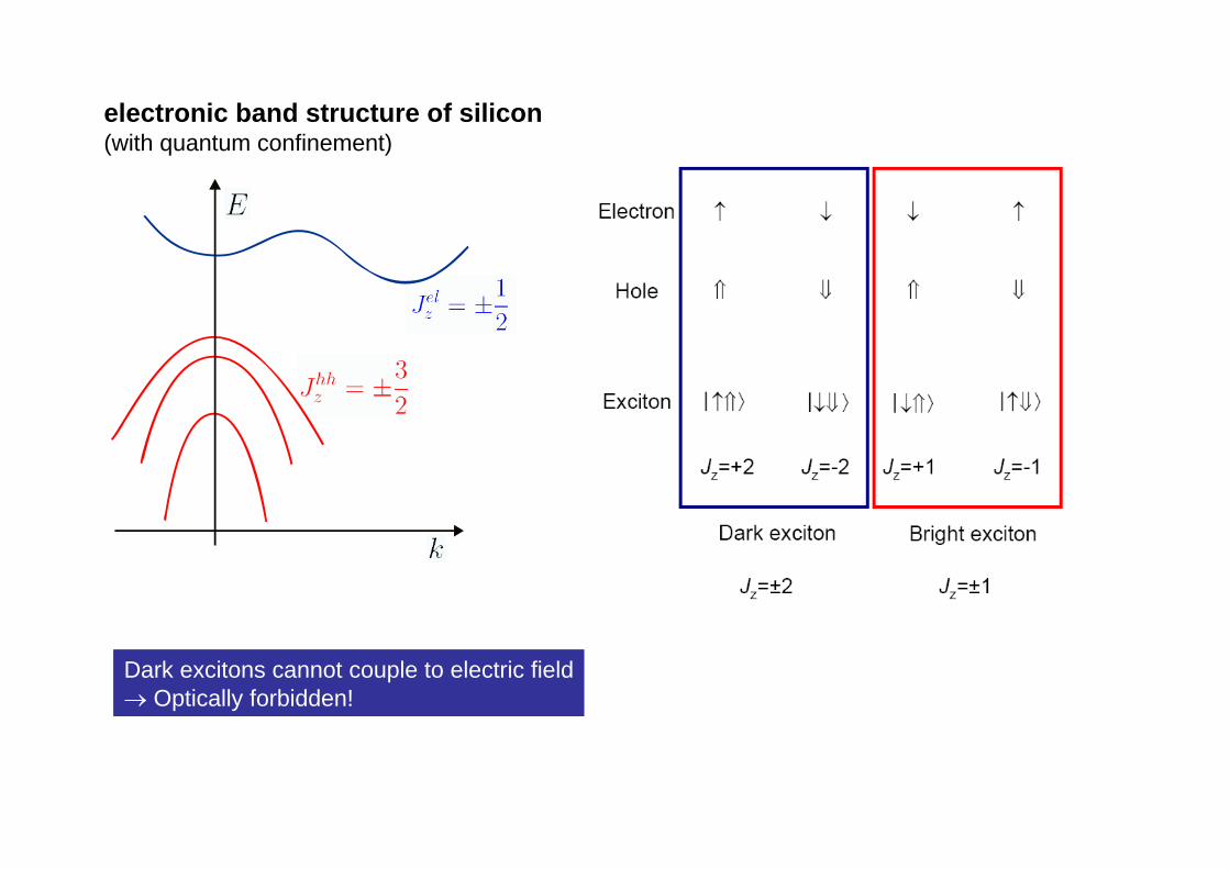
electronic band structure of silicon(with quantum confinement)
Dark excitons cannot couple to electric field→ Optically forbidden!
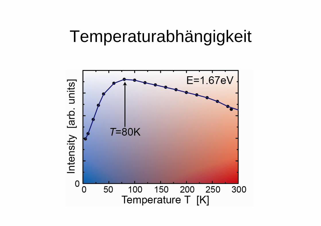
Temperaturabhängigkeit
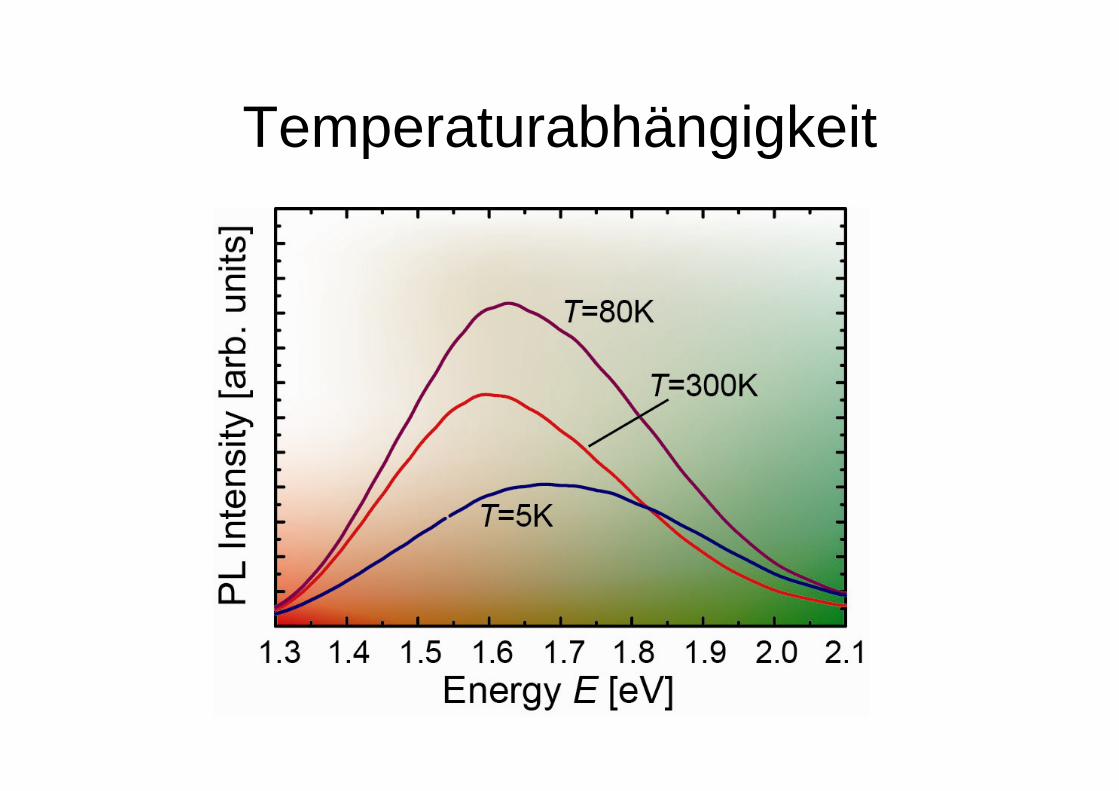
Temperaturabhängigkeit
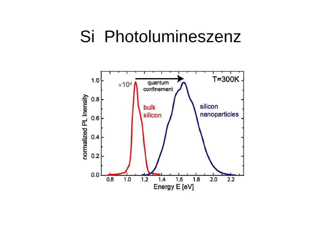
Si Photolumineszenz
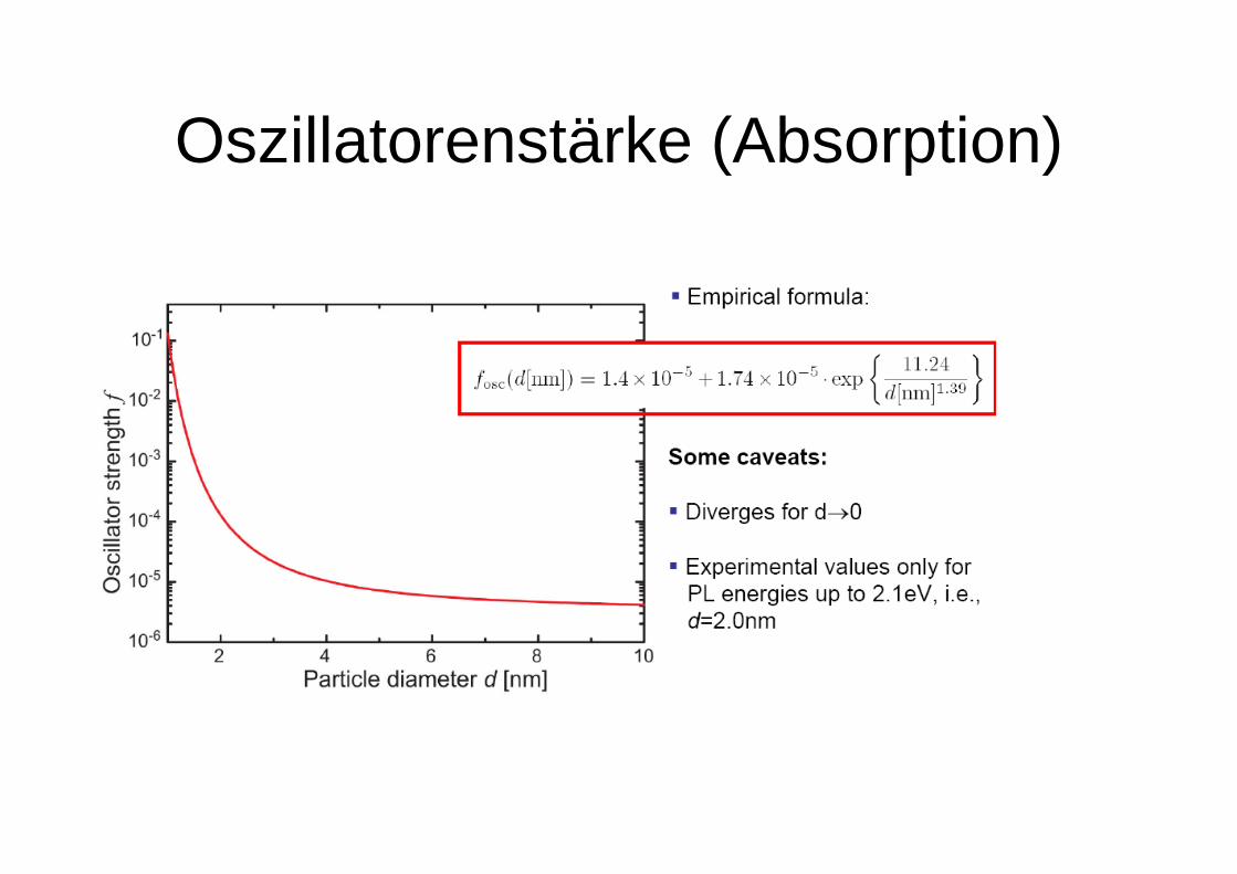
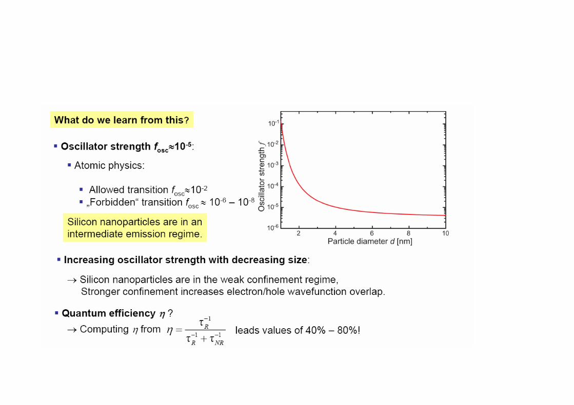
Oszillatorenstärke (Absorption)
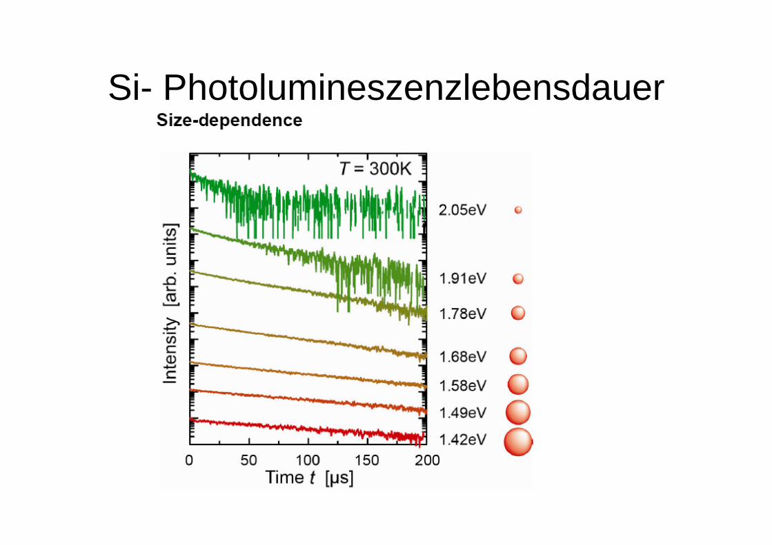
Si- Photolumineszenzlebensdauer
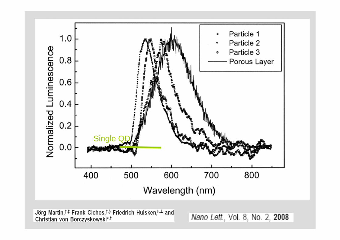
Single NC sSingle QD
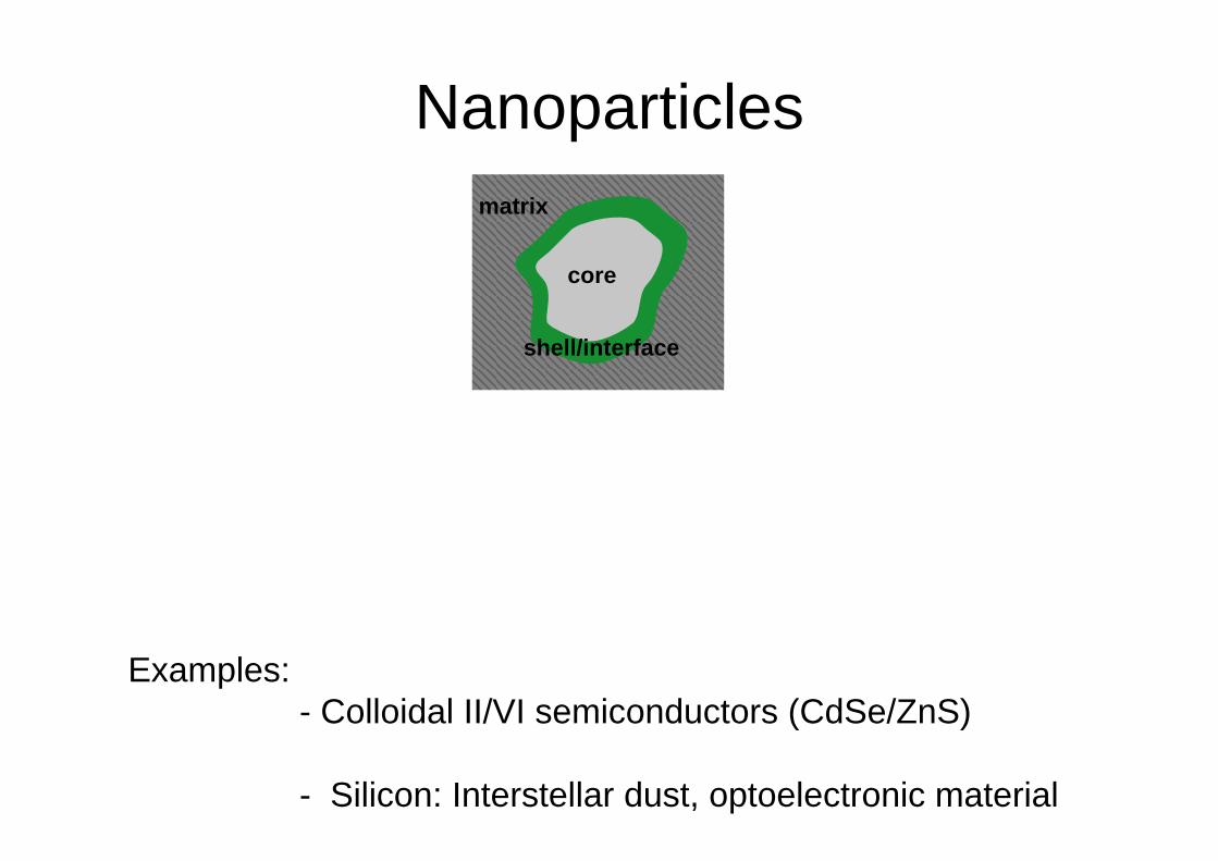
Nanoparticlesmatrix
core
shell/interface
Examples:- Colloidal II/VI semiconductors (CdSe/ZnS)
- Silicon: Interstellar dust, optoelectronic material
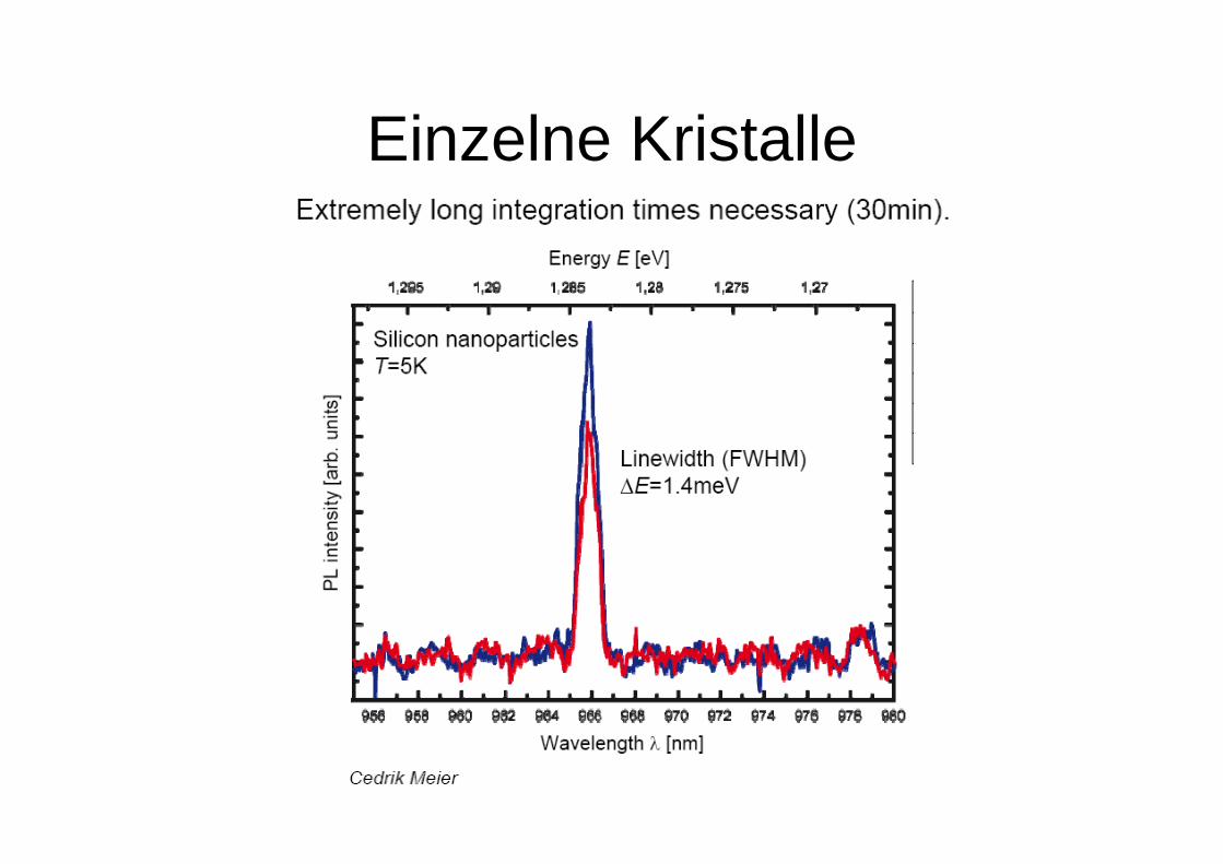
Einzelne Kristalle
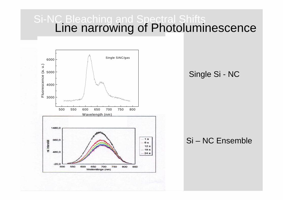
Si-NC Bleaching and Spectral Shifts
Single Si - NC
Si – NC Ensemble
Wavelength500 550 600 650 700 750 800
3000
4000
5000
6000 Single SiNC/gas
Flu
ores
cenc
e (a
. u.)
Wavelength (nm)
Line narrowing of Photoluminescence
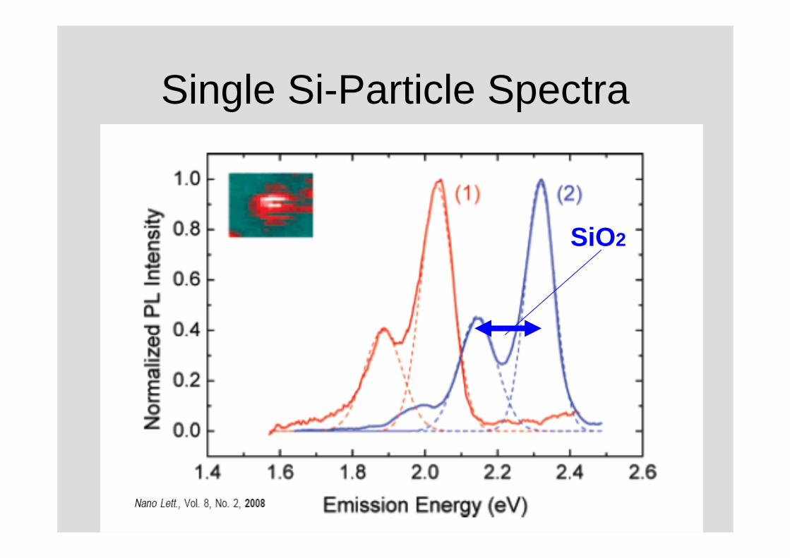
Single Si-Particle Spectra
SiO2
1,6 1,8 2,0 2,2 2,4
0
20
40
60
80
100
Obs
erva
tion
Tim
e (s
)
50
40
30
20
10
0Lum
ines
cenc
e (a
. u.)
Photon Energy (eV)
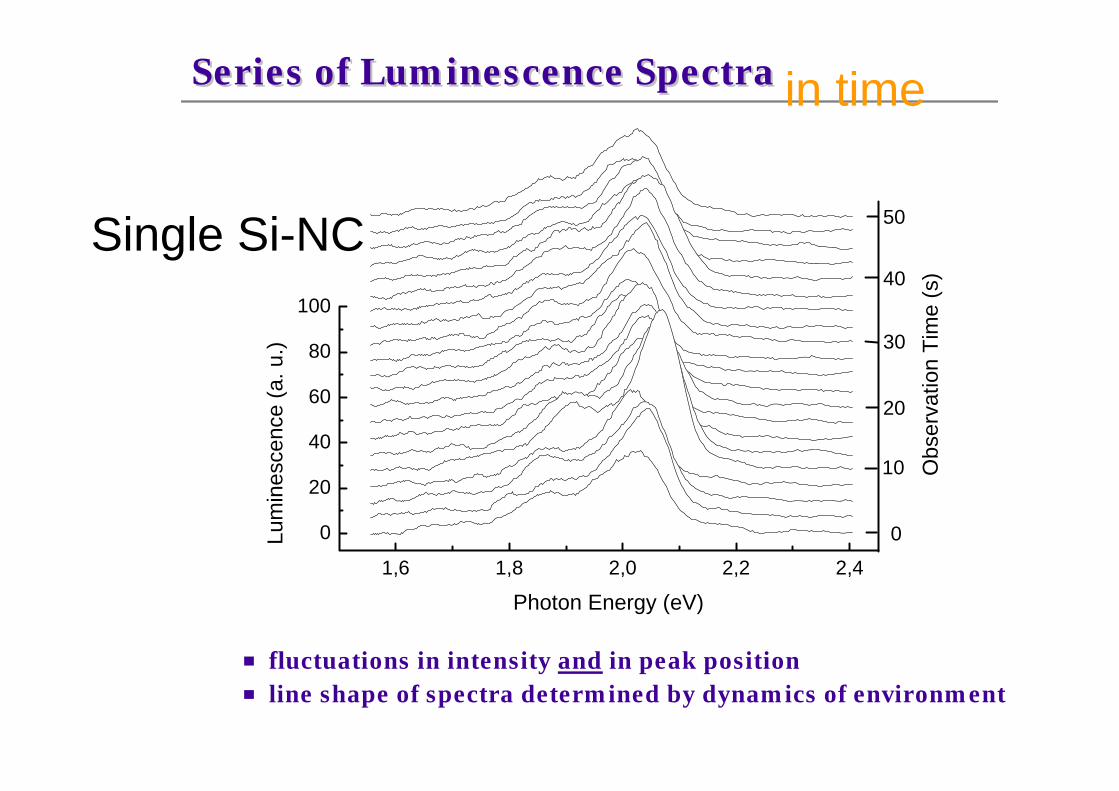
Series of Lum inescence SpectraSeries of Lum inescence Spectra
fluctuations in intensity and in peak positionline shape of spectra determ ined by dynam ics of environm ent
in time
Single Si-NC
Herstellungsmethoden
• Gasphasensynthese• Elektrochemisches Ätzen • Implantation• Lithographie
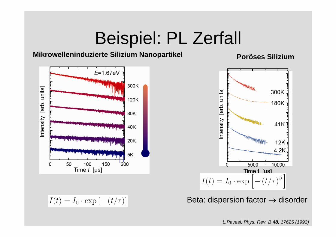
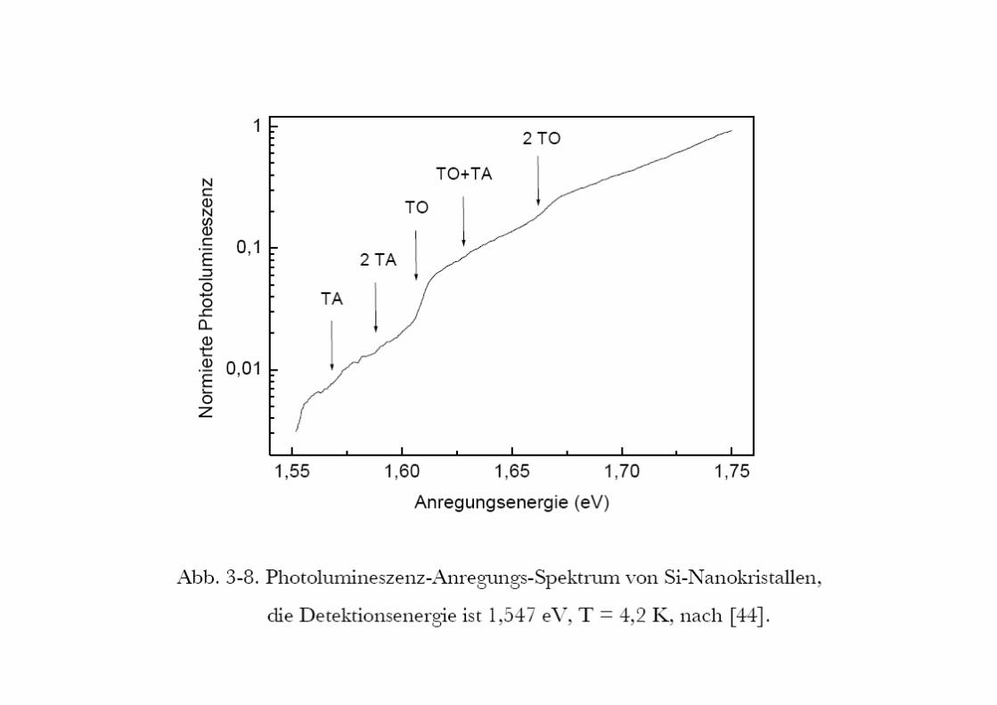
Beispiel: PL ZerfallPoröses SiliziumMikrowelleninduzierte Silizium Nanopartikel
L.Pavesi, Phys. Rev. B 48, 17625 (1993)
Beta: dispersion factor → disorder
Cedrik Meier Experimental Physics
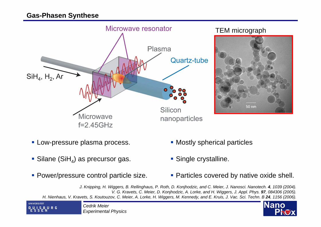
Gas-Phasen Synthese
J. Knipping, H. Wiggers, B. Rellinghaus, P. Roth, D. Konjhodzic, and C. Meier, J. Nanosci. Nanotech. 4, 1039 (2004).V. G. Kravets, C. Meier, D. Konjhodzic, A. Lorke, and H. Wiggers, J. Appl. Phys. 97, 084306 (2005).
H. Nienhaus, V. Kravets, S. Koutouzov, C. Meier, A. Lorke, H. Wiggers, M. Kennedy, and E. Kruis, J. Vac. Sci. Techn. B 24, 1156 (2006).
Low-pressure plasma process.
Silane (SiH4) as precursor gas.
Power/pressure control particle size.
TEM micrograph
Mostly spherical particles
Single crystalline.
Particles covered by native oxide shell.
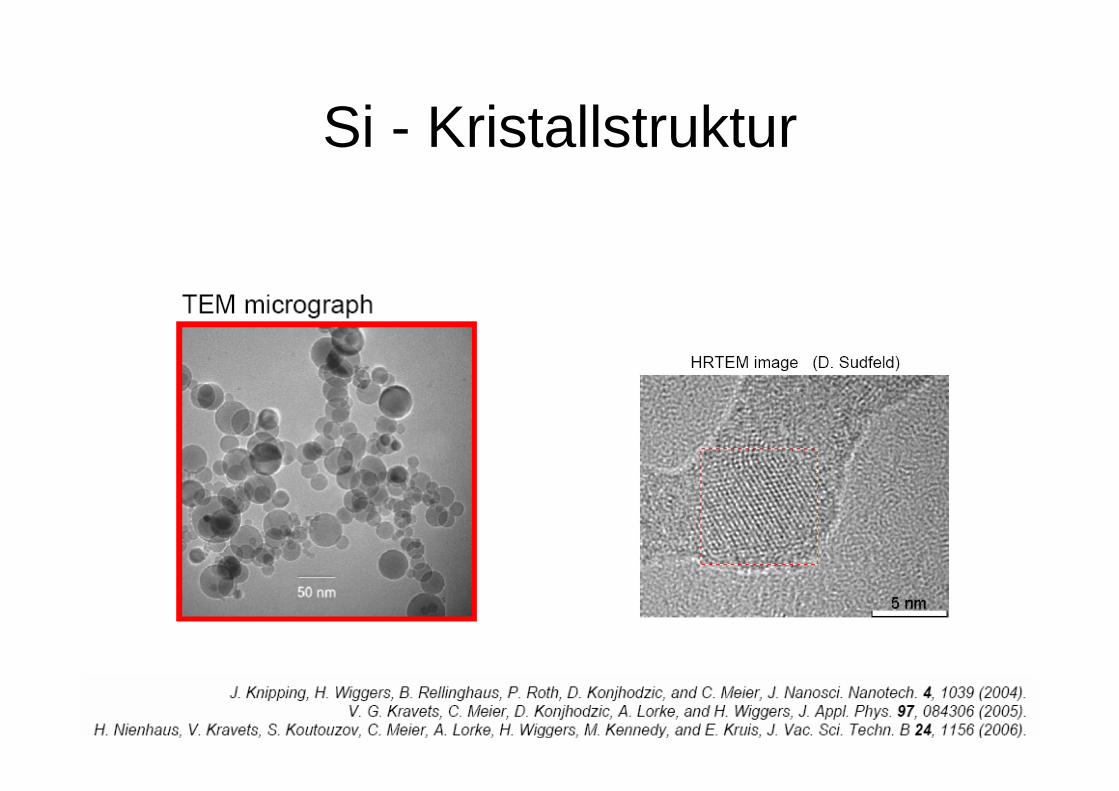
Si - Kristallstruktur
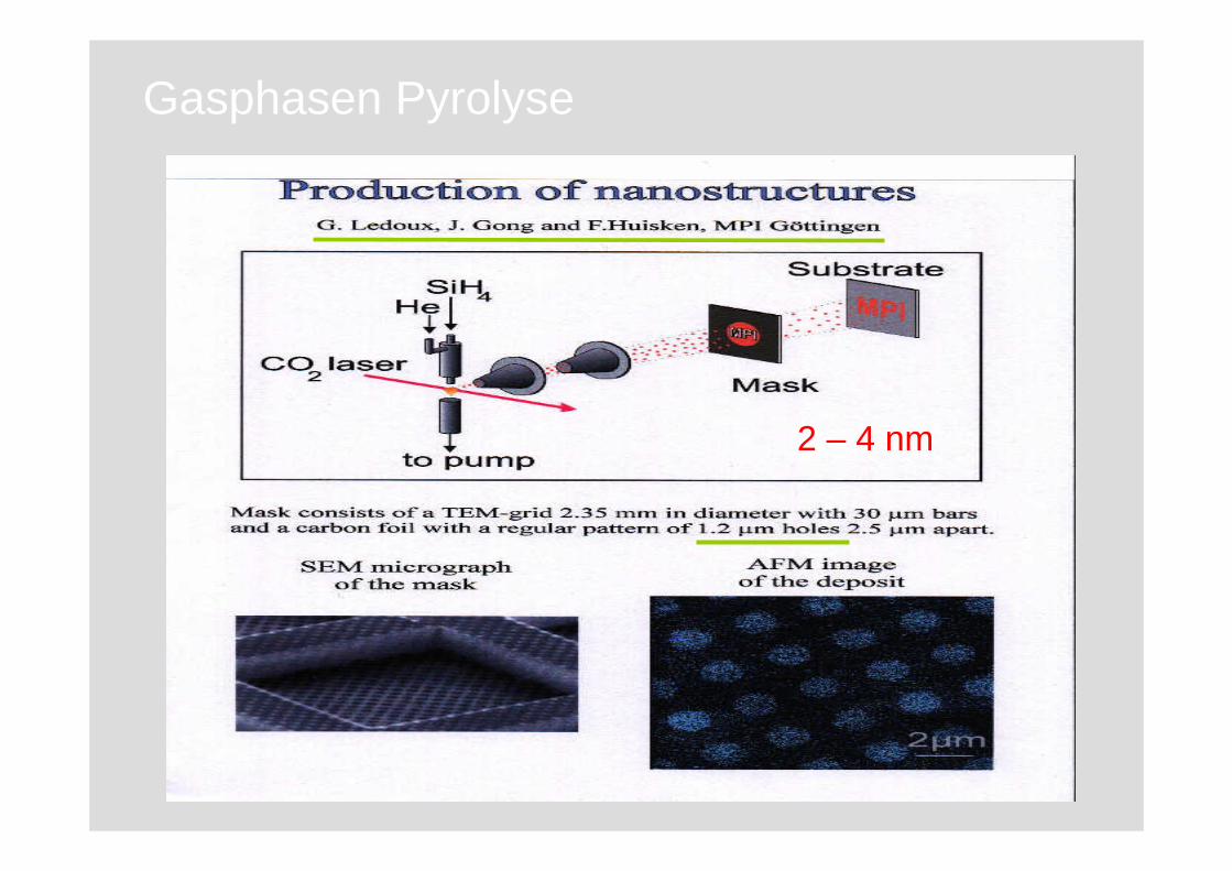
Gasphasen Pyrolyse
2 – 4 nm
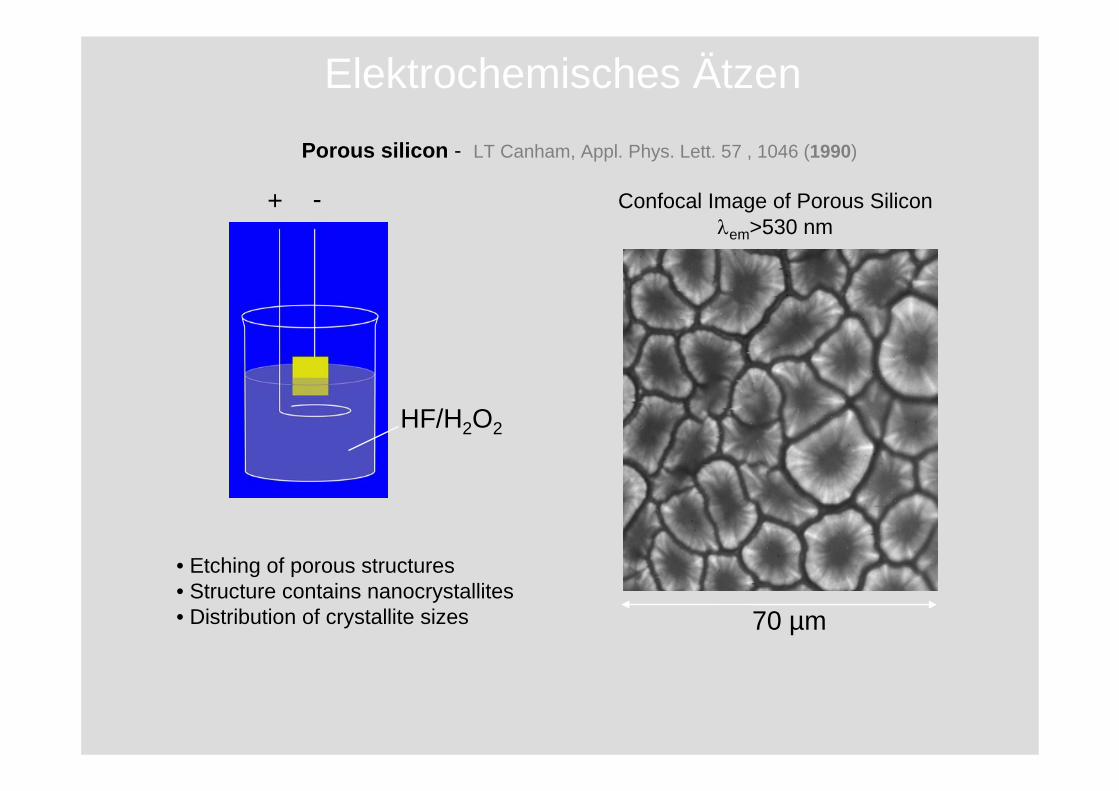
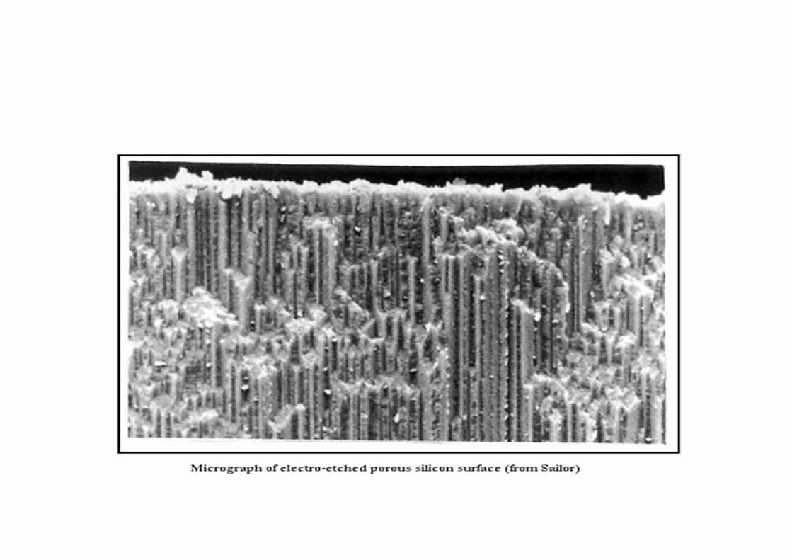
Elektrochemisches ÄtzenPorous silicon - LT Canham, Appl. Phys. Lett. 57 , 1046 (1990)
• Etching of porous structures• Structure contains nanocrystallites• Distribution of crystallite sizes 70 µm
+ - Confocal Image of Porous Siliconλem>530 nm
HF/H2O2
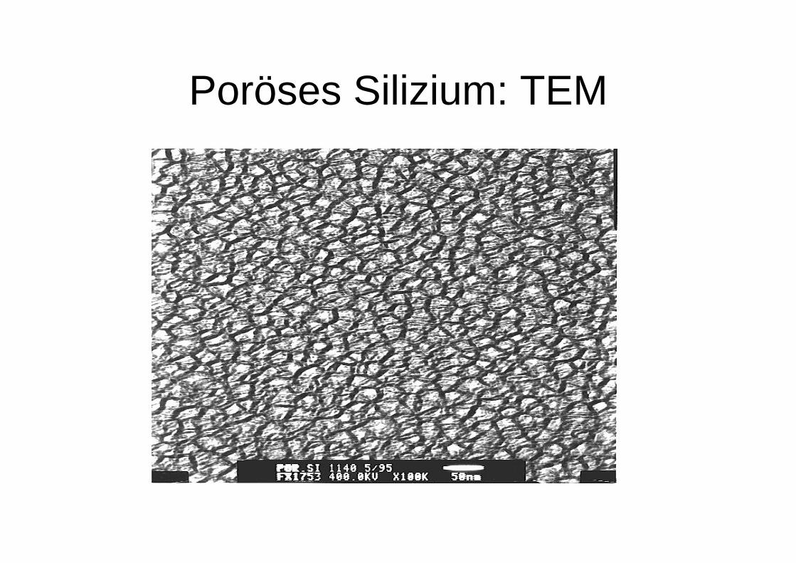
Poröses Silizium: TEM
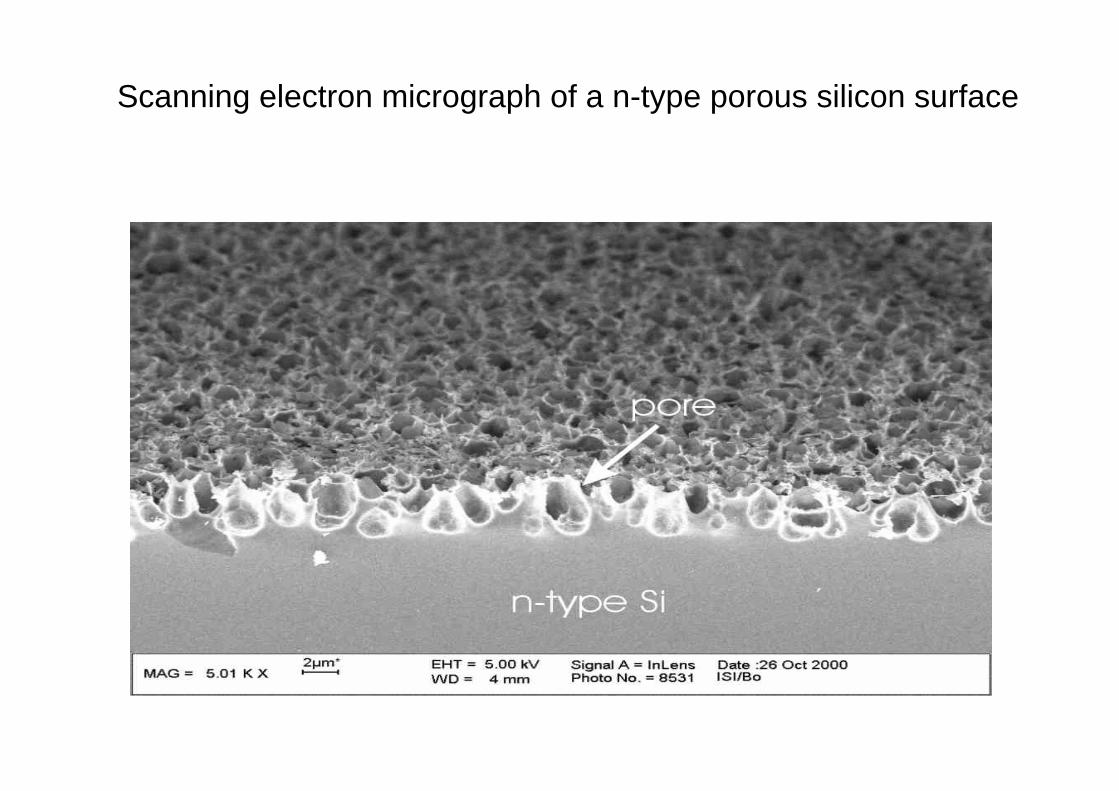
Scanning electron micrograph of a n-type porous silicon surface
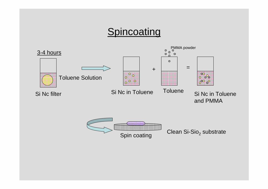
Spincoating
Si Nc filter
Toluene Solution
3-4 hours
Si Nc in Toluene
+
Toluene
PMMA powder
=
Si Nc in Tolueneand PMMA
Spin coating Clean Si-Sio2 substrate
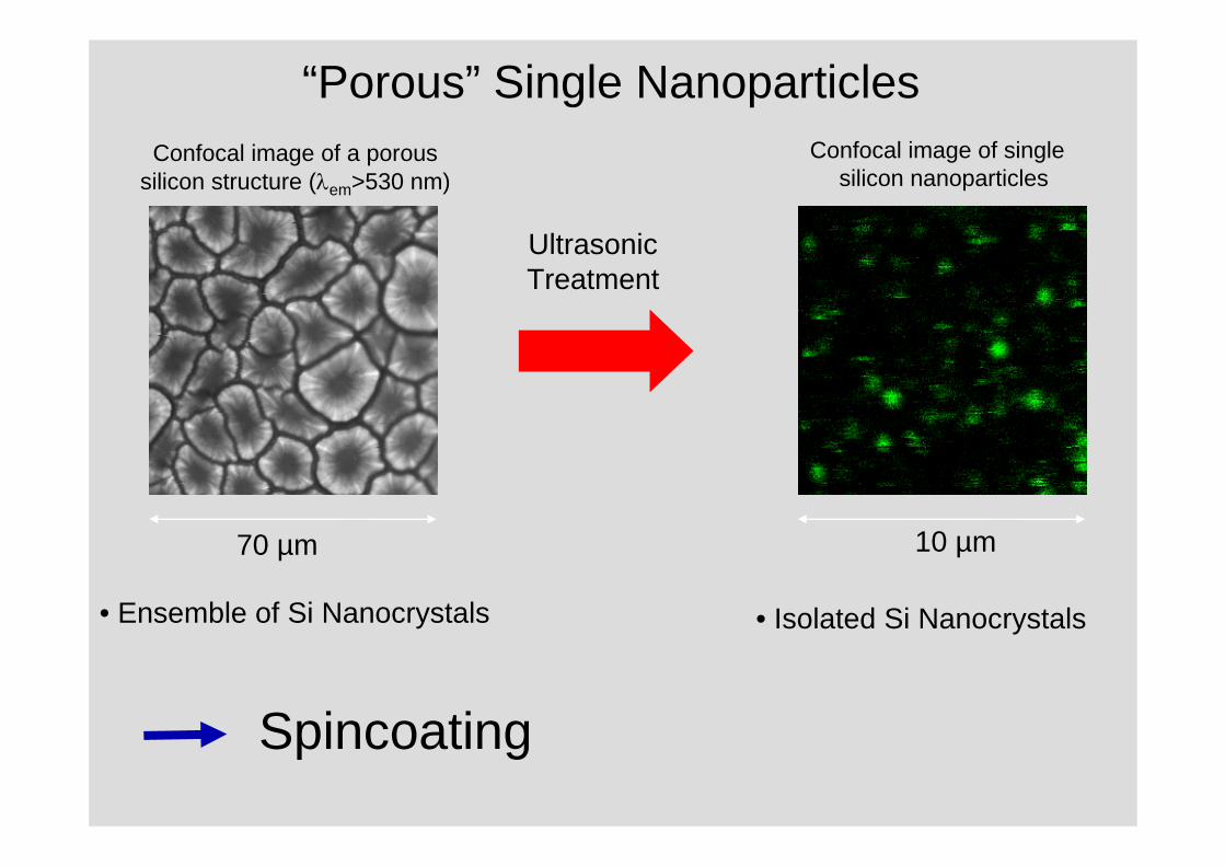
“Porous” Single NanoparticlesConfocal image of single
silicon nanoparticles
70 µm 10 µm
Confocal image of a poroussilicon structure (λem>530 nm)
UltrasonicTreatment
• Ensemble of Si Nanocrystals • Isolated Si Nanocrystals
Spincoating
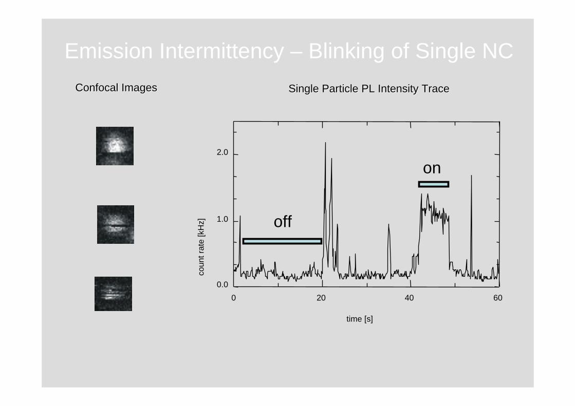
Emission Intermittency – Blinking of Single NC
0 20 40 600.0
1.0
2.0
time [s]
coun
t rat
e [k
Hz]
Single Particle PL Intensity TraceSingle Particle PL Intensity TraceConfocalConfocal ImagesImages
off
on
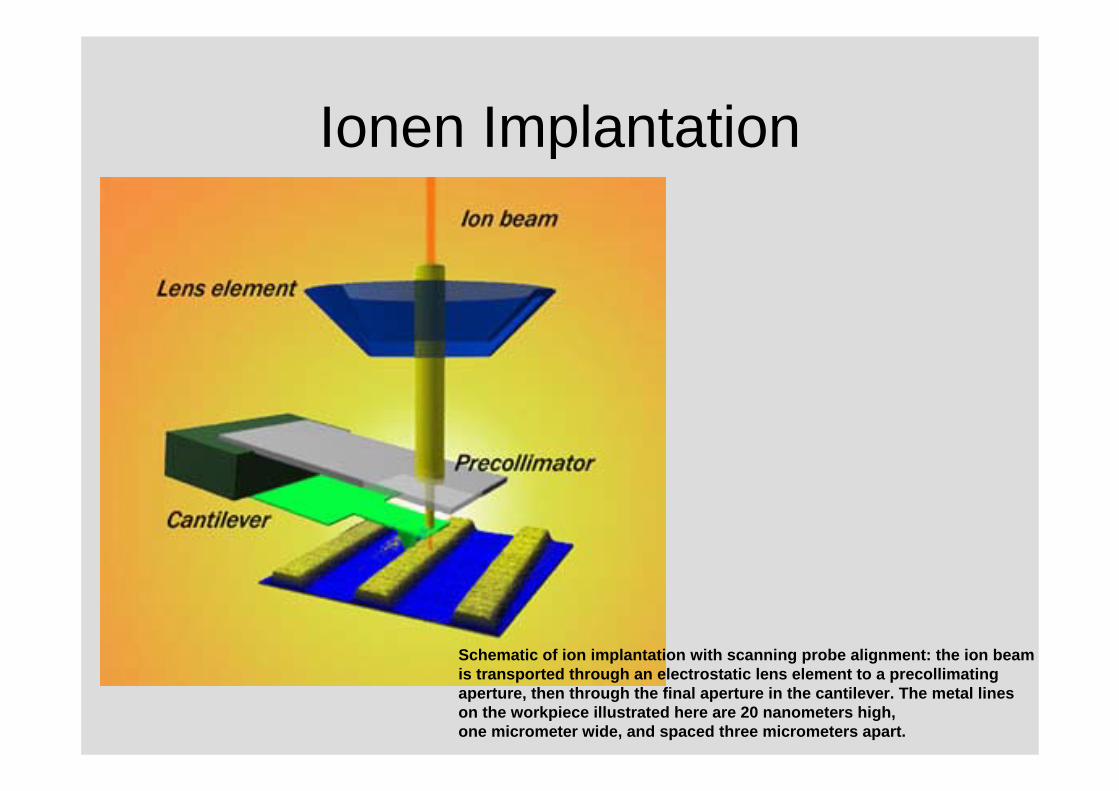
Ionen Implantation
Schematic of ion implantation with scanning probe alignment: the ion beamis transported through an electrostatic lens element to a precollimatingaperture, then through the final aperture in the cantilever. The metal lineson the workpiece illustrated here are 20 nanometers high, one micrometer wide, and spaced three micrometers apart.
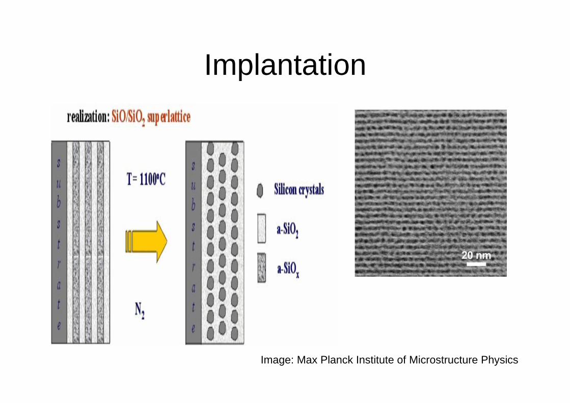
Implantation
Image: Max Planck Institute of Microstructure Physics
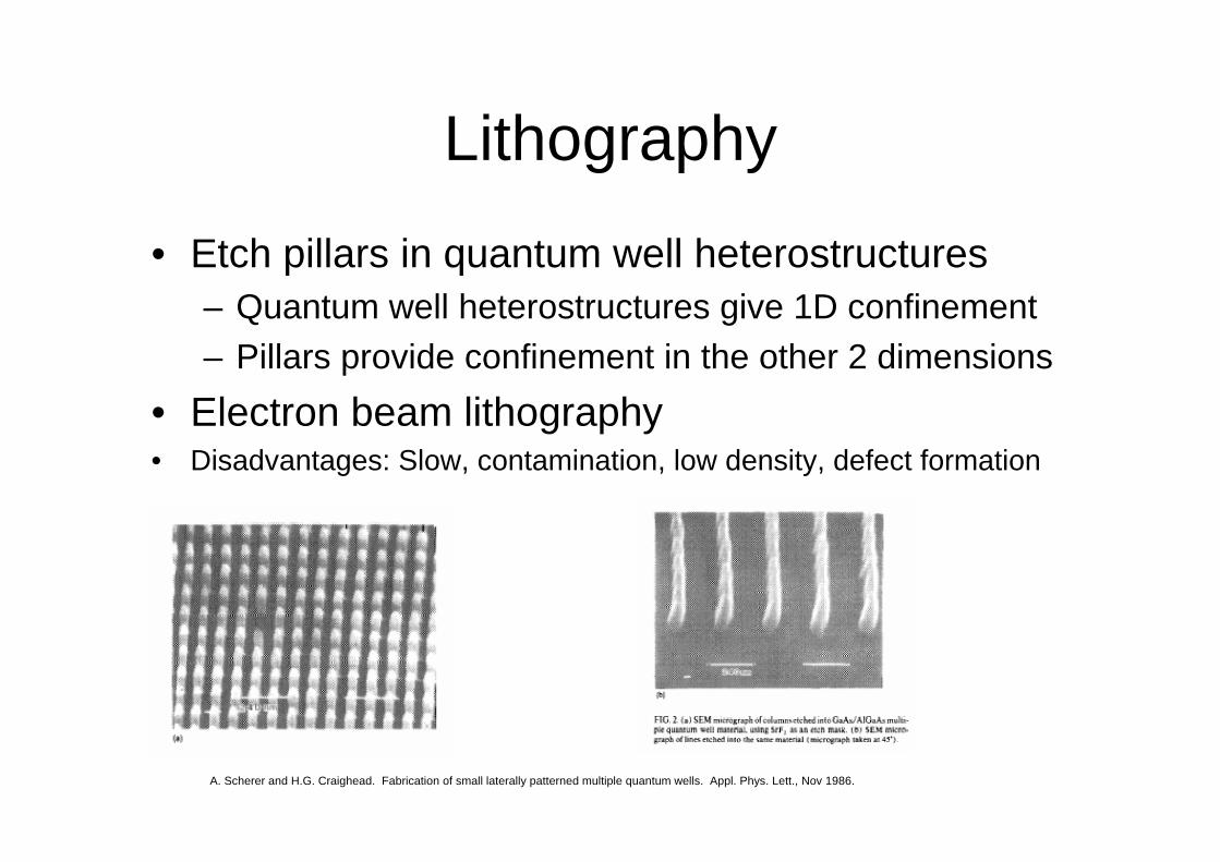
Lithography
• Etch pillars in quantum well heterostructures– Quantum well heterostructures give 1D confinement– Pillars provide confinement in the other 2 dimensions
• Electron beam lithography• Disadvantages: Slow, contamination, low density, defect formation
A. Scherer and H.G. Craighead. Fabrication of small laterally patterned multiple quantum wells. Appl. Phys. Lett., Nov 1986.
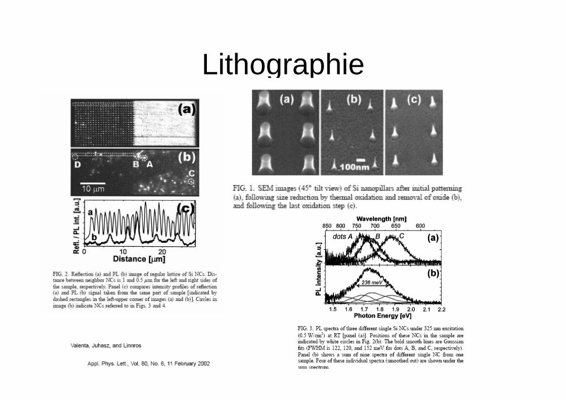
Lithographie
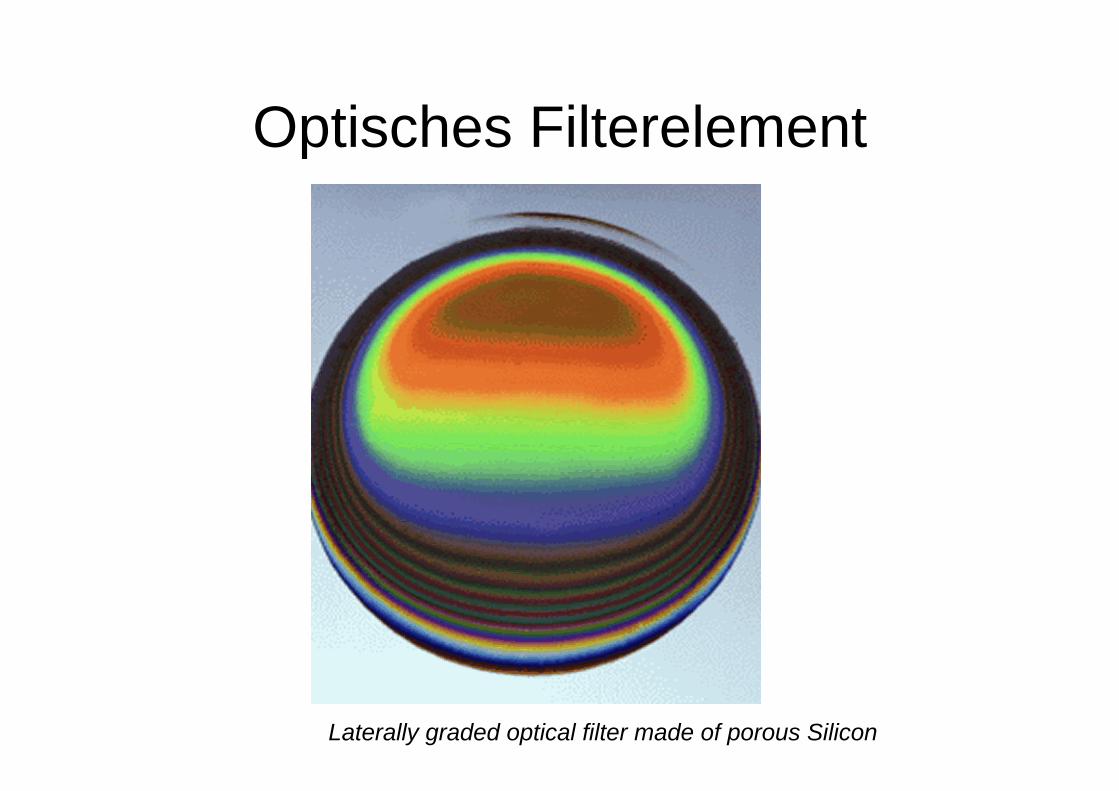
Optisches Filterelement
Laterally graded optical filter made of porous Silicon
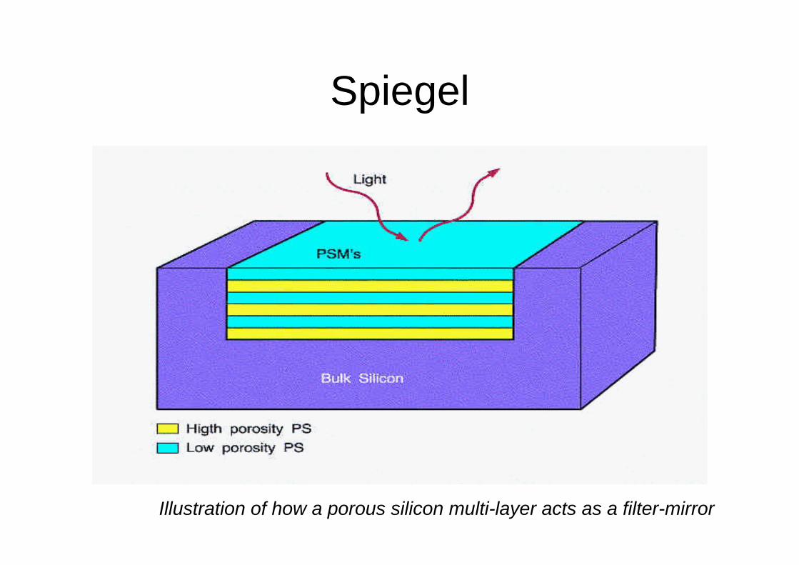
Spiegel
Illustration of how a porous silicon multi-layer acts as a filter-mirror
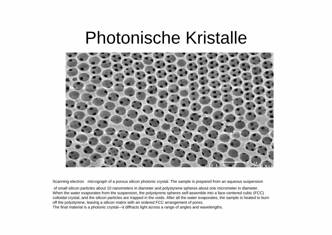
Photonische Kristalle
Scanning electron micrograph of a porous silicon photonic crystal. The sample is prepared from an aqueous suspension
of small silicon particles about 10 nanometers in diameter and polystyrene spheres about one micrometer in diameter. When the water evaporates from the suspension, the polystyrene spheres self-assemble into a face-centered cubic (FCC) colloidal crystal, and the silicon particles are trapped in the voids. After all the water evaporates, the sample is heated to burnoff the polystyrene, leaving a silicon matrix with an ordered FCC arrangement of pores. The final material is a photonic crystal—it diffracts light across a range of angles and wavelengths.
20 µm
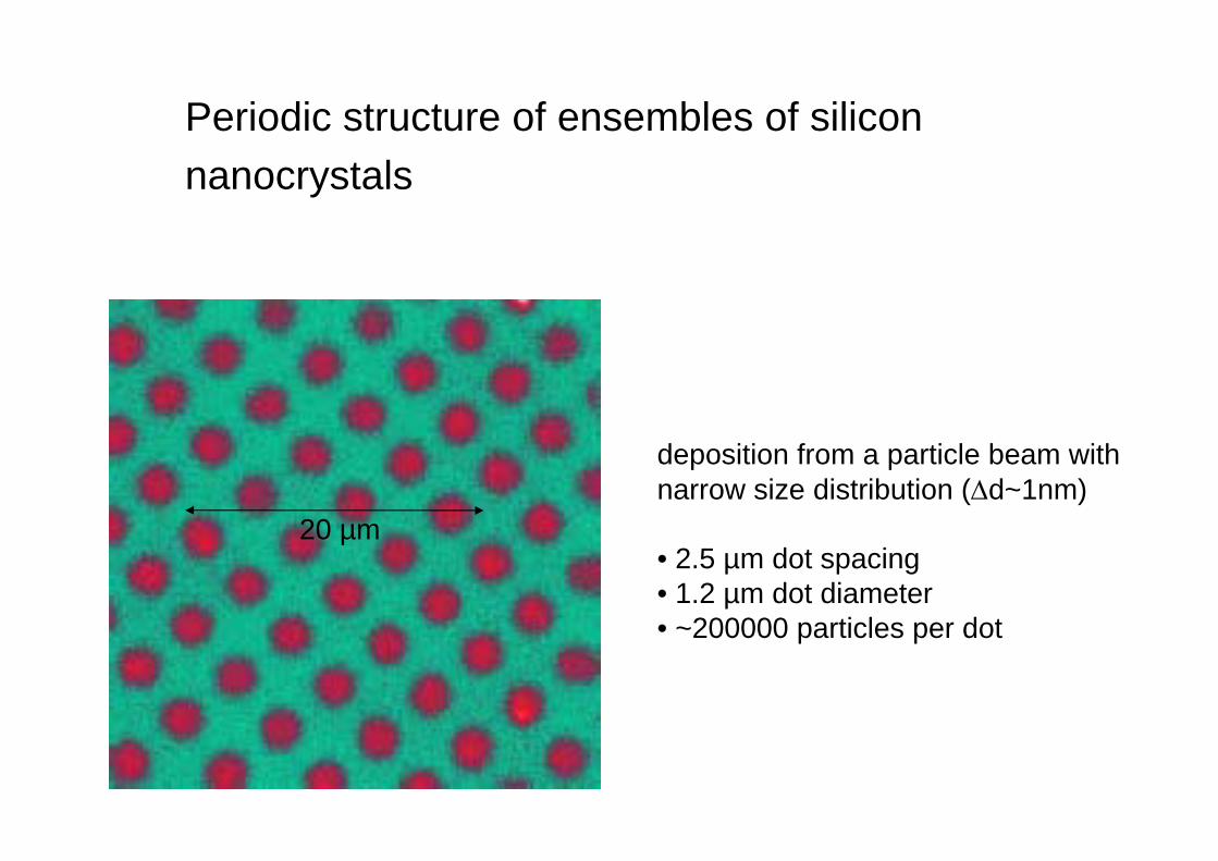
Periodic structure of ensembles of siliconnanocrystals
deposition from a particle beam withnarrow size distribution (Δd~1nm)
• 2.5 µm dot spacing• 1.2 µm dot diameter• ~200000 particles per dot
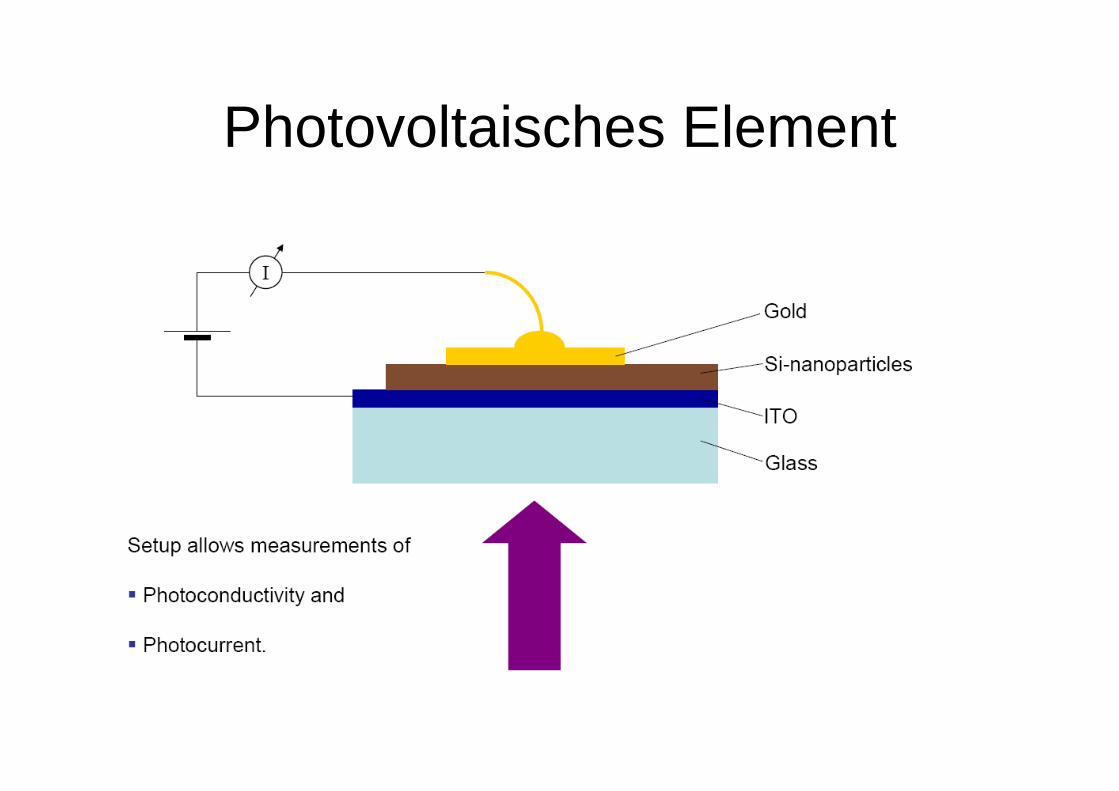
Photovoltaisches Element
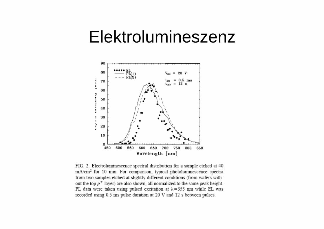
Elektrolumineszenz
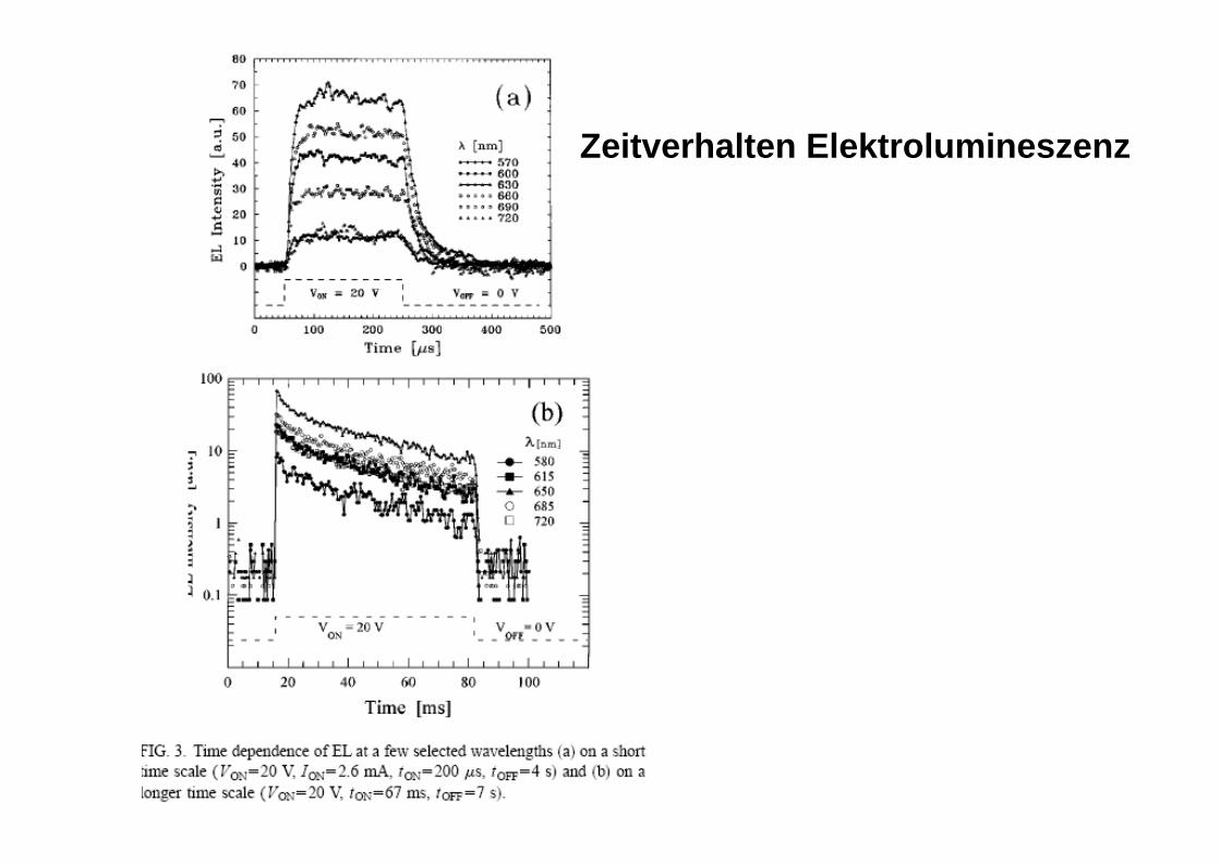
Zeitverhalten Elektrolumineszenz
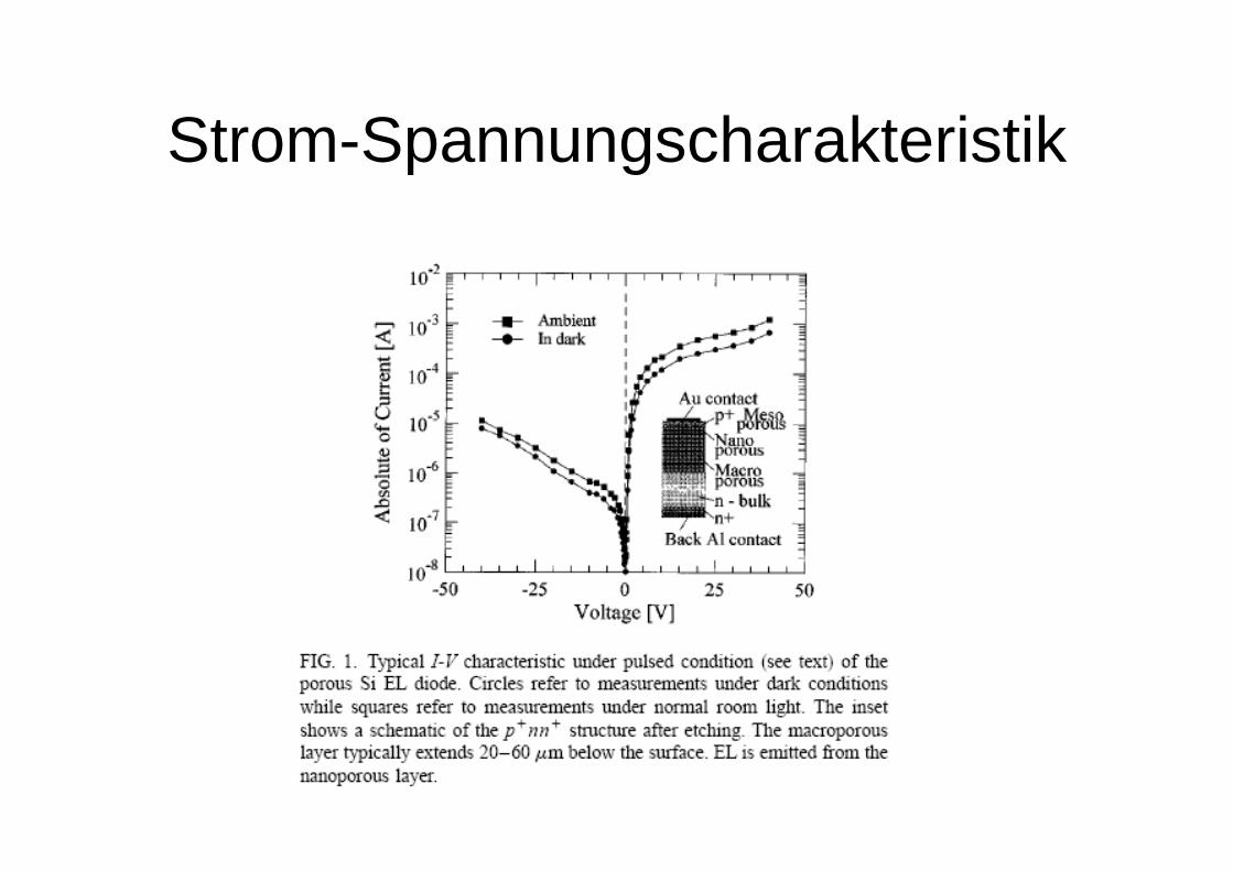
Strom-Spannungscharakteristik
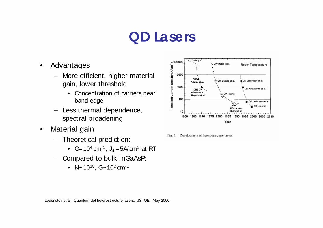
QD Lasers
• Advantages– More efficient, higher material
gain, lower threshold• Concentration of carriers near
band edge
– Less thermal dependence, spectral broadening
• Material gain – Theoretical prediction:
• G=104 cm-1, Jth=5A/cm2 at RT
– Compared to bulk InGaAsP:• N~1018, G~102 cm-1
Ledenstov et al. Quantum-dot heterostructure lasers. JSTQE, May 2000.