Embed Size (px)
Citation preview
Ultrathin gold nanowires for
transparent electronics
Dissertation
zur Erlangung des Grades
des Doktors der Ingenieurwissenschaften
der Naturwissenschaftlich-Technischen Fakultät
der Universität des Saarlandes
von
Johannes H. M. Maurer
Angefertigt am
INM ‒ Leibniz‒Institut für Neue Materialien
Saarbrücken
2017

Tag des Kolloquiums: 19.09.2017
Dekan: Prof. Dr. G. Kickelbick
1. Berichterstatter: Prof. Dr. T. Kraus
2. Berichterstatter: Prof. Dr. E. Arzt
Vorsitz: Prof. Dr. W. Possart
Akad. Mitarbeiter: Dr.-Ing. M. Zamanzade

„Der Sinn und das Kennzeichen echter
Wissenschaft besteht nach meiner Meinung
in den nützlichen Erfindungen, die man
daraus herleiten kann.“
Gottfried Wilhelm Leibniz

Publications and contribution report
This thesis has been published partially in four publications, which are referred to in the
text by their letter. The author declares his contributions to the publications included in
this thesis in the following.
(A) Sintering of Ultrathin Gold Nanowires for Transparent Electronics.
Maurer, J. H. M.; González-García, L.; Reiser, B.; Kanelidis, I.; Kraus, T.
ACS Appl. Mater. Interfaces 2015, 7, 7838–7842.
Contribution of Johannes H. M. Maurer: He designed the study and performed all
experiments. He conceived and wrote the manuscript.
(B) Ultrathin Gold Nanowires for Transparent Electronics: Soft Sintering and
Temperature Stability.
Maurer, J. H. M.; González-García, L.; Reiser, B.; Kanelidis, I.; Kraus, T.
Phys. Status Solidi (a) 2016, 213, 2336–2340.
Contribution of Johannes H. M. Maurer: He designed the study and performed all
experiments. He conceived and wrote the manuscript.
(C) Templated Self-Assembly of Ultrathin Gold Nanowires by Nanoimprinting
for Transparent Flexible Electronics.
Maurer, J. H. M.; González-García, L.; Reiser, B.; Kanelidis, I.; Kraus, T.
Nano Lett. 2016, 16, 2921–2925.
Contribution of Johannes H. M. Maurer: He designed the study and performed all
experiments. He conceived and wrote the manuscript.
(D) Direct nanoimprinting of a self-organizing nanowire ink for transparent,
flexible electronics.
Maurer, J. H. M.; González-García, L.; Backes, I. K.; Reiser, B.; Schlossberg, S.
M.; Kraus, T.
Adv. Mater. Technol. 2017, 1700034
Contribution of Johannes H. M. Maurer: He designed the study and performed
the printing experiments on PET and cling wrap. He designed the printing setup,
built the touch sensors, and characterized all the layers. He conceived and wrote
the manuscript.

Abstract
Transparent electrodes (TEs) are key components of modern optoelectronic devices like
touch screens, solar cells, and OLEDs, but an inherent trade-off between high electrical
conductivity and optical transparency limits the available material range. Indium tin
oxide (ITO) has been dominating the market, but cannot provide the mechanical flexi-
bility that novel devices based on polymer substrates require; high process temperatures
required for high-grade ITO exceed the thermal budget of many polymers. Solution-
processed metal grids from nanoscale building blocks are a promising alternative
providing superior mechanical flexibility at cost-effective and scalable fabrication with
low thermal budget.
For this dissertation, ultrathin gold nanowires (AuNWs) from wet-chemical synthesis
were explored as novel base material for TEs. Plasma sintering was shown to ameliorate
the wires’ high contact resistances and poor stability. A novel nanoimprinting process
was developed to pattern AuNWs into grids. The method relies on the large flexibility
of the AuNWs and their ability to self-assemble into continuous hierarchical superstruc-
tures in the cavities of a pre-patterned elastomeric stamp. The process yielded ordered
grids with submicron linewidth at low thermal budget, thus going beyond state-of-the-
art printed grids. The grids also showed competitive optoelectronic properties and supe-
rior mechanical flexibility to the incumbent materials and were applied as TEs in touch
sensors.

Zusammenfassung
Transparente Elektroden (TE) sind Schlüsselbauteile moderner optoelektronischer Gerä-
te wie Touchscreens, Solarzellen oder OLEDs. Es besteht jedoch ein intrinsischer Ziel-
konflikt zwischen elektrischer Leitfähigkeit und optischer Transparenz, was die Aus-
wahl an verfügbaren Materialien stark eingrenzt. Indium-Zinn-Oxid (ITO), welches bis
heute den Markt dominiert, kann die mechanische Flexibilität neuer Geräte basierend
auf Polymersubstraten nicht gewährleisten; die für hochwertiges ITO benötigten Pro-
zesstemperaturen übersteigen oft die thermische Beständigkeit vieler Polymere. Nassbe-
schichtete Metallgitter aus nanoskaligen Bausteinen sind eine vielversprechende Alter-
native: sie weisen höhere mechanische Flexibilität auf und können durch kosteneffizien-
te und skalierbare Prozesse bei niedrigen Temperaturen hergestellt werden.
In der vorliegenden Dissertation wurden ultradünne Gold Nanodrähte (AuNWs) aus
nasschemischer Synthese als neuartige Bausteine für TE untersucht. Durch Plasmasin-
tern konnten die hohen Kontaktwiderstände und geringe Stabilität der AuNWs verbes-
sert werden. Ein neuartiger Nanopräge-Prozess wurde entwickelt, um AuNWs zu Git-
tern zu strukturieren. Die Methode beruht auf der hohen Flexibilität der AuNWs und
deren Fähigkeit sich zu kontinuierlichen, hierarchischen Überstrukturen in den Zwi-
schenräumen eines vorstrukturierten Stempels selbst anzuordnen. Mit dem Prozess
wurden geordnete Gitter mit Linienbreiten unter einem Mikrometer unter geringer
thermischer Einwirkung hergestellt. Die Gitter haben konkurrenzfähige optoelektroni-
sche Eigenschaften zu den vorherrschenden Materialien bei überlegener mechanischer
Flexibilität und wurden als TE in berührungsempfindlichen Sensoren verbaut.

Acknowledgements
First of all, I am very grateful to my “Doktorvater” Prof. Tobias Kraus, genius scientist,
polymath, and gourmet, who always kept the right balance between colleague and boss
creating a pleasant and productive working atmosphere during the entire time. Thank
you very much for giving me the opportunity to write my dissertation in the “structure
formation group” and your valuable guidance and advices during the last three years.
Thank you for the generous support of international conferences and workshops, which
should not be taken for granted.
I am grateful to Prof. Eduard Arzt for giving me the opportunity to write my disserta-
tion at the INM and the willingness to act as second reviewer. Prof. Arzt was a constant
companion of my career as material scientist starting with his lecture slides that laid the
fundamentals of materials science during my Bachelor studies in Stuttgart, as official
supervisor of my master thesis, and now as reviewer of my dissertation. Thank you very
much for your support.
Many thanks go to my “scientific advisor” PD Dr.-Ing. Guido Falk, head of the re-
search group of structural and functional ceramic at Saarland University, for the various
pleasant scientific discussions during my PhD.
Special thanks go to the “Nanospekt” project team, better known as “Nanospekt fami-
ly”, which expresses to me much better the close relation and friendship we have devel-
oped during the last 3 years. I think we were a great team of scientists, office mates, and
friends: First of all, the “mother”, Dr. Lola González-García, supervisor, mentor, and
friend with the genius nose for the right (publication) story. Without her, I would not
have been able to write the thesis the way it is now. Thank you very much for guiding
me during my thesis, your help with the Rhino 3D figures, and the energized discus-
sions about science and many other topics…;-). Thanks also for teaching me the most
important expressions in Spanish ;-). The “father” Dr. Ioannis Kanelidis, “Kanela”, “lab
president” and best “Kritharaki” cook. Thanks for your help with the wire synthesis, the
Raman measurements and the epic “Kanelidis mix” that facilitated every lab cleaning.
The “sister” Beate (Haas) Reiser, co-PhD student in the project, who shared with me
the good and bad days of a life as PhD student. Her work on the synthesis laid the foun-
dations of the work on AuNWs. Thank you for your help and chemistry advices.
Sebastian Beck, “BeckNorris”, the engineer in our team, multi-talented problem-solver
and huge Globus-Fleischkäsweck-Fan ;). Thanks for your help with the nanoimprinting
setup and the CAPA tool.
Many thanks go to the master students and student assistants of “Team Nanospekt” who
directly contributed to the work for this thesis: Indra Backes, who helped with incredi-
ble enthusiasm in the scale-up of the imprinting process during her master thesis; Sarah
Schlossberg, exchange student from UCSD, who advanced the printing on flexible sub-
strates; Manuel Hawner for his help with the molding of the PDMS stamp.
Many thanks go to the rest of the structure formation group. I think we had an amazing
working atmosphere and we were a great mixture of outstanding characters: Gabi
Koster, secretary and “mother” of the group, efficient, competent and unbelievably nice.
Thanks for perfect organization of the group and your constantly positive charisma.
Many thanks go to my colleagues as PhD students: Dr. Dominik Gerstner, “Dojo G”,
already graduated, SAXS expert and great fan of steak haché and artificial banana fla-
vor. Thanks for your help with analyzing SAXS data and for great time at the synchro-
tron (still jealous of Nina’s lunch bag). Aljosha Rakim-Jochem, “de Chef”, awesome
chemist and passionate delegator ;-). Thanks for many valuable discussions about sci-
ence and life, but also for great “nonsense talk” in the lab that made hard days in the lab
more enjoyable. Thomas Kister, “Supraman”, the perfect fusion of Bud Spencer and
MacGyver, genius doer that can synthesize particles with vanishingly small polydisper-
sity and any ligand you want. He is the guy you should call if you have any prob-
lems…he will fix it with Epoxy glue. Andreas Hegetschweiler, the “Swiss Saarlandian”,
constantly trying to kid each other, which made the work days always more fun. Thanks
for taking over the exam corrections. Juraj Drzic, “J”, the new PhD student in the Nan-
ospekt project and office mate. Robert Strahl, “engineer 2.0” in the Nanospekt team,
thanks for your help with various engineering tasks. Many thanks go to our lab techni-
cians: Anika Kleemann, “lab dragon” or “lab mum”, but definitely “lab head” and group
organizer. I don’t want to imagine how the labs would have looked like without your
constant care. Thank you very much for your help synthesizing gold acid and particles.
The same holds for Nicole Schiff and Kathrin Alt. Thank you very much for your help in
the lab, the ordering of chemicals and your constant smile . Many thanks go also to:
Dr. Daniel Brodoceanu, the “laser guy”; thank you for many inspiring conversations in
the lab (if you talk 10 min with him, you will have more ideas than you can ever im-
plement). Dr. Genesis Ankah, “The FIBber”; thanks for your help sputtering electrodes
in the FIB. Dr. David Doblas-Jiménez, Dr. Peng Zhang, Dr. Thibaut Thai, Dr. Manuel
Oliva, Dr. Alberto Escudero, Dr. Vikrant Naik, Anna Zimmermann, Jonas Hubertus,
Jona Engel, Anna Heib, Christopher Scherrer, Andrea Pyttlik, Lars-Arne Meyer, Lukas
Engel and Thilo Grammes for the nice times together in the lab.
Many thanks go to: Diana Löb and Silvia de Graaf, the secretaries of Prof. Arzt, for the
perfect PhD administration; Dr. Sabine Heusing, the “queen” of the UV-Vis, for her
help with the optical characterization; Dr. Thiago Martins Amaral for his help with the
setup for the capacitive touch screen; Jenny Kampka for providing the PET foil; Sarah
Fischer for helping with the PDMS stamps; Dr. Marcus Koch for his help with SEM
analysis; Dr. Johanna Blass, Dr. Arzu Colak, and Marius Gipperich for their help with
the AFM analysis; Simon Fleischmann for his help with the Raman measurements; Mir-
iam Badziong for great bookings of the business trips.
I am very grateful to Dr. Heiko Wolf and Songbo Ni from IBM Research – Zurich for
the warm welcome and great weeks of creative research and fun during my visit at the
IBM laboratories. Many thanks go to the DAAD and the “GradUS global” program of
the Saarland University for the funding of the visit.
Many thanks go to my friends that were constantly “available” to overcome a frustrating
lab day with “a beer from my hometown” and the awesome “Spaghetti Nauwies” in the
eponymus bistro. I am certainly going to miss the WhatsApp-message: “11:30 Mensa?”
I am particularly grateful to my parents. Thank you for unlimited support during the last
29 years!!! I am grateful also to my sister Christine who has always shared the thrill
with me, if a paper was going to be accepted or not. Thanks for the epic “evil eatings”
after each publication ;-).
There are no proper words to describe the deepest gratitude I owe to my wife Isabelle
who continuously managed to make me laugh and feel happy even at days when every-
thing failed in the lab. THANK YOU!

Table of contents
1 INTRODUCTION AND MOTIVATION.............................................................. 1
2 THEORY AND STATE OF THE ART ................................................................. 5
2.1 Transparent electrodes ...................................................................................... 5
2.1.1 Modern applications and requirements .............................................. 5
2.1.2 Transparency-conductivity trade-off ................................................ 10
2.1.3 Transparent conductive oxides ......................................................... 11
2.1.4 Solution-based transparent electrodes for flexible devices .............. 12
2.1.4.1 Random metal nanowire networks ................................................... 14
2.1.4.2 Ordered metal grids .......................................................................... 16
2.2 Patterning of nanoparticle inks for electronics ............................................... 19
2.2.1 Fabrication of transparent metal grids from nanoparticle inks ........ 19
2.2.2 Direct nanoimprinting of nanoparticles ........................................... 22
2.3 Sintering of nanoparticle inks for electronics ................................................ 26
2.3.1 Photonic sintering ............................................................................ 27
2.3.2 Chemical sintering ........................................................................... 29
2.3.3 Plasma sintering ............................................................................... 30
2.4 Ultrathin gold nanowires (AuNWs) ............................................................... 32
2.4.1 Synthesis and growth mechanism .................................................... 32
2.4.2 Self-assembly ................................................................................... 36
2.4.3 AuNWs for transparent electronics .................................................. 36
3 RESULTS ............................................................................................................... 39
3.1 Publication A: Sintering of Ultrathin Gold Nanowires for Transparent
Electronics. ..................................................................................................... 39
3.2 Publication B: Ultrathin Gold Nanowires for Transparent Electronics: Soft
Sintering and Temperature Stability. .............................................................. 41
3.3 Publication C: Templated Self-Assembly of Ultrathin Gold Nanowires by
Nanoimprinting for Transparent Flexible Electronics. ................................... 43
3.4 Publication D: Direct Nanoimprinting of a Colloidal Self-organizing
Nanowire Ink for Transparent, Flexible Electronics. ..................................... 45
4 DISCUSSION ......................................................................................................... 47
4.1 Sintering of AuNWs ....................................................................................... 47
4.2 Patterning of AuNWs ..................................................................................... 50
5 CONCLUSIONS .................................................................................................... 53
6 OUTLOOK ............................................................................................................. 55
7 BIBLIOGRAPHY .................................................................................................. 57
8 APPENDIX ............................................................................................................. 69
8.1 List of abbreviations and symbols .................................................................. 69
8.2 Sheet resistance ............................................................................................... 71
8.3 List of publications ......................................................................................... 72
8.4 Conference contributions ................................................................................ 73
1 Introduction and motivation
- 1 -
1 Introduction and motivation
Since the first iPhone was introduced in 2007 by Apple, smartphones have become an
integral part of our daily life. A recent study in the United Kingdom revealed that we
spend on average 3 hours and 16 minutes per day with our smartphone.1 An essential
component for the human-machine interaction is the touch-sensitive display, which acts
as user interface in many other devices, too, including tablets, e-book readers, or car
entertainment systems. Integral parts of the touch screens are “transparent electrodes”:
materials that conduct electricity, but are at the same time transparent to visible light.2
Such materials are also prerequisites for the functionality of numerous other optoelec-
tronic devices such as organic light-emitting diodes and solar cells (section 2.1.1).
The range of available materials that combine high optical transparency and good elec-
trical conductivity is limited because both properties are connected: materials with good
electrical conductivity like metals, for instance, are usually opaque in bulk state because
high carrier concentrations imply strong optical absorption (section 2.1.2). Doped metal
oxides represent a unique class of materials that combine transparency and conductivity.
In particular, tin-doped indium oxide (ITO) evolved into the predominantly used mate-
rial for transparent electrodes today (section 2.1.3).3
The trend towards flexible and organic devices based on polymer substrates sets new
challenges: foldable displays, wearable touch screens, and bendable solar cells require
transparent electrodes to be mechanically flexible, and their fabrication must not exceed
the thermal budget of polymer substrate. ITO and other transparent oxides do not meet
these requirements due to their ceramic brittleness and the often high process tempera-
tures. Many alternatives to ITO have been proposed including conductive polymers,
carbon materials, and metal grids, among others (section 2.1.4). Bottom-up fabrication,
where conductive nanostructures (e.g. metal nanoparticles) get deposited from liquid
dispersions (“inks”) have been reported as a promising approach: solution-processing
allows for cost-effective and scalable fabrication at low thermal budget; additive deposi-
tion of particles reduces the required amount of material.4 In particular, random metal
1 Introduction and motivation
- 2 -
nanowire networks (section 2.1.4.1) and ordered metal grids (section 2.1.4.2) made
from nanoscale building blocks are potential competitors for ITO, combining high elec-
trical conductivity, optical transparency, and mechanical flexibility.5
Bottom-up fabrication of electronic features from metal nanoparticle inks usually in-
volves two steps:
(1) Controlled deposition of the particles: Precise patterning is important for device per-
formance, but deterministic assembly of individual particles is challenging due to their
nanometer-size. Novel methods have been developed to precisely deposit conductive
patterns from nanoparticle inks following the concepts of traditional printing (“printed
electronics”) (section 2.2).
(2) Sintering to reduce contact resistances: After synthesis, nanoparticles are generally
capped by organic molecules, which lend them the necessary colloidal stability in dis-
persion, but at the same time provoke high contact resistances between individual nano-
particles. Hence, nanoparticle layers usually have to be annealed after deposition to re-
move the ligands or modify them (section 2.3).
Today’s inks prevalently consist of spherical metal nanoparticles that provide high par-
ticle mobility and good printability. Anisotropic particles with high aspect ratios could
ease percolation and reduce the number of insulating junctions at particle-particle inter-
faces. Stiff wires impede printing, however. Commercially available silver nanowires,
for instance, are usually randomly dispensed to form networks like “pick-up sticks”,
which provides only little control over the network geometry.
Ultrathin gold nanowires (AuNWs) that have recently become available from wet-
chemical synthesis are an alternative base material: they combine ultra-high aspect rati-
os (> 1000) with high particle mobility and mechanical flexibility through their small
diameter (< 2 nm) (section 2.4). The initial publications on AuNW thin-films showed
their ability to form highly transparent thin films, but insulating oleylamine ligand shell
caused high contact resistances between the individual wires; sheet resistances in the
MΩ range were reported. Their small diameter makes them susceptible to fragmentation
by the Rayleigh instability, too.

1 Introduction and motivation
- 3 -
In this thesis, I explore the use of AuNWs as building blocks for the fabrication of
transparent electrodes addressing the two steps for bottom-up fabrication:
(1) Sintering to reduce contact resistances between wires and increase the stability of
AuNW thin films (publications A and B).
(2) Patterning of the wires into high resolution metal grids (publications C and D).

2 Theory and state of the art
- 5 -
2 Theory and state of the art
2.1 Transparent electrodesa
Early scientific reports on ultrathin transparent and conductive metal films can be found
at the end of the 19th
century.6 Applications of transparent electrodes (TEs) appeared
first with the advent of the electronics industry during World War II. Transparent con-
ductive oxides were used as transparent heaters for the de-icing of cockpit windows.3 In
the following centuries, consumer electronics and energy applications stimulated the
research on TEs with the emergence of flat-panel display technology and solar cells.
Doped oxides, particularly ITO, were shown to uniquely combine transparency and
conductivity and became the leading material. In the last decades, TE development has
been fueled by the growing market of modern optoelectronic applications like
smartphones, smart TVs, thin-film organic solar cells, and large-area organic lighting.2
Novel solution-based TEs are challenging the incumbent ITO that struggles with the
requirements of future flexible, polymer-based devices.
2.1.1 Modern applications and requirements
In this section, the role of TEs in the four most relevant modern optoelectronic devices
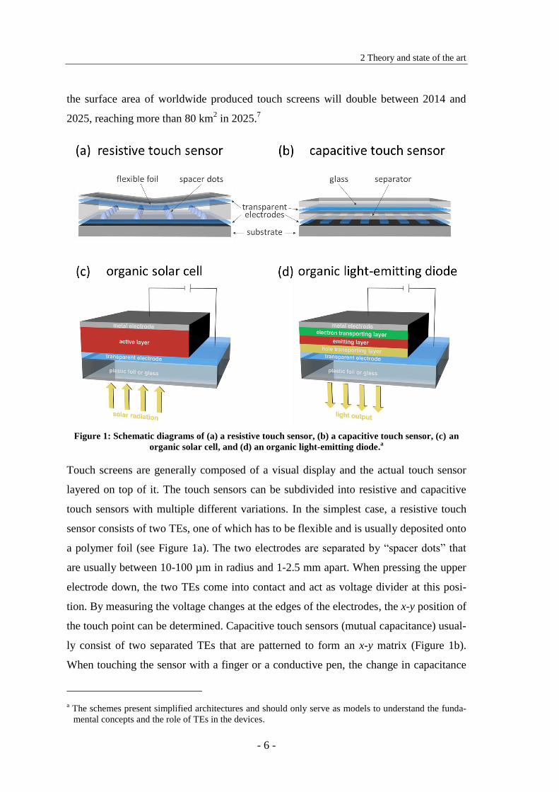
will be discussed and the respective requirements deduced. Figure 1 shows schematic
diagrams of the basic device architectures of resistive and capacitive touch sensors,
organic solar cells (OSCs), and organic light emitting diodes (OLEDs).
The field of touch sensors is a rapidly growing market for TEs. The applications range
from consumer electronics including mobile phones, notebooks, and tablets to house-
hold electronics like coffee makers, microwaves, or home entertainment systems that
more and more get equipped with touch-sensitive screens. Market forecasts predict that
a Many terms have been used to describe materials with concomitant optical transparency and electrical
conductivity, including “Transparent Conductive Materials (TCMs)”, “Transparent Electrodes (TEs)”,
“Transparent Conducting Films (TCFs)”, “Transparent Conductive Electrodes (TCEs)”, and “Transpar-
ent Conducting Coatings (TCCs)”, amongst many others. Each term emphasizes slightly different as-
pects. In this thesis, the term “Transparent Electrodes (TEs)” will be solely used as it appears to be the
most common.
2 Theory and state of the art
- 6 -
the surface area of worldwide produced touch screens will double between 2014 and
2025, reaching more than 80 km2 in 2025.
7
Figure 1: Schematic diagrams of (a) a resistive touch sensor, (b) a capacitive touch sensor, (c) an
organic solar cell, and (d) an organic light-emitting diode.a
Touch screens are generally composed of a visual display and the actual touch sensor
layered on top of it. The touch sensors can be subdivided into resistive and capacitive
touch sensors with multiple different variations. In the simplest case, a resistive touch
sensor consists of two TEs, one of which has to be flexible and is usually deposited onto
a polymer foil (see Figure 1a). The two electrodes are separated by “spacer dots” that
are usually between 10-100 µm in radius and 1-2.5 mm apart. When pressing the upper
electrode down, the two TEs come into contact and act as voltage divider at this posi-
tion. By measuring the voltage changes at the edges of the electrodes, the x-y position of
the touch point can be determined. Capacitive touch sensors (mutual capacitance) usual-
ly consist of two separated TEs that are patterned to form an x-y matrix (Figure 1b).
When touching the sensor with a finger or a conductive pen, the change in capacitance
a The schemes present simplified architectures and should only serve as models to understand the funda-
mental concepts and the role of TEs in the devices.
2 Theory and state of the art
- 7 -
at each electrode is measured and the exact touch position can be determined. Future
trends include large-area and flexible touch screens, as well as high resolution screens.8
Though still limited in efficiency and lifetime, organic solar cells (OSCs) have gained
interest due to their potential to be fabricated on flexible substrates and large-areas by
cost-effective roll-to-roll solution-phase processing.9 The basic architecture of organic
solar cells (Figure 1c) consists of two electrodes that enclose an active layer in which
light energy is converted into electricity by the photovoltaic effect. The active layer may
be a single layer, bilayer, or a bulk heterojunction, amongst others.10
The electrode fac-
ing the sun light should have minimum photon absorption to increase the efficiency of
the cell. The second electrode can be intransparent and is usually made from metals like
Al, Mg, or Cu. For solar cells, correct adjustment of the work functions of the different
layers is indispensable for an efficient operation.11
Future visions include fully transpar-
ent, flexible solar cells that are fabricated by wet methods and can be coated on win-
dows and curved polymer substrates.
Organic light emitting diodes (OLEDs) outperform conventional liquid crystal dis-
plays (LCDs) regarding brightness, efficiency, contrast, and, important for novel de-
signs, mechanical flexibility.12
The general architecture of OLEDs is akin to solar cells:
an active layer is sandwiched between two electrodes, one of which has to be transpar-
ent (Figure 1d). While in solar cells electron-hole pairs are created in the active layer,
OLEDs rely on their recombination to create photon emission. The active layer is often
a multilayer system composed of a hole transporting layer, an emitting layer, and an
electron transporting layer. Photon emission out of the device requires a transparent
electrode.13
Future trends comprise all solution-processed large-area lighting (wallpaper
displays or curtains), as well as rollable and portable displays.
2 Theory and state of the art
- 8 -
Requirements for transparent electrodes
Transparent electrodes are primarily evaluated by two major properties: optical trans-
mittance T (%)a and electrical sheet resistance Rs (Ω/sq)
b. The requirements for both
properties strongly depend on the specific application.14
A rough classification has been
reported by Hu et al.:15
– The optical transmittance should generally be ≥ 90% in the visible range for all de-
vices. For comparison, values are usually given for a specific wavelength (mostly at
500 or 550 nm). High optical transmittance is needed to ensure bright display images
in touch screens, increased power conversion efficiency in solar cells and high exter-
nal quantum efficiency in OLEDs.
– The required sheet resistances (Rs) vary by several orders of magnitude: For touch
screen applications, a sheet resistance in the range of 400–1000 Ω/sq is sufficient for
operation. A highly uniform electrical response of the TE must be guaranteed for ac-
curate touch sensing. OLEDs and solar cells require lower sheet resistance
(Rs ≤ 10 Ω/sq). High resistance would cause resistive heating and a non-uniform
emission in OLEDs; solar cells would suffer from decreased efficiency as their per-
formance relies on effective carrier collection before recombination and low cell se-
ries resistance.16–18
Several criteria (figures of merit) have been proposed to compare the performance of
TEs from different materials systems and processes regarding transparency and conduc-
tivity.19
Most used today is a metric based on the theory of Glover and Tinkham that
describes the transmittance T as a function of the sheet resistance Rs by
2
0
21
dc
op
sR
ZT
a The total optical transmittance Ttot is defined as the ratio Ttot = IT/I0 of the intensity of light transmitted
through a material (IT) to the intensity of the incident light (I0) and is usually given in %
(%T = IT/I0 x 100). The total transmittance Ttot can be subdivided into the ballistic transmittance Tbal that
accounts for the light transmitted parallel to the incoming beam and the diffuse transmittance Tdif that
accounts for the diffuse transmitted light (Ttot = Tbal + Tdif). For TEs, the ballistic optical transmittance is
the most relevant parameter. It is usually simply given as “(optical) transmittance T” in literature, which
has been adopted for this thesis, unless stated explicitly otherwise. b The sheet resistance has been introduced as a measure of resistance for thin films with homogeneous
thickness and is defined as
with the resistivity and the film thickness t. See section 8.2 for fur-
ther information.
2 Theory and state of the art
- 9 -
with Z0 (= 377 Ω) being the vacuum impedance and σdc and σop the optical and dc con-
ductivities of the material.20–22
The transmittance T is measured in the visible wave-
length range and mostly given at λ = 550 nm. The ratio σdc/σop serves as figure of merit.
The theory of Glover has been extended and refined for specific systems in recent stud-
ies.19,23
Other important properties include:
– The “haze”, which quantifies the fraction of transmitted light scattered at wide an-
gles and is usually defined as the ratio between diffuse and total transmittance.a The
required haze value strongly depends on the application: Touch screens, for example,
require low haze (< 3%) to avoid blurred viewing of the display.13,24
On the contrary,
electrodes with high haze may enhance the performance of solar cells: greater scat-
tering of the incoming photons increases their optical path length and thus the proba-
bility of absorption, which is important especially for thin film solar cells.25–27
– The mechanical flexibility, which has recently become important and is challenging
the state-of-the art materials (see section 2.1.4). The trend for novel flexible devices
on polymer substrates requires electrodes with high electrical stability upon bending
and folding to turn visions like rollable displays or wearable solar cells into reality.
While electrical resistance and optical transmittance are well defined parameters and
standardized test methods are available, there is no standard for measuring the bend-
ing stability of TEs (yet). Most commonly used in scientific publications is the rela-
tive change in resistance (R−R0)/R0 as a function of bending cycles. The bending ra-
dius is usually chosen between 1–20 mm. Many publications also report the change
in resistance as a function of the bending radius. The specific requirements again
strongly depend on the application.
– The surface roughness: In particular for multilayer thin film devices like OLEDs
and OSCs, the surface roughness must be below the thickness of a typical active lay-
er (often ~ 50-100 nm) to avoid short circuiting of the device.28,29
– The work function of the layers (important for OLEDs and solar cells).2
– The adhesion of the film to the substrate.30
– The electrical long-term stability with humidity and temperature.14
a According to ASTM D1003, the haze of a material is defined as the fraction of light that is scattered at
angles greater than 2.5° in forward direction.
2 Theory and state of the art
- 10 -
2.1.2 Transparency-conductivity trade-off
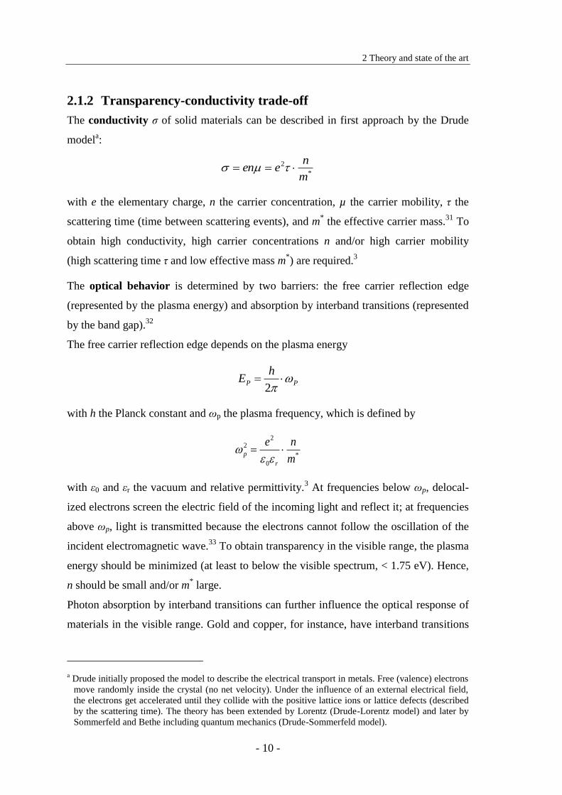
The conductivity σ of solid materials can be described in first approach by the Drude
modela:
*
2
m
neen
with e the elementary charge, n the carrier concentration, µ the carrier mobility, τ the
scattering time (time between scattering events), and m* the effective carrier mass.
31 To
obtain high conductivity, high carrier concentrations n and/or high carrier mobility
(high scattering time τ and low effective mass m*) are required.
3
The optical behavior is determined by two barriers: the free carrier reflection edge
(represented by the plasma energy) and absorption by interband transitions (represented
by the band gap).32
The free carrier reflection edge depends on the plasma energy
PP
hE
2
with h the Planck constant and ωp the plasma frequency, which is defined by
*
0
22
m
ne
r
p
with ε0 and εr the vacuum and relative permittivity.3 At frequencies below ωp, delocal-
ized electrons screen the electric field of the incoming light and reflect it; at frequencies
above ωp, light is transmitted because the electrons cannot follow the oscillation of the
incident electromagnetic wave.33
To obtain transparency in the visible range, the plasma
energy should be minimized (at least to below the visible spectrum, < 1.75 eV). Hence,
n should be small and/or m* large.
Photon absorption by interband transitions can further influence the optical response of
materials in the visible range. Gold and copper, for instance, have interband transitions
a Drude initially proposed the model to describe the electrical transport in metals. Free (valence) electrons
move randomly inside the crystal (no net velocity). Under the influence of an external electrical field,
the electrons get accelerated until they collide with the positive lattice ions or lattice defects (described
by the scattering time). The theory has been extended by Lorentz (Drude-Lorentz model) and later by
Sommerfeld and Bethe including quantum mechanics (Drude-Sommerfeld model).
2 Theory and state of the art
- 11 -
with energies in the visible spectrum that cause the characteristic coloring. In semicon-
ductors with high energy band gaps (> 3 eV) interband transitions occur above the visi-
ble spectrum.34
In summary, the ratio of the carrier concentration and the carrier effective mass (n/m*) is
the key factor for the design of transparent conductors, which simultaneously reveals
the trade-off between conductivity (n/m* should be maximized) and transparency (n/m
*
should be minimized)a: high carrier concentrations and low effective carrier mass re-
quired for high conductivity will shift the free carrier reflection edge into the visible
range and thus cause reflectivity of the material.32
Metals, the best electrical conductors,
have high carrier concentrations (n >> 1022
cm-3
) and thus a plasma edge in the deep-
UV spectral range.b A successful strategy for TE design is to use materials with limited
carrier concentrations, but increase the mobility of the charge carriers (see next sec-
tion).3
2.1.3 Transparent conductive oxides
Transparent conductive oxides (TCOs) were the first TE-materials applied in optoelec-
tronic devices and are still major players in the field of TEs.3 Their unique balance of
transparency and conductivity follows from wide-bandgap n-type semiconductors with
low electron effective mass (In2O3, ZnO, SnO2) doped to increase carrier concentra-
tion.3,34
The high energy band gap ensures that absorption by interband transitions is
shifted above the visible spectrum (> 3 eV). The intrinsically low carrier concentration
can be increased by doping, limited by the dopant’s solubility in the host material.c As
the attainable carrier concentrations are still relatively low compared to metals (about a
factor of 50-100), the plasma energy is still far below the visible spectrum and light is
transmitted in this wavelength range.3 The limited carrier concentration requires high
mobility of the charge carriers to obtain high conductivity. The mobility μ = eτ/m* is
a Precisely only holds for homogeneous materials.
b Recently, Zhang et al. reported transparent conductors based on correlated metals, which combine high
carrier concentrations with low plasma energies because strong electron-electron interactions result in a
high effective electron mass.32
c Doping of the host material also influences the width of the band gap.
202,203 Two mechanisms compete:
(1) band gap widening by the Burstein-Moss effect: doping leads to population of states within the con-
duction band, which increases the Fermi level. (2) band gap narrowing by many-body effects: electron-
electron scattering and electron-impurity scattering causes valence and conduction band to shift. For
doped In2O3, the interplay of both mechanisms result in a net increase of the gap.203
2 Theory and state of the art
- 12 -
determined by the scattering time τ (should be maximized) and effective carrier mass m*
(should be minimized). The scattering time is intrinsically limited by scattering at ion-
ized impurities caused by the dopant. Additional scattering at crystallographic defects
(dislocations, grain boundaries, etc.) can be reduced by appropriate deposition and an-
nealing. Thus, high-temperature post-processing steps are often necessary for TCOs
with high-end performance.34,35
The second important parameter is the effective mass,
which should be reduced to increase mobilitya. In particular, oxides of the post-
transition metal cations (“TCO cations”) Zn2+
, Cd2+
, In3+
, Sn4+
show small electron ef-
fective masses as their overlapping s-orbitals form broadly dispersed conduction
bands.3,36,37
ZnO:Al+, SnO2:F
+/Sb
+, and In2O3:Sn (ITO) are the most prominent materi-
als owing to their large bandgap (> 3 eV) enabling the use in the visible and near-
infrared (NIR) range.3 Among all, ITO shows the best performance and has been almost
exclusively used in optoelectronic devices; mobilities up to 100 cm2V
-1s
-1 result in resis-
tivities down to 1-2∙10-4
Ω∙cm.3 Sputtered ITO coatings (on glass) usually have a trans-
mittance about 90% at a sheet resistance ≥ 10 Ω/sq, which serves as benchmark for new
technologies (see next section).5,35,38
2.1.4 Solution-based transparent electrodes for flexible devices
Though still more than 90% of the entire TE market is dominated by ITO, several limi-
tations and undesirable properties have led to a copious research interest to replace ITO
in the last decade.2,39
Commonly stated motivations include the scarcity of indium and
the accompanying high raw material price; the concentration of production to few coun-
tries (China, Japan, Canada, etc.) and the concomitant strategic dependence further mo-
tivated the search for alternatives (particularly in Europe and the United States). Limited
resources of indium certainly conflict with the strongly increasing demand for optoelec-
tronic devices, but it should be noted that the cost of raw indium constitutes only 2% of
the total costs for ITO production. The major cost drivers are the slow and inefficientb
sputter process in vacuum and subsequent high-temperature post-processing steps re-
quired for high-grade ITO (see section 2.1.3).34,35
a As n is still rather low, a decrease in m* (thus, an increase in n/m
*) can be tolerated without shifting the
plasma energy in the visible range.36
b Large fractions of the sputtered target end up at the walls of the chamber.
5
2 Theory and state of the art
- 13 -
Nevertheless, cost arguments (raw material prices, process costs) are always subject to
fluctuations and should not be considered a single exclusion criterion. Raw indium pric-
es have significantly fallen in the last 2 years and leading ITO suppliers have recently
slashed their prices, which is impeding the replacement of ITO in established devices
and processes.40,41
Novel flexible devices based on polymer substrates entail new requirements that signifi-
cantly impede (if not exclude) the use of ITO: (1) ITO shows only limited bendability
due to its ceramic brittleness. Cracks form already at low strains and lead to a sharp
increase in resistance. (2) High-grade ITO requires processing at elevated temperatures
exceeding the thermal budget of many polymer foils.3,5,34,35
Hence, new materials with optoelectronics properties comparable to ITO (T ≥ 90%,
Rs ≤ 10 Ω/sq) that can be processed at low temperatures and are flexible enough to
withstand repeated bending cycles at low bending radii have been the focus of intense
research in the last decade. The search for ITO replacement materials has been accom-
panied by the wish to replace vacuum technology as a major cost driver by solution-
phase processing. Solution-phase processing has the potential to coat large areas (sever-
al meters wide) at high speeds (up to 100 m/min), while having lower capital and
maintenance costs than vacuum processing.5,42
The following sections will solely focus
on alternatives that can be coated from solution.
Conductive polymers were among the first alternatives in the late 20th
century.2 Poly-
mers can be coated from solution and are mostly flexible. The prevalent polymers are
polythiophene derivatives like PEDOT:PSSa, which is often used as hole injection layer
for OLEDs.43,44
High optical transmittance (T > 90%) can be obtained, but relatively
high sheet resistances (Rs > 100 Ω/sq) and limited stability under exposure to high tem-
perature, humidity, and UV radiation impede the use of conductive polymers in certain
applications.5,45,46
The second major class comprises carbon materials, including carbon nanotubes
(CNTs) and graphene. CNTs have been considered a promising alternative since their
discovery in the 1990’s because of their outstanding electrical properties: individual
a poly(3,4-ethylenedioxythiophene) poly(styrenesulfonate)
2 Theory and state of the art
- 14 -
CNTs have high carrier mobilities exceeding 100 000 cm2/Vs and can reach conductivi-
ties up to 200 000 S/cm.2 Transparent films were fabricated from CNT inks by solution-
based deposition processes including spray coating47
, Meyer rod coating48
, and dip coat-
ing.49
The expectations on CNT-based TEs were reduced by the difficulty to achieve
CNTs with high purity in large amounts and the limited conductivity of CNT thin films
due to large contact resistances between the individual CNTs.2
Considered the “rising star” in materials science, graphene is a promising candidate for
transparent electronics, too, based on its outstanding electrical (ultrahigh mobilities) and
optical (only 2.3% loss in transmittance per single layer) properties.50,51
However, TEs
from solution-processable inks based on graphene flakes underperformed the theoretical
expectations facing the same problem of large contact resistances as observed for CNT
inks.2 High-end TEs were reported only by chemical vapor deposition (CVD).
51–55
Metals, the best electrical conductors, are opaque in bulk: high carrier concentrations,
which enable the superior electron transport, imply high reflectivity in the visible range
(see section 2.1.2). Metal films can become optically transparent when they are thin
(usually less than 10 nm), but discontinuous growth impedes the fabrication of such
layers and electron surface scattering will limit the electrical conductivity at this thick-
ness.2,56
A second strategy can overcome these limitations: use thin metal
(nano)structures that carry the electrical current but are sufficiently small to avoid
strong light scattering in the visible range and separate them by voids that account for
the transmission of light. The transparency/conductivity ratio depends on the area frac-
tion that is covered by the material. First approaches included metal microgrids based
on “top-down” vacuum processing. Today, “bottom-up” approaches where metal
nanostructures are deposited from liquid dispersions reduce the required amount of ma-
terial and simplify the deposition process.4 Two main classes can be distinguished: ran-
dom nanowire networks (section 2.1.4.1) and ordered metal grids (section 2.1.4.2).
2.1.4.1 Random metal nanowire networks
Solution-phase synthesized metal nanowires with diameters between 20-150 nm and
lengths of 50-200 µm are dispensed onto a substrate in a random arrangement. At cer-
tain area fraction, the interconnected wires percolate and form a continuous electrical
2 Theory and state of the art
- 15 -
pathway. For applications as TEs, nanowire densities above the percolation threshold
are required.5
The optoelectronic properties of the layers are primarily set by the area fraction
DLNAF
with N the number of nanowires per unit area, the wire length L, and the diameter D.5
The transmittance of random networks can be estimated by
DL
CAF ext
eT
with the extinction cross-section Cext that is the amount of light absorbed and scattered
by a single nanowire.5
The resistance for N above percolation can be estimated in first approximation by
AmR NW
s/
where ρ∞ (Ω∙m) is the bulk resistivity of the material, ρNW (kg∙m-3
) is the nanowire den-
sity in the film, and m/A (kg∙m−2
) is the mass of the nanowires per unit area.5 The equa-
tion, however, disregards two fundamental characteristics of nanowire networks:
(1) The resistivity of a nanowire is always higher than the bulk resistivity due to elec-
tron surface scattering.56
(2) Contact resistances between the individual wires play a
major role and determine the overall sheet resistance of the film.57,58
After synthesis,
nanowires are typically surrounded by a polymeric ligand shell (e.g. polyvinylpyrroli-
done (PVP)) that stabilizes the wires in solution, but provokes high resistances at the
wire-wire junction.57
Two complimentary approaches can be applied to improve the
overall conductivity of a metal nanowire network: reduce number of interfaces or re-
duce electron barrier at the interfaces. At a fixed area fraction, increasing wire length
will reduce the number of interfaces for a given distance, which motivates the use of
ultrahigh aspect ratio wires.58
In contrast to carbon materials (see section 2.1.4), metal
nanostructures can be welded together by a sintering treatment. Removal of ligands and
subsequent formation of direct metal-metal contact significantly reduces the contact
resistances (see also section 2.3).
2 Theory and state of the art
- 16 -
The best-studied wire-based TEs are silver nanowires (AgNWs). During the last 5-10
years, a large number of articles has been published on AgNW networks and even vast
amounts of reviews exista.5,13,38
Various wet-coating methods have successfully been
applied to fabricate TEs based on AgNW networks, including drop casting,59
spray-
coating,60
rod-coating,61
spin-coating,62
and vacuum filtration with subsequent
transfer.63,64
Large-area TEs with optoelectronic properties comparable to ITO
(T > 90%, Rs < 10 Ω/sq) but with superior mechanical flexibility were reported in litera-
ture. Several companies were founded (many as university spin-offs) focusing on syn-
thesis and/or application of AgNWs including BlueNano, Seashell technologies, Cam-
brios, C3Nano, among others.
Second major player are copper nanowires (CuNWs).65–67
Copper is 6% less conduc-
tive than silver, but 1000 times more abundant and significantly cheaper. TEs of
CuNWs with comparable properties to AgNW networks and ITO have been reported in
literature, but copper’s high susceptibility to oxidize limits the long-time stability of
CuNW films. Novel approaches are trying to circumvent this drawback by overgrowing
the copper core with oxidation-resistant metals, for instance.65,68
Although random nanowire networks are close to application, there is still no commer-
cial breakthrough.69
Apart from business arguments, several technological issues may
cause the sluggish replacement of ITO:
- Random deposition allows only for limited control of the network geometry. The
nanowire density can be tuned, but not the position of individual wires.
- Haze values of several % impedes the use in high-end touch screens.13,70
- High surface roughness of the lose nanowire networks challenges the fabrication of
multilayer thin-film devices like OLEDs.29
Recent studies reported ultra-smooth
AgNW films by mechanical pressing or polymer coating.29,59,61
2.1.4.2 Ordered metal grids
Grids with controlled geometry have shown the potential to outperform ITO with regard
to electro-optical properties and mechanical flexibility.71
Several advantages over ran-
dom nanowire networks exist: Control over the grid’s microstructure enables the specif-
a Literature search on web of science (accessed Feb 20
th 2017) yielded 567 publications and 15407 cita-
tions for the combination “silver nanowire AND transparent electrode”.
2 Theory and state of the art
- 17 -
ic tuning of the properties for a particular application. Material is only placed where it is
needed; no isolated wires or dangling wire parts exist that reduce transmittance but do
not actively take part in the current transport.72
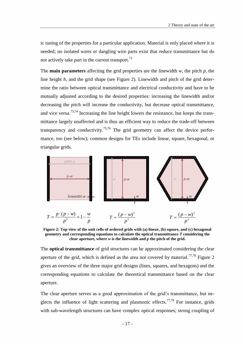
The main parameters affecting the grid properties are the linewidth w, the pitch p, the
line height h, and the grid shape (see Figure 2). Linewidth and pitch of the grid deter-
mine the ratio between optical transmittance and electrical conductivity and have to be
mutually adjusted according to the desired properties: increasing the linewidth and/or
decreasing the pitch will increase the conductivity, but decrease optical transmittance,
and vice versa.73,74
Increasing the line height lowers the resistance, but keeps the trans-
mittance largely unaffected and is thus an efficient way to reduce the trade-off between
transparency and conductivity.75,76
The grid geometry can affect the device perfor-
mance, too (see below); common designs for TEs include linear, square, hexagonal, or
triangular grids.
p
w
p
wppT
1
)(2
2
2)(
p
wpT
2
2)(
p
wpT
Figure 2: Top view of the unit cells of ordered grids with (a) linear, (b) square, and (c) hexagonal
geometry and corresponding equations to calculate the optical transmittance T considering the
clear aperture, where w is the linewidth and p the pitch of the grid.
The optical transmittance of grid structures can be approximated considering the clear
aperture of the grid, which is defined as the area not covered by material.77,78
Figure 2
gives an overview of the three major grid designs (lines, squares, and hexagons) and the
corresponding equations to calculate the theoretical transmittance based on the clear
aperture.
The clear aperture serves as a good approximation of the grid’s transmittance, but ne-
glects the influence of light scattering and plasmonic effects.77,79
For instance, grids
with sub-wavelength structures can have complex optical responses; strong coupling of
2 Theory and state of the art
- 18 -
surface plasmons in nanohole meshes has been reported to induce extraordinary trans-
mission, for example.80,81
The sheet resistance of a metal grid can be estimated using Kirchhoff’s law.77
For a
square nanowire network, the sheet resistance is
hw
L
N
NR
N
NR wires
11
with the resistivity ρ, the wire length L (equals the network pitch p), the linewidth w,
and the line height h. For large networks, the first term is close to unity, which leads to
(with L = p):
hw
pRs
The ratio between transparency and resistance is not the only factor affecting device
performance. For instance, Neyts et al. studied the voltage loss in metallic grids used for
OLEDs with different shapes (triangular, square, or hexagonal).73
Grids with identical
conductivity and transmittance were shown to have different voltage losses for different
geometries: a hexagonal mesh had 6% lower loss than a square grid. Solar cell perfor-
mance has been reported to depend on the geometry of grid-based TEs, too.82,83
The
influence of grid geometry on device performance underlines the superiority of grids
with controlled and tunable geometry over random meshes.
The fabrication of ordered metal grids started with established “top-down” processes:
lithographically prepared grids served as mask for subsequent metal evaporation. The
number of processing steps, waste of excess material, and complex vacuum technology
limit the cost-efficiency of this technology. In recent years, “bottom-up” processes that
additively deposit material from liquid dispersions have been shown to increase struc-
tural flexibility, reduce complexity, require fewer processing steps, and reduce the
waste of material (see next section).4
2 Theory and state of the art
- 19 -
2.2 Patterning of nanoparticle inks for electronics
A variety of technologies has been used to print defined structures from liquid inks con-
taining nanomaterials.39
Metal nanoparticle inks are usually dispersions of nanoparticles
with diameters below 100 nm and a metal content between 10 and 70%.84
The liquid
phase is usually a mixture of multiple solvents to adjust wetting, evaporation, etc.30,66
In the following section, the most relevant techniques for the fabrication of ordered
transparent metal grids will be discussed. Section 2.2.2 will introduce the novel concept
of direct nanoimprinting for high-resolution patterning of nanoparticle inks.
2.2.1 Fabrication of transparent metal grids from nanoparticle inks
Ahn et al. introduced the concept of direct writing of nanoparticle inks.85
A concentrat-
ed silver nanoparticle ink (mean particle size: 20±5 nm; solid content: 78 wt%) was
extruded through a tapered cylindrical nozzle that was translated using a three-axis ro-
botic motion stage. Square silver grids with a linewidth of 9 µm and height of 3 µm
were prepared with a varying pitch from 100-400 µm. Thermal annealing at 200°C for
2 h after printing yielded grids with resistivities down to 3.64∙10-5
Ω∙cm. Grids with a
pitch of 400 µm showed a transmittance of 94.1%.
Electrohydrodynamic (EHD) jet printing increases the resolution of inkjet
printing.86,87
Droplets much smaller than the actual nozzle diameter can be ejected by
applying a high electric field that stretches out the meniscus on the tip of the nozzle.
Jang et al. used a commercial silver ink (ENJET; solid content: 70 wt%) to print grids
with a linewidth of 7.53 µm, a height of 1.46 µm and a pitch between 50-300 µm from a
nozzle with an inner diameter of 100 µm. Grids with 150 µm pitch had an optical
transmittance of 81.75% and a sheet resistance of 4.87 Ω/sq after annealing at 200°C
under near-infrared light.86
Schneider et al. increased the resolution of the method in a
process called NanoDrip printing (droplet diameter: < 100 nm; nozzle diameter:
1 µm).88
They printed silver and gold nanogrids from commercial nanoparticle inks with
linewidths from 80 to 500 nm, heights between 200 nm and 1.5 µm, and pitches of
10-20 µm. The grids exhibited superior optoelectrical properties (Rs = 8-20 Ω/sq,
T = 94-97%) after thermal annealing at 150-250°C at low printing speeds of ~ 30 min
for the patterning of 100 µm2.
2 Theory and state of the art
- 20 -
The fabrication of grids by laser sintering was introduced by Hong et al.89
and Lee et
al.90
. Both fabricated transparent metallic grids on flexible substrates using selective
laser sintering of metal nanoparticle inks. Nanoparticles in suspension were first spin-
coated onto a substrate. A focused laser acted as local heat source sintering the particles
selectively to conductive microlines. Patterning and sintering were performed in a sin-
gle step (see also section 2.3.1). The applied laser power determined the temperature
distribution and thus, the structure of the sintered lines. Unsintered particles were re-
moved by a subsequent washing step. The resulting grids showed high transmittance
(> 85%) and low sheet resistance (30 Ω/sq). Laser sintering, as maskless direct writing
methods, allows for the fabrication of arbitrary structures and flexibility of the process.
Drawbacks of the method are limited resolution (linewidth 10-30 µm) and waste of the
unsintered parts of the ink layer.
Layani et al. introduced a printing process based on the combination of inkjet printing
and the coffee ring effect.91
Particles inside sessile suspension droplets are known to
assemble at the perimeter of the contact line upon evaporation if it is pinned, well-
known as coffee ring effect.92
Layani et al. ink-jetted drops of a silver nanoparticle ink
(mean particle diameter: 20 nm; solid content; 0.5 wt%) in a 2D-array. The particles
assembled into dense interconnecting metallic rings that had a linewidth of 10 µm, a
height < 300 nm, and a “hole” of 150 µm in average.91
The process yielded TEs with a
transmittance of 95% and a sheet resistance of 4 Ω/sq after annealing in HCl vapor (see
also section 2.3.2). The concept was extended by Zhang et al. who ink-jetted linear liq-
uid patterns (arrays of drops) of a silver nanoparticle ink.93,94
Upon evaporation, the
silver nanoparticles aggregated at the three-phase contact line and formed two parallel
lines. The distance between two parallel lines was 60–80 µm and the distance between
each set of double lines was set to 800-900 µm. They achieved square grids with a lin-
ewidth of 5-6 µm and a height of 0.3-0.4 µm on hydrophilic glass substrates. The result-
ing grid had a transmittance of 93.6% and a sheet resistance of 30 Ω/sq.
Higashitani et al. described a process named “evaporative lithography” yielding or-
dered metal grids based on AuNPs by templated evaporation.95
A gold nanoparticle dis-
persion (mean particle diameter: 10 nm; solid content: 2 wt%) was dropped on a stain-
less steel mesh that had been placed on top of a plasma-treated glass substrate. The so-
lution spread over both, mesh and glass substrate. During evaporation, the liquid flowed
2 Theory and state of the art
- 21 -
towards the bars of the steel mesh, forming a grid with open spaces. After drying, the
steel mesh was removed to obtain gold grids with a linewidth of 4 µm, a height of
80 nm, and a pitch of 100 µm. Sintering at 425°C for 20 min was necessary to remove
the organic ligands and to turn the grid conductive. The resulting grids showed transmit-
tance of 82% at a sheet resistance of 20 Ω/sq. Layani et al. extended the method to heat-
sensitive substrates using metallic nanoparticle inks that can be sintered at room-
temperature.96
Silver nanoparticles with polyacrylic acid as electro-steric stabilizer co-
agulated when exposed to HCl vapors (see section 2.3.2).97
The grids had an average
linewidth of 5.7 µm, a height of 1.1 µm, and a pitch of 50 µm. The optical transmittance
was 77% at a sheet resistance of 9 Ω/sq.
The concept of flow coating is based on the convective assembly of nanoparticles into
dense lines: a droplet of the nanoparticle dispersion is confined between an angled plate
and the substrate by capillary forces and forms a meniscus. Analogue to the coffee ring
effect described above, solvent evaporation at the three-phase contact line induces a
convective flux of solvent from the droplet that carries the nanoparticles to the contact
line, where they get deposited on the substrate.98
Linear movement of the plate stretches
the meniscus until the contact line slips to a new position. Repeated movement of the
plate after certain waiting times creates dense lines with defined spacing.99
Park et al.
reported the fabrication of transparent metallic grids by flow-coating of silver nanopar-
ticles.100
They prepared square grids with a linewidth of 7-10 µm, a height of 60 nm,
and a pitch of 200 µm. The grids had optical transmittances between 70-88% at sheet
resistances in the range of 132-332 Ω/sq. Flow coating is a simple method and does not
require a complex printing setup, but is limited regarding grid geometry. On unpat-
terned surfaces, only straight lines (parallel to the meniscus) can be prepared; intercon-
necting grids (like the square grids reported by Park et al.) require two step processing.
In nanosphere lithography, monolayers of polystyrene (PS) spheres serve as mask for
the fabrication of honeycomb meshes by deposition of material in the gaps between the
spheres, first with material deposition based on evaporation.101,102
Kwon et al. were the
first to report a fully solution-based process.103,104
They prepared silver meshes by coat-
ing a monolayer of PS spheres with a commercial silver ink (TEC-IJ-010, Inktec; solid
content: 11.5 wt%) using a Meyer rod. After curing the ink (5 min at 100°C then 10 min
at 140°C), the PS spheres were removed by sonication yielding conductive honeycomb
2 Theory and state of the art
- 22 -
meshes with linewidths between 0.03-0.5 µm, a height of 70-200 nm, and a pitch that
was dependent on the sphere diameter (600 nm, 3 µm, and 10 µm). Parasitic islands that
degraded the transmittance near the mesh lines were eliminated by wet etching. The
meshes had transmittances between 35-88% and sheet resistances ranging from 20 to
2000 Ω/sq.
Limitations
The described methods suffer from two common drawbacks: limited resolution and the
need for sintering at elevated temperatures.
Metal lines with several micrometer width do not guarantee the invisibility of the grid,
which limits the applicability as front electrode of displays, for example. The limited
resolution requires large separation of the lines (large pitch) to achieve high optical
transmittance. TEs with such large non-conductive holes do not perform well with de-
vices like OSCs or OLEDs.5,73,105
Surface roughnesses in the micrometer range make
thick metal grids incompatible with multilayer thin-film devices like OSCs or OLEDs.
The need for smaller linewidths has been pointed out by IDTechExa as a major issue:
“The battle between metal mesh suppliers will be fought on narrowing the linewidth and
improving throughput and yield (biggest cost unknown/driver).”106
In many cases, high temperature sintering is necessary to obtain low resistivity, which
exceeds the thermal budget of many polymer substrates and thus impedes the use of
such metal grids in the fabrication of modern flexible devices. Section 2.3 will discuss
the effects of sintering treatments on nanoparticle inks and present novel sintering tech-
niques.
2.2.2 Direct nanoimprinting of nanoparticles
Nanoimprint lithography (NIL) has become a powerful alternative to photolithogra-
phy for patterning materials with high resolutions (down to nm) at high throughput and
low costs.107,108
While in photolithography photons induce the patterning (e.g. develop
photo resist), NIL relies on direct mechanical deformation that does not have diffraction
limitations. A pre-patterned template, usually referred to as “stamp” or “mold”, is
pressed into material and replicates the patterns of the stamp.109
Many different types of
a IDTechEx provides market research and business intelligence with a strong focus on novel technologies
including Printed Electronics, 3D printing, RFID, wearables, etc.
2 Theory and state of the art
- 23 -
nanoimprint lithography have been developed over the years, some with resolutions in
the nanometer range and a vast field of applications.110
Usually, a thin polymer film or
resist is patterned, which is either directly used as a material (e.g. as diffraction gratings
or microfluidic devices) or serves as a mask for further processing steps like wet etching
or metal evaporation, for instance. To ensure a complete filling of the mold and a high
fidelity of pattern replication, the viscosity and surface tension of the imprinted material
need to be considered.109
The mold materials are usually classified regarding their
Young’s modulus (E):111
- rigid molds (E > few GPa): silicon, SiO2, glass, silicon nitride, nickel
- soft molds (E < few MPa): PDMS, polyurethane
- rigiflex molds (few MPa < E < few GPa): fluoropolymers
In conventional NIL, the stamp is placed in full contact with the substrate to imprint the
pattern (batch process), which limits the application for large-area patterning: large con-
tact areas require very large forces for high-resolution patterning; high adhesion forces
impede the stamp release without pattern destruction. In addition, long processing times
(few min or longer per wafer) interfere with the demand of high-throughput for practical
applications. For high-resolution and high-throughput patterning, the group of L. Jay
Guo investigated the transfer of NIL to roll-to-roll (R2R) processing.112–114
They at-
tached the stamp (flexible or rigiflex) onto a cylindrical roller and incorporated it into a
R2R setup enabling the imprinting of foils. As the effective imprinting area (contact line
transverse to web moving direction) is small, less force is necessary for successful pat-
terning and reduced adhesion forces facilitate the stamp release. Today, first commer-
cial R2R-NIL systems are available.115
The use of elastomers has several advantages over rigid molds: elastomers can make
conformal contact with substrates and allow for an easy release from rigid masters, even
for complex structures. The beneficial properties provoked the development of several
unconventional printing methods based on soft molds, grouped under the term “soft
lithography”.116,117
Soft lithography generates patterns with feature sizes between
30 nm and 100 µm by pre-patterned elastomeric stamps. The most commonly used
stamp materials are polydimethylsiloxanes (e.g. Sylgard 184) that has a low interfacial
free energy (∼21.6·10-5
N/cm), good chemical stability, thermal stability, gas permea-
bility, and optical transparency down to 300 nm.116
Stamp fabrication comprises the
2 Theory and state of the art
- 24 -
molding of PDMS by drop-casting onto a master with relief structures (e.g. lithograph-
ically patterned silicon wafers or nickel shims), curing, and peeling off.118
Micromold-
ing in capillaries (MIMIC) has been used for the patterning of nanoparticle inks. In
MIMIC, a PDMS stamp is placed in contact with a planar substrate creating capillary
channels by the groves in the PDMS. A drop of the nanoparticle ink is placed at the
ends of these channels. Capillary forces induce liquid filling of the cavities. After drying
or curing of the material, the PDMS stamp can be removed. The method is applicable to
a broad material range (liquid resist, nanoparticle solution, etc.) and enables the fabrica-
tion of features in the sub-100 nm scale.119,120
Duan et al. reported the fabrication of thin
metal lines and grids (feature size down to 40 nm) by molding of gold nanoparticles
(mean diameter: 3.5 nm).121
The capillary filling, efficient and fast over short distances,
is significantly slowed down with increasing distance due to viscous drag of the liquid,
which impedes the fabrication of large-area TEs.122
Small cross-sectional areas, re-
quired for high resolution, will further reduce the filling rate.119
In 2007, Ko et al. pioneered a process to fabricate metal structures with high resolution
that combines elements of classical nanoimprinting and soft lithography using nanopar-
ticle inks.123
The process is based on direct nanoimprinting of a nanoparticle ink by a
pre-patterned PDMS stamp and the subsequent sintering of the nanoparticles to a bulk
material. Direct patterning eliminates the need for intermediate mask steps and requires
only moderate temperatures and contact forces. The process consisted of several steps:
AuNPs (mean particle size: 1-3 nm; ligand: hexane thiol) were dispersed in α-terpineol
and dispensed onto a silicon substrate. A pre-patterned PDMS stamp was pressed into
the solution under the pressure of 5 psi (~ 0.35 bar) at 80°C; nanoparticles filled the
cavities, replicating the structure of the stamp. After solvent evaporation, the stamp was
removed and the particles were sintered on a hot plate at 140°C. The temperature during
printing affected the viscosity of the NP solution and had to be balanced for optimal
printing results: increased temperature decreased the viscosity of the solvent; at the
same time, increased temperature accelerated solvent evaporation and thus increased
viscosity. Ko et al. successfully printed test structures (lines, dots, etc.) with high reso-
lutions (feature size down to 100 nm) and tested the applicability of printed nanowire
resistors in organic field effect transistors. Only small areas in the range of 30 µm were
structured.
2 Theory and state of the art
- 25 -
The work of Ko et al. was followed by many derived processes to fabricate plasmonic
metallic structures. Liang et al. reported the fabrication of plasmonic metallic
nanostructures in a similar process and studied the influence of printing temperature and
pressure.124
A temperature of 60°C was not sufficient to ensure complete filling of the
cavities due to high viscosity; at 80°C, deformation of the stamp features was observed,
which the authors attributed to accumulation of solvent vapor in the cavities. The ap-
plied pressure was adjusted between 3-6 bar: increasing the pressure decreased the
amount of residual layer; at 6 bar, deformation of the stamp features led to poor pattern
fidelity. Fafarman et al. prepared subwavelength arrays of nanopillars, nanowires, and
nanoholes by direct nanoimprinting of a AuNP dispersion in hexane (mean particle di-
ameter: 10 nm; particle concentration: 18 mg/mL).125
Direct nanoimprinting of electronic materials has been largely restricted to the fabrica-
tion of electrodes for field-effect transistors (FETs). Park et al. reported printing of gold
source-drain electrodes for OFETs on polyimide using the same protocol (AuNPs in
α-terpineol; mean particle size: 1-3 nm; solid content: 10 wt%).126
The average resistivi-
ty of the printed structures was 1.99∙10–7
Ω·m, which is about 8 times the resistivity of
bulk gold. Hu et al. extended the method to silver inks (AgNPs in α-terpineol; mean
particle size: 10 nm, solid content: up to 15%). They fabricated organic FETs on flexi-
ble substrates using nanoimprinted silver electrodes and semiconducting polymers.127
Yu et al. engineered the ligand shell of gold nanoparticles (mean particle diameter:
2.5 nm) to provide imprintability.128
The ligand consisted of a thiol-group bonding to
the gold surface, a stabilizing alkyl chain, and a tetra(ethylene glycol) segment with a
cyclohexylammonium end-group that suppressed crystallization. In this way, they were
able to print conductive patterns with feature sizes down to 40 nm without solvent or
polymer additives.
In summary, direct nanoimprinting of colloidal nanoparticle dispersions is a suitable
method to create metal structures with nm resolution at low processing temperatures
(≤ 80°C), compatible with flexible polymer substrates. The scalability of classical NIL
suggests the potential of direct nanoimprinting to be transferred to large-area R2R pro-
cesses, too. Successful application to large-scale electronics will greatly depend on the
ability to ensure electrical connectivity over macroscopic distances. High pattern fideli-
ty and percolation of the particles will be key aspects.
2 Theory and state of the art
- 26 -
2.3 Sintering of nanoparticle inks for electronics
Electronic structures based on nanoparticle inks suffer from an inherent dilemma: ligand
molecules on the particles’ surface usually impede the electron transport between the
particles and limit the conductivity of the printed features.129
Nanoparticles from wet-
chemical synthesis are usually capped by organic molecules (ligands) that tune the par-
ticle size and shape during synthesis and inhibit particle agglomeration in dispersion by
electrostatic, steric, or electrosteric stabilization.130
Conductive metal inks with high
particle loads usually rely on steric stabilization by surfactant- or polymer-like am-
phiphilic organic molecules that bind to the nanoparticle surface via carboxyl, carbonyl,
amine, or thiol moieties.30,84
After deposition and drying of the ink, the organic stabilizers remain in the layer and act
as dielectric tunneling barriers provoking high contact resistances at the particle-particle
interfaces. To enable continuous electron transport between the particles, the insulating
ligands have to be removed in a post-treatment. A common approach is to apply thermal
energy by conventional methods like hot air in a convection oven or IR irradiation to
decompose the organic material. Typical sintering temperatures are 150-350°C with
processing times of 10-60 min.30
Novel concepts of “sintering-free” inks with conductive ligand shells that render the
sintering step obsolete are currently under scientific discussion, but only few publica-
tions exist. As an example, a novel sintering-free hybrid-ink has been developed by
Reiser et al., co-authored by the author of this dissertation.131
Gold nanoparticles were
capped with conjugated, electrically conductive polymers (PTEBS, PEDOT:PSS) that
simultaneously provided colloidal stability and enabled electron transport from particle
to particle. Printed lines were conductive (resistivity down to 0.04 Ω/sq/mil) after depo-
sition without additional sintering.
Sintering of nanoparticle inks commonly occurs in two stages: (1) removal of ligands,
(2) coalescence of the nanoparticles.84
After ligand decomposition or detachment, un-
protected particles coalesce by surface melting and diffusion of metal atoms from one
NP to another (high surface mobility), driven by the reduction of the free surface ener-
gy.30
The fusion of particles occurs at temperatures far below the melting point of bulk
gold (1064°C), a phenomenon called “melting point depression”.132
Atoms at surfaces
2 Theory and state of the art
- 27 -
have fewer bonds and thus lower cohesive energy than atoms in bulk; less energy is
necessary to move them. Nanoscale objects have large surface-to-volume ratios, which
increase with decreasing particle size and lead to a size-dependent melting point.133–135
Consequently, the required sintering temperature of small NPs is often set by the ligand
removal rather than by the actual melting point of particles.
The high temperatures that are required to remove the stabilizers from NP inks (in the
range of 150-400°C) require substrates like glass or silicon, but exclude most polymer
substrates. Standard polymer foils have low thermal stability with glass transition tem-
peratures on the order of 150°C; extended sintering at temperatures above will lead to
severe foil deformation.84
Novel sintering technologies should minimize the thermal
impact on the substrate, but retain fast sintering for high throughput processing. Among
many other publications, I would like to highlight the review of Schubert et al., which
presents a good summary of novel concepts for sintering of NP inks.84
Three of the
most relevant technologies are based on photonic sintering (section 2.3.1), chemical
sintering (section 2.3.2), and plasma sintering (section 2.3.3).
2.3.1 Photonic sintering
The basic idea of “photonic sintering” is to selectively heat the ink by the photothermal
effect at wavelength where the ink has high absorption but the substrate has not. Metal
nanoparticles commonly show strong surface plasmon resonances in the visible range,
while substrate like glass and polymer absorb mostly in the UV range. Since the absorp-
tion characteristics change with the specification of the ink (base material, particle dis-
tribution, etc.), the process parameters (spectrum, power density) have to be adjusted for
each system. Several technologies based on “photonic sintering” have been developed:
Near-infrared (NIR) sintering
Most polymers do not have strong absorbance in the NIR range (700–1500 nm). Irradia-
tion in this wavelengths range will selectively sinter the ink and limit the energy input
on the substrate minimizing substrate deformations.136
NIR sintering is scalable and
suitable for high-throughput R2R processing, commercial systems are readily availa-
ble.137
As the timescale of sintering is in the order of seconds, heat transfer from metal
ink into substrate cannot be fully neglected, which makes NIR more suitable for sub-
strates like paper than for ultrathin PET foil.84
In the course of the process, the absorp-
2 Theory and state of the art
- 28 -
tion behavior of the ink constantly changes as particle size and shape change upon sin-
tering.84
Hence, the sintering characteristics change and kinetics are often slowed-down.
Intense pulsed light (IPL) sintering
Continuous irradiation with light will heat up the particles, but the need to attain thermal
equilibrium with the substrate will cause heat transfer to the substrate within millisec-
onds. Intense pulsed light with a pulse duration (tpulse) much shorter than the time to
achieve thermal equilibration between ink and substrate (τsubstrate) heats the particles (by
light absorption) locally before they can transfer the heat to the substrate.138
For a
homogeneous sintering, the pulse duration should be longer than the thermal equilibra-
tion time of the ink (τink). While τink is of the order of one microsecond or below, τsubstrate
is at least several tens of milliseconds, which opens a window for the pulse duration
(τink < tpulse < τsubstrate). The high energy density leads to locally high process tempera-
tures, which reduces the processing time and thus increases throughput. Most common-
ly used are xenon stroboscope lamps with irradiation at wavelengths between 200 and
1200 nm. Appropriate conditions (pulse length, pulse intensity, flashing frequency, etc.)
have to be chosen for each ink/substrate combination.84
IPL treatment has been successfully used for sintering of copper inks139,140
,
AgNWs141,142
, and silver inks.143,144
Several commercial systems are available from
Novacentrix (Pulse Forge series) and Heraeus noble light.145,146
Sintering by pulsed light is a cheap and energy efficient technique (30% of electrical
energy converted into radiation, no complex optics necessary as for laser).147
It is easily
scalable and can be integrated into R2R systems.148
For certain ink formulations, the
high surface temperatures reached can lead to oxidation of the ink material under air;
foil deformation has been observed after multiple flashing.149
Laser sintering
Nanoparticles absorb the photons emitted from a laser, heat up by the photothermal ef-
fect, and sinter together. Controllable parameters are power output, writing velocity,
wavelength, and operation mode (continuous wave or pulsed), which have to be chosen
carefully to minimize the heat dissipation into the substrate material.
Ko et al. reported on the selective laser sintering of inkjet-printed microlines from gold
nanoparticles.150
The ink was dried and then locally sintered by scanning with a focused
2 Theory and state of the art
- 29 -
Ar-ion laser (wavelength: 514.5 nm); unsintered nanoparticles were removed with or-
ganic solvents. Laser sintering can be used as a direct structuring method as well: metal-
lic grid transparent conductors have been prepared by laser sintering of spin-coated par-
ticle suspensions on flexible substrates (see also section 2.2).89,90
Laser sintering is versatile, arbitrary patterns can be sintered in a mask-less process.
Locally high temperatures can cause damage to the substrate and to the ink (ablation of
metal). Spot sizes of only a few mm leads to long processing times for large areas.
2.3.2 Chemical sintering
Chemical sintering involves the destabilization of the particle/ligand system by decom-
position or exchange of the organic ligand molecules in the presence of a sintering
agent.
One approach is the chemical decomposition of the ligands. Magdassi et al. showed
that AgNPs capped with negatively charged poly(acrylic acid) (PAA) spontaneously
coalesce when coming into contact with the oppositely charged polyelectrolytes
poly(diallyldimethylammonium chloride) (PDAC).97
The degree of coalescence can be
tuned by the ratio between silver and PDAC. The PDAC was added by inkjet printing
on top of the silver array. The process yielded highly conductive (5 times the resistivity
of bulk silver) traces at room temperature, though many voids were present between the
sintered zones. The Magdassi group further showed that PAA-stabilized AgNPs can
undergo self-sintering in the presence of Cl− ions as destabilizing agent.
151 Cl
− ions re-
place the carboxylate anchoring groups of the PAA, which subsequently detaches from
the nanoparticles' surface and enable particle coalescence at room temperature. NaCl
solution or HCl vapor were applied as Cl− source. Sintered lines had a resistivity of
3.84∙10-6
Ω∙cm (~2.5 times the resistivity of bulk silver).
Other approaches involve the exchange of long stabilizing ligands by short ligands after
layer deposition. Reduced inter-particle spacing eases the electron transport from parti-
cle to particle and enhances conductivity.a Fafarman et al. reported the exchange of
long-chain OAm ligands on AuNPs by the short inorganic ammonium thiocyanate
(NH4SCN).125,152
The resistance of spin-coated AuNP layers dropped by 10 orders of
a The tunneling rate increases exponentially with decreasing separation between the NPs.
129
2 Theory and state of the art
- 30 -
magnitude upon the ligand exchange. The layers were simply dipped into the thiocya-
nate solution (1 wt% NH4SCN in acetone) after deposition.
Chemical sintering is often done at room temperature and minimizes the thermal input
on ink and substrate, but compatibility of the substrates with the used solvents has to be
guaranteed. Chemical reactions are often limited to specific ligand systems, which re-
stricts the range of application. Post-treatment of printed layers in liquids can influence
the stability of the layers; Fafarman et al. had to pre-coat the substrates by a mercapto-
propyltrimethoxysilane (MPTS) layer to avoid particle desorption, for instance.125
2.3.3 Plasma sintering
Ionized gasses formed by applying large energy (thermal, electric current or electro-
magnetic irradiation, etc.) are referred to as plasmas.84
Plasma interacts with materials
in several ways: highly reactive species (radicals, low-energy ions, and electrons) in-
duce chemical reactions; the impingement of particles causes sputtering of the surface
by momentum transfer and some heating of the material.153
Together, they lead to the
decomposition of organic material, e.g. by chain scission. The resulting low molar mass
compounds are generally volatile and can be easily removed, especially at low pres-
sures. Hence, plasma treatment is used as a standard method to remove organic residues
from substrates.153
Plasmas can be oxidizing (oxygen, air), reducing (hydrogen), or inert
(noble gases, nitrogen). The ability to decompose organic material at low thermal budg-
et makes plasma sintering an interesting approach to decompose and remove organic
ligands.154
The resulting highly reactive free metal surfaces can coalesce as described
above without further temperature treatment.
Reinhold et al. treated inkjet-printed silver nanoparticle inks (roughly one micrometer
thick) on common polymer foils by low-pressure argon plasma. Under the influence of
the plasma, the silver particles coalesced into clusters as confirmed by XRD. The resis-
tivity of the printed line was less than one order of magnitude above that of bulk
silver.155
Pronounced coalescence of the particles (as in the case of Reinhold) will de-
stroy the nanoparticle size-dependent properties. Ozin and Cademartiri introduced a
novel concept named “nanocrystal plasma polymerization” (NPP).156
A soft, low-energy
plasma treatment only partially removed the ligand shell while preserving the size-
2 Theory and state of the art
- 31 -
dependent properties of the nanoparticles. An inorganic matrix connecting the particles
enables the fabrication of mechanically stable and free-standing 3D architectures.
Plasma sintering has several advantages and disadvantages over traditional thermal sin-
tering. Ligand decomposition does not require high temperatures, which limits the
thermal budget of the method and makes it compatible with fragile substrates. The pro-
cess is limited in depth by a phenomenon called “skin effect”: during plasma treatment
a sintered top crust is formed, which prevents the plasma from penetrating the material.
Depending on the choice of plasma, the treatment can be time-consuming (Reinhold
reports treatment times of up to 1 h).155
Long processing times will also affect the sub-
strate, which can be detrimental for multilayer systems.157
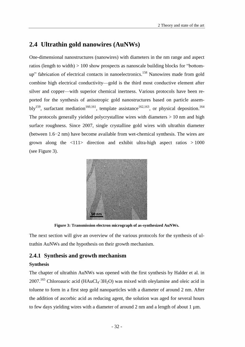
2 Theory and state of the art
- 32 -
2.4 Ultrathin gold nanowires (AuNWs)
One-dimensional nanostructures (nanowires) with diameters in the nm range and aspect
ratios (length to width) > 100 show prospects as nanoscale building blocks for “bottom-
up” fabrication of electrical contacts in nanoelectronics.158
Nanowires made from gold
combine high electrical conductivity—gold is the third most conductive element after
silver and copper—with superior chemical inertness. Various protocols have been re-
ported for the synthesis of anisotropic gold nanostructures based on particle assem-
bly159
, surfactant mediation160,161
, template assistance162,163
, or physical deposition.164
The protocols generally yielded polycrystalline wires with diameters > 10 nm and high
surface roughness. Since 2007, single crystalline gold wires with ultrathin diameter
(between 1.6−2 nm) have become available from wet-chemical synthesis. The wires are
grown along the <111> direction and exhibit ultra-high aspect ratios > 1000
(see Figure 3).
Figure 3: Transmission electron micrograph of as-synthesized AuNWs.
The next section will give an overview of the various protocols for the synthesis of ul-
trathin AuNWs and the hypothesis on their growth mechanism.
2.4.1 Synthesis and growth mechanism
Synthesis
The chapter of ultrathin AuNWs was opened with the first synthesis by Halder et al. in
2007.165
Chloroauric acid (HAuCl4·3H2O) was mixed with oleylamine and oleic acid in
toluene to form in a first step gold nanoparticles with a diameter of around 2 nm. After
the addition of ascorbic acid as reducing agent, the solution was aged for several hours
to few days yielding wires with a diameter of around 2 nm and a length of about 1 µm.
2 Theory and state of the art
- 33 -
In 2008, several papers on the synthesis ultrathin AuNWs were published in a very short
time framea by groups around the major players in the field of colloidal
nanomaterials.166–169
The synthetic protocols vary slightly, but follow the same concept:
OAm acts as reducing agent and structure-directing agent at the same time. Because
OAm is a liquid at room temperature it can be the solvent, too. The syntheses comprise
the dissolution of chloroauric acid in OAm in the right stoichiometry and subsequent
aging. As no additional reducing agent is used, the synthesis required long reaction
times (4-5 days) and elevated temperatures (35-80°C). Only Lu et al. added AgNPs as
reducing agent, but the reaction still required several days of ageing.169
The protocols
consistently yielded wires with diameters between 1.6-1.8 nm; only Wang et al. showed
diameters between 3-9 nm.166
The length of the wires was estimated to be in the range
of 1-4 µm, although no direct experimental proof has been reported.
Feng et al. accelerated the reduction process by adding triisopropylsilane (TIPS) as ad-
ditional reducing agent.170
In their protocol, 3 mg HAuCl4 were mixed with 100 mL
OAm and 2.5 ml n-hexane, followed by the addition of 150 mL TIPS. The solution was
kept undisturbed (no stirring) at room temperature for several hours until a gradual color
change from yellow to dark red was observed. The protocol yielded wires with 1.8 nm
in average diameter in a fast and robust synthesis and served as basis for many publica-
tions, including this thesis.
After synthesis, washing of the wires removes unreacted educts and excess oleylamine.
Although slightly different protocols have been reported, the fundamental concept stays
the same: addition of a polar solvent (usually ethanol or mixtures of ethanol and the
respective solvent of the synthesis) induces agglomeration of the wires into macroscopic
bundles, which precipitate (often assisted by centrifugation). After removal of the su-
pernatant, the precipitated wires can be redispersed in the desired solvent; alkanes (hex-
ane, octane, etc.), cycloalkanes (cyclohexane, cyclooctane, etc.), arenes (benzene, tolu-
ene), tetrahydrofurane (THF), and chloroform have been reported.
a submitted between 6
th and 30
th of May 2008
2 Theory and state of the art
- 34 -
Growth mechanism
The exact growth mechanism of AuNWs is still matter of scientific debate. Two main
models are discussed (with several variations): “oriented attachment” and “micellar
growth”. Both follow from the strong differences in the binding energy of OAm on dif-
ferent crystal facet of gold. Density functional theory (DFT) predicts an adsorption en-
ergy of amine groups on the 100 surfaces of a gold crystal that is roughly two times
higher than on the 111 surfaces.171–173
Hence, OAm will preferentially adsorb onto
100 facets and preferentially be removed from 111 facets.
Halder et al. described the formation process of nanowires as “oriented attachment” of
spherical particles.165
The facet-dependent amine binding energy favors the fusion of
two 111 facets and thus leads to anisotropic growth. After attachment, surface diffu-
sion smoothens the particle junctions to a nearly circular wire cross section. Halder et
al. based their theory on the fact that the final wire diameter is almost identical to the
diameter of the nanospheres formed at the early stage of the synthesis and the fact that
lattice defects (twin boundaries, stacking faults) can be observed in the nanowires.
Later publications explained the synthesis by a concept referred as “micellar growth”.
Wang and Pazos-Pérez et al. proposed a mechanism similar to the reported mechanism
for FePt nanowires: elongated inverse-micelle structures are formed by the self-
assembly of OAm, within which elongated polyhedral gold nuclei are formed.166,168,174
Different OAm densities on the different crystal facets of the initial gold nuclei lead to
directed growth into direction with low OAm packing density, <111> (see above).174
Huo and Lu et al. proposed a slightly different mechanism.167,169
They believe that after
partial reduction of Au3+
to Au+, Au
+ species is complexed by OAm to form ordered
mesostructures due to strong interactions of the OAm side chains. Slow reduction of the
gold ions inside the mesostructures results in anisotropic gold wires.
The growth mechanisms in the original publications on nanowire synthesis were merely
based on theoretical assumptions and ex-situ TEM observations, Loubat et al. were the
first to study the growth mechanism of AuNWs in-situ.175
They used small-angle X-ray
scattering (SAXS) to detect the fractions of spheres and wires during synthesis using a
protocol by Feng et al. with modifications. They found that the volume fraction of
spheres varied only slightly in the beginning of the synthesis and stayed almost constant
2 Theory and state of the art
- 35 -
after 20 min, the time when first nanowires were detected. This is not expected for
growth by oriented attachment, where spheres should be consumed during the formation
process of the wires. They conclude that the concept of “micellar growth” is the preva-
lent mechanism underlying the anisotropic growth.
The theory of “micellar growth” has been further supported and extended by a recent
theoretical study on the role of amine surfactants in the synthesis of anisotropic gold
nanocrystals.172
You et al. studied the absorption characteristics of amine molecules
(including OAm) on different facets of noble metals by MD simulations and DFT calcu-
lations and proposed a detailed growth mechanism of AuNWs. Their results indicate
two major features of OAm affecting the anisotropic growth of gold nanocrystals:
(1) Different adsorption energies cause different OAm packing densities on the 100
and 111 facets of gold crystals. (2) Strong interactions between the carbon-chains of
self-assembled OAm molecules prevent the diffusion of metal ions through them and
inhibit their subsequent incorporation into the nanocrystal. The efficiency of the block-
ing decreases with decreasing density of OAm molecules and thus changes with the
different facets. Based on their observations, they proposed a multi-step growth mecha-
nism of AuNWs: In a first step, the Au+/Au
3+-ion/OAm complex forms a micellar struc-
ture due to the self-assembly of OAm (see Huo and Lu et al.167,169
). Inside the micelles,
Au ions are partially reduced to Au atoms that form a first nucleus. By addition of Au
toms, the nucleus growths into a nanocrystal (1-2 nm in diameter) bounded by 100
and 111 facets (see Halder165
, Wang166
and Pazos-Pérez et al.168
). In a last step, the
nanocrystals grow along the <111> direction yielding highly anisotropic nanowires.
At about the same time as You et al., the group of Peidong Yang published a high-
resolution TEM (HRTEM) study of ultrathin AuNWs providing a detailed real space
analysis of the wires’ atomistic structure and growth.176
They imaged single wires (syn-
thesized according to the protocol of Feng et al.) by aberration-correction HRTEM and
analyzed the stacking sequences of atomic planes. A large number of stacking faults
suggested that beside the commonly accepted concept of “micellar growth”, oriented
attachment can play a role in the wire formation, too: shorter nanowire may merge and
form a single nanowire.
2 Theory and state of the art
- 36 -
2.4.2 Self-assembly
First statements on the self-assembly of AuNWs were based on TEM observations.
Halder and Feng et al. found closely packed bundles of parallel wires with a characteris-
tic distance of around 2 nm after evaporation of a AuNW drop.165,170
Several groups
reported the assembly of wires into monolayers at liquid-air interfaces. Sánchez-Iglesias
et al. prepared densely aligned monolayers of AuNWs at a diethyleneglycol-air inter-
phase.177
The wire arrays were transferred to glass substrates and showed an average
interwire separation of around 3 nm. Depending on the functionality of the glass, the
wires preserved the self-assembled structure (glass with hydrophobic coating) or
grouped into larger bundles (unmodified glass). Chen et al. reported the formation of
“giant superlattice nanomembranes” made of AuNWs.178
AuNWs dispersed in chloro-
form were carefully spread onto a water surface in a Langmuir-Blodgett trough. Dense
monolayers formed, which they attribute to strong hydrophobic interactions between
OAm ligands.
Loubat et al. studied the self-assembly of AuNWs in liquid phase by SAXS.175
They
observed well-resolved Bragg peaks indicative of hexagonal nanowire superlattices few
hours after synthesis. The lattice parameter was 9.7 ± 0.1 nm, which corresponds to an
interwire distance of 8 nm considering a wire diameter of 1.7 nm. The interwire dis-
tance equals approximately four times the length of oleylamine (2.1 nm), which led to
the model of a parallel assembly of wires separated by an oleylamine bilayer. The do-
main size was estimated to be around 70 nm based on the width of the Bragg peaks. An
isotropic SAXS pattern indicated that the self-assembly occurs randomly in dispersion,
which supports the theory of homogeneous nucleation of the self-assembly in liquid
phase, rather than at the container’s wall. The commonly reported wire-wire distance of
2-4 nm in case of dried AuNW thin films can be explained by an OAm monolayer on
the wires’ surface after washing and the partial interdigitation of the OAm alkane
chains.175
2.4.3 AuNWs for transparent electronics
Their self-assembly sets AuNWs apart from stiff AgNWs or CuNWs, which form net-
works resembling “pick-up sticks”. The ultrathin wires’ high mechanical flexibility and
their high aspect ratio enable the formation of line contacts between the wires. Multiva-
2 Theory and state of the art
- 37 -
lent supramolecular interactions between the OAm ligand molecules lead to bundling of
the wires upon drying rather than forming networks of interconnected single wires.179
In 2014, the application of AuNWs for electronics was largely restricted to sensing.
Wearable sensors from the group of Wenlong Chen were reported based on thick ran-
dom AuNW films with sheet resistances in the MΩ range.180–182
Sánchez-Iglesias et al.
were the first to report AuNWs for transparent electronics. They prepared thin films of
densely aligned AuNWs by self-assembly at a liquid-air interface (see section 2.4.2).177
The monolayers were manually transferred to glass substrates. The layers exhibited out-
standing transmittance (T = 96.5%), but the sheet resistances remained rather high
(Rs = 400 Ω/sq)a. Limited stabilities of the layers at elevated temperatures (150°C, 1 h)
were pointed out as a major drawback by the authors. Chen et al. fabricated AuNW
mono- and multilayers by a Langmuir–Blodgett technique (see section 2.4.2).178
Mono-
layers exhibited optical transmittances of up to T = 97% at sheet resistances of
Rs ∼ 1.1 MΩ/sq. Increasing the number of layers decreased sheet resistance at the price
of reduced transmittance: for 10 layers, the transmittance dropped to T = 37%, and the
sheet resistance decreased by one order of magnitude.
The reported studies demonstrated AuNW layers with superior optical properties, but
high sheet resistance and poor stability remained limiting. As-prepared AuNW films
generally exhibit high sheet resistance (in the MΩ range) which is sufficient for sens-
ing applications but impedes the use as TE, where tens of Ω/sq are required for reliable
operation (see section 2.1.1). The limited conductivity of AuNW films can be attributed
to two intrinsic effects: (1) The insulating OAm ligand shell impedes electron transport
from wire to wire resulting in large contact resistances (see also section 2.3).178,183
(2)
The ultrathin nature of the wires (only ~ 8 atoms in diameter) implies significant elec-
tron scattering at the nanowire surface as the wire diameter is significantly smaller than
the mean-free pathlength of electrons in gold (around 40 nm).56,178,184
Ultrathin gold nanowires are highly prone to fragmentation by the “Plateau-Rayleigh
instabilityb”. More than 150 years ago, Joseph Plateau predicted that liquid cylinders
are unstable to radius perturbations with a wavelength larger than the circumference of
a The sheet resistance was measured between evaporated gold electrodes with a very small spacing of
only 100 µm. Sheet resistances of macroscopic areas were not reported. b Often named only “Rayleigh instability“.
2 Theory and state of the art
- 38 -
the cylinder.185
The cylinder will fragment into a row of spherical droplets decreasing
the total energy while conserving the volume. Plateau’s theory was further promoted by
the analytical work of Lord Rayleigh on the instability of liquid jets.186
In the 1960’s,
Nichols and Mullins extended the concept to solid cylinders where mass transport is
dominated by surface diffusiona.187
Experimental studies on the stability of gold and
copper nanowires (diameters between 25 and 100 nm) revealed their fragmentation at
elevated temperatures (400-600°C) and its dependency on annealing time, temperature,
and wire diameter.188,189
Increasing the temperature accelerated diffusion and conse-
quently, the fragmentation process. Thinner wires fragmented faster because atom dif-
fusion is proportional to the gradient of the mean curvature of the wire surface.187
The
strong dependency on the wire diameter already hints that ultrathin gold nanowires with
diameters below 2 nm will severely suffer from fragmentation by Rayleigh instability.
In 2013, Xu et al. showed that AuNWs tend to transform into spheres even at room
temperature.190
They investigated the fragmentation of AuNWs inside block copoly-
mer/AuNW hybrid cylindrical micelles and inside liquid dispersions by UV-vis spec-
troscopy and TEM analysisb. AuNWs dispersed in THF transformed into spherical
nanoparticles already after 18 h at room temperature; a temperature increase to 50°C
accelerated the process to 5 min. Fragmentation by the energy input of an electron dur-
ing electron microscopy analysis was also reported by several groups.168,176,191
a Cylinders with initial radius r and a sinusoidal perturbation r = r0+∆r0∙sin(2πx/λ) become unstable if the
wavelength of the perturbation is larger than the rod circumference 2πr. b They made use of the Rayleigh instability to create rows of spherical nanoparticles with defined diame-
ter and spacing.
3 Results
- 39 -
3 Results
3.1 Publication A: Sintering of Ultrathin Gold Nanowires for
Transparent Electronics.
(DOI: 10.1021/acsami.5b02088)

3 Results
- 41 -
3.2 Publication B: Ultrathin Gold Nanowires for Transparent
Electronics: Soft Sintering and Temperature Stability.
(DOI: 10.1002/pssa.201532874)

3 Results
- 43 -
3.3 Publication C: Templated Self-Assembly of Ultrathin
Gold Nanowires by Nanoimprinting for Transparent
Flexible Electronics.
(DOI: 10.1021/acs.nanolett.5b04319)

3 Results
- 45 -
3.4 Publication D: Direct Nanoimprinting of a Colloidal Self-
organizing Nanowire Ink for Transparent, Flexible
Electronics.
(DOI: 10.1002/admt.201700034)

4 Discussion
- 47 -
4 Discussion
4.1 Sintering of AuNWs
AuNWs have unusual properties (small diameters, high aspect ratios, mechanical flexi-
bility) that make them interesting as building blocks for TEs, but two limitations are
commonly reported in literature: high electrical resistance and poor stability (see section
2.4.3). The same limitations were observed in this work: dip-coated layers of densely
packed AuNWs on glass (see Figure 1 in publication A) exhibited sheet resistances
larger than 40 MΩ; after storage of 1 week at room temperature, pronounced fragmenta-
tion of the wires into spheres was observed (see Figure 4 in publication A). The most
common approach to reduce contact resistances and improve conductivity in nanoparti-
cle layers is a post-deposition sintering treatment that removes the organic ligand shell
and induces coalescence of the nanoparticles (see section 2.3). Established thermal sin-
tering techniques did not perform well with ultrathin wires: the Rayleigh instability
(already present at room temperature) is significantly accelerated with increasing tem-
perature (see section 2.4.3). The high boiling point of OAm (> 350°C) requires high
sintering temperatures for ligand removal. Wires disintegrated into unconnected spheres
before conductive pathways were obtained.192
Alternative sintering approaches that
were reported in literature to effectively sinter nanoparticle inks without thermal impact
include chemical (see section 2.3.2) and plasma sintering (see section 2.3.3). Both were
examined for sintering AuNW layers in publication A.
For chemical sintering, the specific anchoring group of the ligand molecule to the parti-
cle surface plays a crucial role. AuNWs are capped by OAm, which binds with its
amine moiety to the gold surface. Fafarman et al. reported a protocol to replace insulat-
ing OAm tethered to spherical gold nanoparticles by the short inorganic ammoniumthi-
ocyanate (see section 2.3.2).125
They observed a clear insulator-to-metal transition upon
ligand exchange. AuNW layers treated by the same ligand exchange protocol increased
conductivity, too, but the sheet resistance remained in the MΩ range (see publication
A). SEM analysis revealed obvious changes in the layer morphology (see Figure 2 in
4 Discussion
- 48 -
publication A). The wires apparently became mobile in the solution and agglomerated.
Deterioration of the protecting OAm ligand shell during the dynamic ligand exchange
process probably destabilized the wires leading to destruction of the film.
Plasma treatment in H2/Ar atmosphere was shown to successfully sinter ultrathin wires
and significantly improve the conductivity and stability of AuNW layers (see publica-
tion A). The process is operating at room temperature and is compatible to a variety of
substrates like glass or polymer foils. Several papers adapted the procedure to turn
AuNW films conductive.193,194
The following hypothesis explains the efficient sintering
in the plasma atmosphere: In the reactive plasma atmosphere, OAm is decomposed and
removed; the unprotected metal cores of the wires then fuse together by surface diffu-
sion, probably assisted by soft sputtering processes (see section 2.3.3). Wires with
ultrathin diameter have high surface to volume ratios and, thus, a high driving force to
reduce free surface energy. Therefore, the unprotected wire surfaces already fuse with-
out additional thermal impact that may cause fragmentation into spheres (see section
2.3). The hypothesis is supported by experimental results (see publication B): Raman
spectroscopy indicated the thorough removal of oleylamine after sintering; characteris-
tic peaks of OAm vanished below the detection limit (see Figure 3 in publication B).
Electron microscopy proved the fusion of single wires into larger superstructures (see
Figure 2 in publication A and Figure 2b in publication B); XRD measurements revealed
an increase in crystallite size (see Figure 2c in publication B). Plasma sintering induced
defects, too. Nanopores and grain boundaries (see Figure 2b in publication B) were re-
sponsible for the deviation from the bulk resistivity of gold.
The formation of larger superstructures is beneficial in two ways: (1) Enhanced electron
transport: The sintered superstructures provide a larger wire cross sectional area reduc-
ing the contribution of electron surface scattering.56,184
(2) Increased stability: Rayleigh
instability is less effective for larger structures (see section 2.4.3). Sintered layers in
publication A were stable for at least 2 years. Interestingly, short plasma treatments of
1 min that largely retained the initial structure of the layer decreased the resistance, but
accelerated the fragmentation process; already after few hours, a clear color change in-
dicated a fragmentation into spheres (see Figure 4 in publication A). It is likely that
OAm was only partially removed during the first minute without significant coalescence
of the wires (see Figure 2 in publication A). Apparently, OAm is protecting the wires
4 Discussion
- 49 -
and inhibiting Rayleigh instability. The hypothesis has been supported by a recent study
of Takahata et al. who investigated the fragmentation of ultrathin gold nanorods (1.6 nm
diameter, 20 nm length) in dispersion by time-resolved optical spectroscopy.195
They
point out the specific role of the OAm ligand shell on the surface diffusion of Au atoms
and the associated influence on stability: high OAm densities impede the migration of
Au atoms and can slow down the fragmentation process.195,196
On the other hand, larger structures should also cause more optical scattering.79
The
haze was, however, consistently found to be less than < 2% for dip-coated layers (see
publication B). Electron microscopy proved that sintering of the wires occurred locally
at the nanoscale and the overall morphology of the layer remained virtually unchanged
at the length scale that dominates optical scattering.
The optoelectronic performance of the dip-coated layers presented in publication A and
B was limited by their morphology (homogeneous AuNW thin films with sparsely dis-
tributed unconnected nanowire bundles on top, see Figure 1b in publication A). Layers
in publication A with an average thickness of ~10 nm had an average transmittance of
only T = 66% at a sheet resistance of Rs = 50 Ω/sq after H2/Ar-plasma sintering. Simply
reducing the layer thickness did not improve the layer performance. Thinner layers with
transmittances T ≥ 90% showed poor electrical conductivity and stability. SEM analysis
revealed partial decomposition of the thinner layers during plasma sintering (probably
due to sputtering effects) and dewetting upon storage at room-temperature similar to
thin evaporated metal layers.197–199
Elevated temperatures accelerated the dewetting pro-
cess (see publication B).a Interestingly, thicker wire bundles that were deposited on top
remained stable and conductive (see Figure 5 in publication B).b The results indicate a
“critical wire density” necessary to effectively fuse the wires and create stable super-
structures. This intrinsically limits the performance of homogeneous AuNW thin films:
to achieve high transmittances the layers have to be very thin (i.e. mono or double
layer178
), but structural decomposition will limit the electronic performance. Significant
electron surface scattering further impedes the electron flow in ultrathin layers.
a The described degradation processes should not be confused with the fragmentation by Rayleigh insta-
bility discussed for single wires. Both occur at different length scales. b Because the wire bundles were unconnected in the dip-coated layers, the overall electrical response of
the dip-coated layers was mainly determined by the dense wire layers.
4 Discussion
- 50 -
Patterning into grids could solve this problem (see also section 2.1.4): thicker wire bun-
dlesa that are separated by voids could combine high stability and superior electrical
transport with high optical transmittance.
4.2 Patterning of AuNWs
Printing ordered grids from nanoparticle inks has been largely restricted to spherical
particles (see section 2.2).30
Anisotropic particles could reduce the number of high-
ohmic wire-wire contacts and improve conductivity, but stiff wires like AgNWs do not
easily bend around the large curvatures of small grids. Their limited mobility will im-
pede printing. AuNWs behave differently: their geometry lends them high mobility and
mechanical flexibility (see Figure S1 in publication C).
The novel imprinting process introduced in publication C relies on the high mobility
and flexibility of the wires. Dispersed wires follow the grid structure of a pre-patterned
elastomeric stamp. During imprinting, the solvent evaporates through the stamp and the
nanowires are deposited. The process resembles classical nanoimprinting, but differs in
the way material is patterned: in classical nanoimprinting, the material is in full contact
with the stamp immediately before peeling so that the stamp’s features are precisely
replicated; in the process developed in this work, an ink is patterned with a solid content
far below 100%. A gold concentration of 4 mg/mL is equivalent to only 0.25 vol% of
solid content, for example (see publication D). Hence, there is no direct contact between
stamp and printed material after solvent evaporation, which eases the peeling of the
stamp. The low solid content, however, entails also challenges: it has to be ensured that
the wires form defined lines (high pattern fidelity) and are electrically connected over
macroscopic areas (low sheet resistance). Key role for the successful printing plays the
self-assemblyb of the wires into hierarchical bundles upon solvent evaporation: (1) Line
contacts between the wires provoke well-defined bundles of parallel wires, which ac-
cumulate all metal. The size of the bundles and thus the linewidth can be tuned by the
wire concentration in the ink. Linewidths down to 250 nm could be achieved with a pil-
a Bundles provide critical wire density sintered structures are stable against fragmentation and
dewetting; enhanced electron transport due to larger wire cross sectional area. b In publication D, we used the term “self-organization” to stress the interplay between wire self-assembly
and liquid motion.
4 Discussion
- 51 -
lar spacing of 1 µm. (2) Percolation over macroscopic distances: The wires intercalate
inside the bundles like wool fibers inside yarn and form an interconnected network over
the whole grid at low gold concentration. Spherical particles at low concentrations tend
to form unconnected clusters rather than a continuous network.
The plasma sintering protocol (15 min treatment in H2/Ar plasma) was successfully
applied to the printed grids, too. The self-assembly of the wires into bundles ensured
locally a critical wire density and a successful sintering into conductive superstructures.
Conductive meshes were obtained with properties (T = 92%; Rs = 227 Ω/sq) that fulfill
the requirements for touch screen applications (see section 2.1.1). The grids had better
bending stability than commercial ITO; their sheet resistance changed less than 6% after
450 bending cycles at a bending radius of 5 mm. The grids outperformed unpatterned,
homogeneous layers with comparable transmittance regarding conductivity and stabil-
ity. Printing defects that locally caused a reduced wire density and unconnected wire
bundles (e.g. by insufficiently filled stamp cavities, impurities, stamp defects, etc.) led
to dewetting at these spots after plasma sintering (see previous section). The overall
resistance increased over time for such samples as percolating pathways got interrupted.
The process described in publication C (batch process; stamp in full contact with sub-
strate) is limited regarding throughput and patterned area. Scale-up by simply using
larger stamps did not result in homogeneous and successful printing. Significant swell-
ing of the PDMS stamp by the organic solvents of the ink impeded conformal contact
and homogeneous contact pressure. A thorough search for appropriate stamp materials
that combine high solvent permeation and low swelling revealed that both properties are
mutually dependent.200
The semi-continuous rolling configuration in publication D
solved this issue in a different approach: in the rolling configuration, the effective ink-
stamp contact area and time are decreased, which enables sufficient solvent evaporation
throughout the stamp at limited swelling rate. The process was used to fabricate grids
with different geometries (squares, lines, hexagons) on large areas up to 30 cm2. Grids
were successfully printed on a variety of substrates (glass, PET foil, cling wrap, paper)
with high pattern fidelity. The resulting layers showed optoelectronic properties compa-
rable to ITO (T > 92%, Rs down to 106 Ω/sq), but superior mechanical flexibility (see
Figure 5 in publication D) and were applied in capacitive and resistive touch sensors
(see Figure 6 in publication D). The larger linewidths obtained in publication D (0.9-
4 Discussion
- 52 -
1.7 µm) compared to publication C (0.25-0.6 µm) are a result of the larger pillar spacing
of the master (publication D: 1.8 µm, publication C: 1 µm) and different drying behav-
ior caused by the process: in the rolling configuration, solvent uptake by the stamp is
strongly influenced by the movement of the roller and the resulting flow characteristics
of the ink inside the cavities (see sections 2.1 and 2.3 in publication D)
The combination of nanoimprinting and self-assembly makes “active” use of the colloi-
dal properties of the nanoparticles. Particle interactions at the nanoscale control the
formation of the final macroscopic structure. The self-assembly is key to achieve grids
with superior resolution compared to established printing processes of nanoparticle inks,
which usually have linewidths of several micrometer (> 5µm) and require large separa-
tion of the lines (~ several hundreds of µm) in order to obtain high transmittance (see
section 2.2 and Table 1, publication C). A pitch of 4 µm was sufficient to obtain
T = 92% at a linewidth of 250 nm (publication C). Direct nanoimprinting of AuNWs is
versatile, arbitrary structures can be printed by appropriate stamp design. The process
does not require complex printing setup and allows for fast patterning; 30 cm2 could be
printed in 12 seconds (publication D). Larger stamps could further speed up the process.
The complete process (patterning + sintering) is performed at room temperature, which
reduces the thermal budget and makes it compatible with soft substrates like polymer
foils or paper.
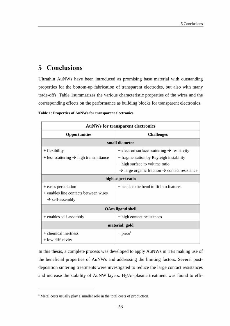
5 Conclusions
- 53 -
5 Conclusions
Ultrathin AuNWs have been introduced as promising base material with outstanding
properties for the bottom-up fabrication of transparent electrodes, but also with many
trade-offs. Table 1summarizes the various characteristic properties of the wires and the
corresponding effects on the performance as building blocks for transparent electronics.
Table 1: Properties of AuNWs for transparent electronics
In this thesis, a complete process was developed to apply AuNWs in TEs making use of
the beneficial properties of AuNWs and addressing the limiting factors. Several post-
deposition sintering treatments were investigated to reduce the large contact resistances
and increase the stability of AuNW layers. H2/Ar-plasma treatment was found to effi-
a Metal costs usually play a smaller role in the total costs of production.
AuNWs for transparent electronics
Opportunities Challenges
small diameter
+ flexibility − electron surface scattering resistivity
+ less scattering high transmittance − fragmentation by Rayleigh instability
− high surface to volume ratio
large organic fraction contact resistance
high aspect ratio
+ eases percolation − needs to be bend to fit into features
+ enables line contacts between wires
self-assembly
OAm ligand shell
+ enables self-assembly − high contact resistances
material: gold
+ chemical inertness
+ low diffusivity
− pricea
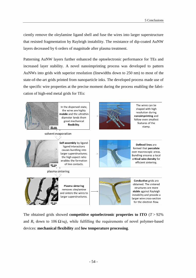
5 Conclusions
- 54 -
ciently remove the oleylamine ligand shell and fuse the wires into larger superstructure
that resisted fragmentation by Rayleigh instability. The resistance of dip-coated AuNW
layers decreased by 6 orders of magnitude after plasma treatment.
Patterning AuNW layers further enhanced the optoelectronic performance for TEs and
increased layer stability. A novel nanoimprinting process was developed to pattern
AuNWs into grids with superior resolution (linewidths down to 250 nm) to most of the
state-of-the-art grids printed from nanoparticle inks. The developed process made use of
the specific wire properties at the precise moment during the process enabling the fabri-
cation of high-end metal grids for TEs:
The obtained grids showed competitive optoelectronic properties to ITO (T > 92%
and Rs down to 106 Ω/sq), while fulfilling the requirements of novel polymer-based
devices: mechanical flexibility and low temperature processing.
6 Outlook
- 55 -
6 Outlook
Transparent electrode materials other than ITO are expected to represent a major part of
the entire TE market in the next decade.201
Although metal grids and metal nanowire
networks were shown to reach competitive properties to ITO, their breakthrough will
probably depend on how fast new applications like flexible devices that do not perform
with ITO will enter the market.
This thesis proved the usability of AuNWs as nanoscale building block for the fabrica-
tion of transparent and flexible metal grids. Future work could include:
Transfer the nanoimprinting process to continuous roll-to-roll processing. Ac-
companied with that, in-line sintering of the wires (for instance by atmospheric
plasma) would have to be investigated.
The combination of direct nanoimprinting and self-assembly of ultrathin wires is
not restricted to gold. The pivotal properties for the process are not intrinsic prop-
erties of gold, but are determined by the geometry and the specific ligand interac-
tions of the wires. Thus, exchange of the core material should not significantly af-
fect the printing process and could open up new opportunities.
The method could be extended to novel nanoparticle inks that are responsive to
external stimuli like light, magnetic fields or temperature in order to specifically
trigger the assembly during the imprinting process.
Future hierarchical printing processes could combine local nanoscale patterns (to
tune the material properties) with macroscopic circuit patterns in a single stamp.
Patterned electrodes, as required for capacitive touch screen, for instance, could
be fabricated in a single step. TEs like ITO or random AgNW layers have to be
patterned after layer deposition in an additional process step.

7 Bibliography
- 57 -
7 Bibliography
(1) Smartphone Usage Statistics 2014 - UK Survey of Smartphone Users | Tecmark
http://www.tecmark.co.uk/smartphone-usage-data-uk-2014/ (accessed Feb 7, 2017).
(2) Hecht, D. S.; Hu, L.; Irvin, G. Emerging Transparent Electrodes Based on Thin Films of Carbon
Nanotubes, Graphene, and Metallic Nanostructures. Adv. Mater. 2011, 23, 1482–1513.
(3) Ellmer, K. Past Achievements and Future Challenges in the Development of Optically
Transparent Electrodes. Nat. Photonics 2012, 6, 808–816.
(4) Morag, A.; Jelinek, R. “Bottom-Up” Transparent Electrodes. J. Colloid Interface Sci. 2016, 482,
267–289.
(5) Ye, S.; Rathmell, A. R.; Chen, Z.; Stewart, I. E.; Wiley, B. J. Metal Nanowire Networks: The
Next Generation of Transparent Conductors. Adv. Mater. 2014, 26, 6670–6687.
(6) Wright, A. W. On the Production of Transparent Metallic Film by the Electrical Discharge in
Exhausted Tubes. Am. J. Sci. 1877, 13, 49–55.
(7) Ghaffarzadeh, K.; Yamamoto, Y.; Zervos, H. Conductive Ink Markets 2016-2026: Forecasts,
Technologies, Players; IDTechEx Ltd: Boston, MA, USA, 2016.
(8) Progress in conductive ink-based transparent conductive films | Printed Electronics World
http://www.printedelectronicsworld.com/articles/10023/progress-in-conductive-ink-based-
transparent-conductive-films?rsst2id=1 (accessed Jan 2, 2017).
(9) Organic Solar Cells; Choy, W. C. H., Ed.; Green Energy and Technology; Springer London:
London, 2013.
(10) Brabec, C. J.; Sariciftci, N. S.; Hummelen, J. C. Plastic Solar Cells. Adv. Funtional Mater. 2001,
11, 15–26.
(11) Frohne, H.; Shaheen, S. E.; Brabec, C. J.; Müller, D. C.; Sariciftci, N. S.; Meerholz, K. Influence
of the Anodic Work Function on the Performance of Organic Solar Cells. ChemPhysChem 2002,
3, 795–799.
(12) OLED Info | The OLED Experts http://www.oled-info.com/ (accessed Jan 5, 2017).
(13) Sannicolo, T.; Lagrange, M.; Cabos, A.; Celle, C.; Simonato, J.-P.; Bellet, D. Metallic Nanowire-
Based Transparent Electrodes for Next Generation Flexible Devices: A Review. Small 2016, 12,
6052–6075.
(14) Gordon, R. G. Criteria for Choosing Transparent Conductors. MRS Bull. 2000, 52–57.
(15) Hu, L.; Wu, H.; Cui, Y. Metal Nanogrids, Nanowires, and Nanofibers for Transparent Electrodes.
MRS Bull. 2011, 36, 760–765.
(16) Gaynor, W.; Hofmann, S.; Christoforo, M. G.; Sachse, C.; Mehra, S.; Salleo, A.; McGehee, M.
D.; Gather, M. C.; Lüssem, B.; Müller-Meskamp, L.; et al. Color in the Corners: ITO-Free White
OLEDs with Angular Color Stability. Adv. Mater. 2013, 25, 4006–4013.
(17) Cravino, A.; Schilinsky, P.; Brabec, C. J. Characterization of Organic Solar Cells: The
Importance of Device Layout. Adv. Funct. Mater. 2007, 17, 3906–3910.
(18) Tvingstedt, K.; Inganäs, O. Electrode Grids for ITO-Free Organic Photovoltaic Devices. Adv.
Mater. 2007, 19, 2893–2897.
(19) Barnes, T. M.; Reese, M. O.; Bergeson, J. D.; Larsen, B. a.; Blackburn, J. L.; Beard, M. C.; Bult,
J.; van de Lagemaat, J. Comparing the Fundamental Physics and Device Performance of
7 Bibliography
- 58 -
Transparent, Conductive Nanostructured Networks with Conventional Transparent Conducting
Oxides. Adv. Energy Mater. 2012, 2, 353–360.
(20) Glover, R. E.; Tinkham, M. Conductivity of Superconducting Films for Photon Energies between
0.3 and 40kTc. Phys. Rev. 1957, 108, 243–256.
(21) Dressel, M.; Grüner, G. Electrodynamics of Solids: Optical Properties of Electrons in Matter;
Cambridge University Press, 2002.
(22) Hu, L.; Hecht, D. S.; Grüner, G. Percolation in Transparent and Conducting Carbon Nanotube
Networks. Nano Lett. 2004, 4, 2513–2517.
(23) De, S.; King, P. J.; Lyons, P. E.; Khan, U.; Coleman, J. N. Size Effects and the Problem with
Percolation in Nanostructured Transparent Conductors. ACS Nano 2010, 4, 7064–7072.
(24) Kim, T.; Canlier, A.; Cho, C.; Rozyyev, V.; Lee, J.; Han, S. M. Highly Transparent Au-Coated
Ag Nanowire Transparent Electrode with Reduction in Haze. ACS Appl. Mater. Interfaces 2014,
6, 13527–13534.
(25) Chiba, Y.; Islam, A.; Komiya, R.; Koide, N.; Han, L. Conversion Efficiency of 10.8% by a Dye-
Sensitized Solar Cell Using a TiO2 Electrode with High Haze. Appl. Phys. Lett. 2006, 88,
223505.
(26) Tang, Z.; Tress, W.; Inganäs, O. Light Trapping in Thin Film Organic Solar Cells. Mater. Today
2014, 17, 389–396.
(27) Araki, T.; Jiu, J.; Nogi, M.; Koga, H.; Nagao, S.; Sugahara, T.; Suganuma, K. Low Haze
Transparent Electrodes and Highly Conducting Air Dried Films with Ultra-Long Silver
Nanowires Synthesized by One-Step Polyol Method. Nano Res. 2014, 7, 236–245.
(28) Ok, K.-H.; Kim, J.; Park, S.-R.; Kim, Y.; Lee, C.-J.; Hong, S.-J.; Kwak, M.-G.; Kim, N.; Han, C.
J.; Kim, J.-W. Ultra-Thin and Smooth Transparent Electrode for Flexible and Leakage-Free
Organic Light-Emitting Diodes. Sci. Rep. 2015, 5, 9464.
(29) Nam, S.; Song, M.; Kim, D.-H.; Cho, B.; Lee, H. M.; Kwon, J.-D.; Park, S.-G.; Nam, K.-S.;
Jeong, Y.; Kwon, S.-H.; et al. Ultrasmooth, Extremely Deformable and Shape Recoverable Ag
Nanowire Embedded Transparent Electrode. Sci. Rep. 2014, 4, 4788.
(30) Kamyshny, A.; Magdassi, S. Conductive Nanomaterials for Printed Electronics. Small 2014, 10,
3515–3535.
(31) Drude, P. Zur Elektronentheorie Der Metalle. Ann. Phys. 1916, 354, 710–724.
(32) Zhang, L.; Zhou, Y.; Guo, L.; Zhao, W.; Barnes, A.; Zhang, H.-T.; Eaton, C.; Zheng, Y.; Brahlek,
M.; Haneef, H. F.; et al. Correlated Metals as Transparent Conductors. Nat. Mater. 2015, 15,
204–210.
(33) Hummel, R. E. Atomistic Theory of the Optical Properties. In Electronic Properties of Materials;
Springer New York: New York, NY, 2011; pp. 227–246.
(34) Dixon, S. C.; Scanlon, D. O.; Carmalt, C. J.; Parkin, I. P. N-Type Doped Transparent Conducting
Binary Oxides: An Overview. J. Mater. Chem. C 2016, 419, 462–465.
(35) Zilberberg, K.; Riedl, T. Metal-Nanostructures – A Modern and Powerful Platform to Create
Transparent Electrodes for Thin-Film Photovoltaics. J. Mater. Chem. A 2016, 4, 14481–14508.
(36) Edwards, P. P.; Porch, A.; Jones, M. O.; Morgan, D. V.; Perks, R. M. Basic Materials Physics of
Transparent Conducting Oxides. Dalton Trans. 2004, 2995–3002.
(37) Mizoguchi, H.; Kamiya, T.; Matsuishi, S.; Hosono, H. A Germanate Transparent Conductive
Oxide. Nat. Commun. 2011, 2, 470.
(38) Guo, C. F.; Ren, Z. Flexible Transparent Conductors Based on Metal Nanowire Networks. Mater.
Today 2015, 18, 143–154.
(39) Layani, M.; Kamyshny, A.; Magdassi, S. Transparent Conductors Composed of Nanomaterials.
Nanoscale 2014, 6, 5581–5591.
7 Bibliography
- 59 -
(40) Consolidation in transparent conductive film industry taking its toll | Printed Electronics World
http://www.printedelectronicsworld.com/articles/9078/consolidation-in-transparent-conductive-
film-industry-taking-its-toll (accessed Apr 28, 2017).
(41) ITO alternatives: printed metal mesh is on the rise? | IDTechEx Research Article
http://www.idtechex.com/research/articles/ito-alternatives-printed-metal-mesh-is-on-the-rise-
00010598.asp (accessed May 9, 2017).
(42) Hecht, D. S.; Kaner, R. B. Solution-Processed Transparent Electrodes. MRS Bull. 2011, 36, 749–
755.
(43) Heraeus. Conductive, Transparent and Flexible Polymers
https://www.heraeus.com/en/group/products_and_solutions_group/conductive_polymers/conducti
ve-polymers-home.aspx (accessed Jan 5, 2017).
(44) Kim, Y. H.; Sachse, C.; MacHala, M. L.; May, C.; Müller-Meskamp, L.; Leo, K. Highly
Conductive PEDOT:PSS Electrode with Optimized Solvent and Thermal Post-Treatment for
ITO-Free Organic Solar Cells. Adv. Funct. Mater. 2011, 21, 1076–1081.
(45) Huang, J.; Miller, P. F.; Wilson, J. S.; De Mello, A. J.; De Mello, J. C.; Bradley, D. D. C.
Investigation of the Effects of Doping and Post-Deposition Treatments on the Conductivity,
Morphology, and Work Function of poly(3,4- Ethylenedioxythiophene)/poly(styrene Sulfonate)
Films. Adv. Funct. Mater. 2005, 15, 290–296.
(46) Dimitriev, O. P.; Grinko, D. A.; Noskov, Y. V.; Ogurtsov, N. A.; Pud, A. A. PEDOT:PSS Films-
Effect of Organic Solvent Additives and Annealing on the Film Conductivity. Synth. Met. 2009,
159, 2237–2239.
(47) Tenent, R. C.; Barnes, T. M.; Bergeson, J. D.; Ferguson, A. J.; To, B.; Gedvilas, L. M.; Heben,
M. J.; Blackburn, J. L. UItrasmooth, Large-Area, High-Uniformity, Conductive Transparent
Single-Walled-Carbon-Nanotube Films for Photovoltaics Produced by Ultrasonic Spraying. Adv.
Mater. 2009, 21, 3210–3216.
(48) Dan, B.; Irvin, G. C.; Pasquali, M. Continuous and Scalable Fabrication of Transparent
Conducting Carbon Nanotube Films. ACS Nano 2009, 3, 835–843.
(49) Mirri, F.; Ma, A. W. K.; Hsu, T. T.; Behabtu, N.; Eichmann, S. L.; Young, C. C.; Tsentalovich,
D. E.; Pasquali, M. High-Performance Carbon Nanotube Transparent Conductive Films by
Scalable Dip Coating. ACS Nano 2012, 6, 9737–9744.
(50) Geim, A. K.; Novoselov, K. S. The Rise of Graphene. Nat. Mater. 2007, 6, 183–191.
(51) Wassei, J. K.; Kaner, R. B. Graphene, a Promising Transparent Conductor. Mater. Today 2010,
13, 52–59.
(52) Bae, S.; Kim, H.; Lee, Y.; Xu, X.; Park, J.-S.; Zheng, Y.; Balakrishnan, J.; Lei, T.; Ri Kim, H.;
Song, Y. Il; et al. Roll-to-Roll Production of 30-Inch Graphene Films for Transparent Electrodes.
Nat. Nanotechnol. 2010, 5, 574–578.
(53) Li, X. S.; Zhu, Y. W.; Cai, W. W.; Borysiak, M.; Han, B. Y.; Chen, D.; Piner, R. D.; Colombo,
L.; Ruoff, R. S. Transfer of Large-Area Graphene Films for High-Performance Transparent
Conductive Electrodes. Nano Lett. 2009, 9, 4359–4363.
(54) Polat, E. O.; Balci, O.; Kakenov, N.; Uzlu, H. B.; Kocabas, C.; Dahiya, R. Synthesis of Large
Area Graphene for High Performance in Flexible Optoelectronic Devices. Sci. Rep. 2015, 5,
16744.
(55) Chen, Y.; Gong, X. L.; Gai, J. G. Progress and Challenges in Transfer of Large-Area Graphene
Films. Adv. Sci. 2016, 3, 1–15.
(56) Dingle, R. B. The Electrical Conductivity of Thin Wires. Proc. R. Soc. London. Ser. A. Math.
Phys. Sci. 1950, 201, 545–560.
(57) Langley, D. P.; Lagrange, M.; Giusti, G.; Jiménez, C.; Bréchet, Y.; Nguyen, N. D.; Bellet, D.
Metallic Nanowire Networks: Effects of Thermal Annealing on Electrical Resistance. Nanoscale
2014, 6, 13535–13543.
7 Bibliography
- 60 -
(58) Mutiso, R. M.; Sherrott, M. C.; Rathmell, A. R.; Wiley, B. J.; Winey, K. I. Integrating
Simulations and Experiments to Predict Sheet Resistance and Optical Transmittance in Nanowire
Films for Transparent Conductors. ACS Nano 2013, 7, 7654–7663.
(59) Yu, Z.; Li, L.; Zhang, Q.; Hu, W.; Pei, Q. Silver Nanowire-Polymer Composite Electrodes for
Efficient Polymer Solar Cells. Adv. Mater. 2011, 23, 4453–4457.
(60) Scardaci, V.; Coull, R.; Lyons, P. E.; Rickard, D.; Coleman, J. N. Spray Deposition of Highly
Transparent, Low-Resistance Networks of Silver Nanowires over Large Areas. Small 2011, 7,
2621–2628.
(61) Hu, L.; Kim, H. S.; Lee, J.; Peumans, P.; Cui, Y. Scalable Coating and Properties of Transparent,
Flexible, Silver Nanowire Electrodes. ACS Nano 2010, 4, 2955–2963.
(62) Song, M.; You, D. S.; Lim, K.; Park, S.; Jung, S.; Kim, C. S.; Kim, D. H.; Kim, D. G.; Kim, J. K.;
Park, J.; et al. Highly Efficient and Bendable Organic Solar Cells with Solution-Processed Silver
Nanowire Electrodes. Adv. Funct. Mater. 2013, 23, 4177–4184.
(63) De, S.; Higgins, T. M.; Lyons, P. E.; Doherty, E. M.; Nirmalraj, P. N.; Blau, W. J.; Boland, J. J.;
Coleman, J. N. Silver Nanowire Networks as Flexible, Transparent, Conducting Films: Extremely
High DC to Optical Conductivity Ratios. ACS Nano 2009, 3, 1767–1774.
(64) Lee, P.; Lee, J.; Lee, H.; Yeo, J.; Hong, S.; Nam, K. H.; Lee, D.; Lee, S. S.; Ko, S. H. Highly
Stretchable and Highly Conductive Metal Electrode by Very Long Metal Nanowire Percolation
Network. Adv. Mater. 2012, 24, 3326–3332.
(65) Ye, S.; Stewart, I. E.; Chen, Z.; Li, B.; Rathmell, A. R.; Wiley, B. J. How Copper Nanowires
Grow and How to Control Their Properties. Acc. Chem. Res. 2016, 49, 442–451.
(66) Rathmell, A. R.; Wiley, B. J. The Synthesis and Coating of Long, Thin Copper Nanowires to
Make Flexible, Transparent Conducting Films on Plastic Substrates. Adv. Mater. 2011, 23, 4798–
4803.
(67) Rathmell, A. R.; Bergin, S. M.; Hua, Y.-L.; Li, Z.-Y.; Wiley, B. J. The Growth Mechanism of
Copper Nanowires and Their Properties in Flexible, Transparent Conducting Films. Adv. Mater.
2010, 22, 3558–3563.
(68) Chen, Z.; Ye, S.; Stewart, I. E.; Wiley, B. J. Copper Nanowire Networks with Transparent Oxide
Shells That Prevent Oxidation without Reducing Transmittance. ACS Nano 2014, 8, 9673–9679.
(69) Transparent Conductive Films (TCF) 2016-2026: Forecasts, Markets, Technologies: IDTechEx
http://www.idtechex.com/research/reports/transparent-conductive-films-tcf-2016-2026-forecasts-
markets-technologies-000480.asp (accessed Jan 23, 2017).
(70) Preston, C.; Xu, Y.; Han, X.; Munday, J. N.; Hu, L. Optical Haze of Transparent and Conductive
Silver Nanowire Films. Nano Res. 2013, 6, 461–468.
(71) Lee, J.-Y.; Connor, S. T.; Cui, Y.; Peumans, P. Solution-Processed Metal Nanowire Mesh
Transparent Electrodes. Nano Lett. 2008, 8, 689–692.
(72) Kumar, A.; Kulkarni, G. U. Evaluating Conducting Network Based Transparent Electrodes from
Geometrical Considerations. J. Appl. Phys. 2016, 119, 15102.
(73) Neyts, K.; Real, A.; Marescaux, M.; Mladenovski, S.; Beeckman, J. Conductor Grid Optimization
for Luminance Loss Reduction in Organic Light Emitting Diodes. J. Appl. Phys. 2008, 103,
93113.
(74) Catrysse, P. B.; Fan, S. Nanopatterned Metallic Films for Use as Transparent Conductive
Electrodes in Optoelectronic Devices. Nano Lett. 2010, 10, 2944–2949.
(75) Kuang, P.; Park, J. M.; Leung, W.; Mahadevapuram, R. C.; Nalwa, K. S.; Kim, T. G.; Chaudhary,
S.; Ho, K. M.; Constant, K. A New Architecture for Transparent Electrodes: Relieving the Trade-
off between Electrical Conductivity and Optical Transmittance. Adv. Mater. 2011, 23, 2469–
2473.
(76) Jang, S.; Jung, W.-B.; Kim, C.; Won, P.; Lee, S.-G.; Cho, K. M.; Jin, M. liang; An, C. J.; Jeon,
H.-J.; Ko, S. H.; et al. A Three-Dimensional Metal Grid Mesh as a Practical Alternative to ITO.
7 Bibliography
- 61 -
Nanoscale 2016, 8, 14257–14263.
(77) Van De Groep, J.; Spinelli, P.; Polman, A. Transparent Conducting Silver Nanowire Networks.
Nano Lett. 2012, 12, 3138–3144.
(78) Liu, W.; Fang, Y.; Xu, Y. F.; Li, X.; Li, L. H. The Effect of Grid Shape on the Properties of
Transparent Conductive Films Based on Flexographic Printing. Sci. China Technol. Sci. 2014, 57,
2536–2541.
(79) Bergin, S. M.; Chen, Y.-H.; Rathmell, A. R.; Charbonneau, P.; Li, Z.-Y.; Wiley, B. J. The Effect
of Nanowire Length and Diameter on the Properties of Transparent, Conducting Nanowire Films.
Nanoscale 2012, 4, 1996.
(80) Lee, S.-M.; Chae, J.-S.; Kim, D.-Y.; Choi, K. C. Plasmonic Nanomeshes as Large-Area, Low-
Resistive Transparent Electrodes and Their Application to ITO-Free Organic Light-Emitting
Diodes. Org. Electron. 2014, 15, 3354–3361.
(81) Wu, W.; Tassi, N. G. A Broadband Plasmonic Enhanced Transparent Conductor. Nanoscale
2014, 6, 7811–7816.
(82) Lim, J. W.; Lee, Y. T.; Pandey, R.; Yoo, T.-H.; Sang, B.-I.; Ju, B.-K.; Hwang, D. K.; Choi, W. K.
Effect of Geometric Lattice Design on Optical/electrical Properties of Transparent Silver Grid for
Organic Solar Cells. Opt. Express 2014, 22, 26891.
(83) Zou, J.; Yip, H.-L.; Hau, S. K.; Jen, A. K.-Y. Metal Grid/conducting Polymer Hybrid Transparent
Electrode for Inverted Polymer Solar Cells. Appl. Phys. Lett. 2010, 96, 203301.
(84) Wünscher, S.; Abbel, R.; Perelaer, J.; Schubert, U. S. Progress of Alternative Sintering
Approaches of Inkjet-Printed Metal Inks and Their Application for Manufacturing of Flexible
Electronic Devices. J. Mater. Chem. C 2014, 2, 10232–10261.
(85) Ahn, B. Y.; Lorang, D. J.; Lewis, J. A. Transparent Conductive Grids via Direct Writing of Silver
Nanoparticle Inks. Nanoscale 2011, 3, 2700–2702.
(86) Jang, Y.; Kim, J.; Byun, D. Invisible Metal-Grid Transparent Electrode Prepared by
Electrohydrodynamic (EHD) Jet Printing. J. Phys. D. Appl. Phys. 2013, 46, 155103.
(87) Park, J.; Hwang, J. Fabrication of a Flexible Ag-Grid Transparent Electrode Using Ac Based
Electrohydrodynamic Jet Printing. J. Phys. D. Appl. Phys. 2014, 47, 405102.
(88) Schneider, J.; Rohner, P.; Thureja, D.; Schmid, M.; Galliker, P.; Poulikakos, D.
Electrohydrodynamic NanoDrip Printing of High Aspect Ratio Metal Grid Transparent
Electrodes. Adv. Funct. Mater. 2015, 26, 833–840.
(89) Hong, S.; Yeo, J.; Kim, G.; Kim, D.; Lee, H.; Kwon, J.; Lee, H.; Lee, P.; Ko, S. H. Nonvacuum,
Maskless Fabrication of a Flexible Metal Grid Transparent Conductor by Low-Temperature
Selective Laser Sintering of Nanoparticle Ink. ACS Nano 2013, 7, 5024–5031.
(90) Lee, D.; Paeng, D.; Park, H. K.; Grigoropoulos, C. P. Vacuum-Free, Maskless Patterning of Ni
Electrodes by Laser Reductive Sintering of NiO Nanoparticle Ink and Its Application to
Transparent Conductors. ACS Nano 2014, 8, 9807–9814.
(91) Layani, M.; Gruchko, M.; Milo, O.; Balberg, I.; Azulay, D.; Magdassi, S. Transparent Conductive
Coatings by Printing Coffee Ring Arrays Obtained at Room Temperature. ACS Nano 2009, 3,
3537–3542.
(92) Deegan, R. D.; Bakajin, O.; Dupont, T. F. Capillary Flow as the Cause of Ring Stains from Dried
Liquid Drops. Nature 1997, 389, 827–829.
(93) Zhang, Z.; Zhang, X.; Xin, Z.; Deng, M.; Wen, Y.; Song, Y. Controlled Inkjetting of a
Conductive Pattern of Silver Nanoparticles Based on the Coffee-Ring Effect. Adv. Mater. 2013,
25, 6714–6718.
(94) Zhang, Z.; Zhu, W. Controllable Fabrication of a Flexible Transparent Metallic Grid Conductor
Based on the Coffee Ring Effect. J. Mater. Chem. C 2014, 2, 9587–9591.
(95) Higashitani, K.; McNamee, C. E.; Nakayama, M. Formation of Large-Scale Flexible Transparent
7 Bibliography
- 62 -
Conductive Films Using Evaporative Migration Characteristics of Au Nanoparticles. Langmuir
2011, 27, 2080–2083.
(96) Layani, M.; Magdassi, S. Flexible Transparent Conductive Coatings by Combining Self-
Assembly with Sintering of Silver Nanoparticles Performed at Room Temperature. J. Mater.
Chem. 2011, 21, 15378.
(97) Magdassi, S.; Grouchko, M.; Berezin, O.; Kamyshny, A. Triggering the Sintering of Silver
Nanoparticles at Room Temperature. ACS Nano 2010, 4, 1943–1948.
(98) Malaquin, L.; Kraus, T.; Schmid, H.; Delamarche, E.; Wolf, H. Controlled Particle Placement
through Convective and Capillary Assembly. Langmuir 2007, 23, 11513–11521.
(99) Kim, H. S.; Lee, C. H.; Sudeep, P. K.; Emrick, T.; Crosby, A. J. Nanoparticle Stripes, Grids, and
Ribbons Produced by Flow Coating. Adv. Mater. 2010, 22, 4600–4604.
(100) Park, J. H.; Lee, D. Y.; Seung, W.; Sun, Q.; Kim, S.-W.; Cho, J. H. Metallic Grid Electrode
Fabricated via Flow Coating for High-Performance Flexible Piezoelectric Nanogenerators. J.
Phys. Chem. C 2015, 119, 7802–7808.
(101) Winzer, M.; Kleiber, M.; Dix, N.; Wiesendanger, R. Fabrication of Nano-Dot- and Nano-Ring-
Arrays by Nanosphere Lithography. Appl. Phys. A Mater. Sci. Process. 1996, 63, 617–619.
(102) Ho, Y. H.; Chen, K. Y.; Liu, S. W.; Chang, Y. T.; Huang, D. W.; Wei, P. K. Transparent and
Conductive Metallic Electrodes Fabricated by Using Nanosphere Lithography. Org. Electron.
2011, 12, 961–965.
(103) Kwon, N.; Kim, K.; Sung, S.; Yi, I.; Chung, I. Highly Conductive and Transparent Ag
Honeycomb Mesh Fabricated Using a Monolayer of Polystyrene Spheres. Nanotechnology 2013,
24, 235205.
(104) Kwon, N.; Kim, K.; Heo, J.; Yi, I.; Chung, I. Study on Ag Mesh/ Conductive Oxide Hybrid
Transparent Electrode for Film Heaters. Nanotechnology 2014, 25, 265702.
(105) Kang, M. G.; Kim, M. S.; Kim, J. S.; Guo, L. J. Organic Solar Cells Using Nanoimprinted
Transparent Metal Electrodes. Adv. Mater. 2008, 20, 4408–4413.
(106) Transparent Conductive Films (TCF) 2015-2025: Forecasts, Markets, Technologies | Acute
Market Reports http://www.acutemarketreports.com/report/transparent-conductive-films-tcf-
2015-2025-forecasts-markets-technologies (accessed Jan 24, 2017).
(107) Schift, H.; Kristensen, A. Nanoimprint Lithography. In Springer Handbook of Nanotechnology;
Bhushan, B., Ed.; Springer Berlin Heidelberg, 2007; pp. 239–278.
(108) Lan, H.; Ding, Y. Nanoimprint Lithography. In Lithography; Wang, M., Ed.; InTech, 2010; pp.
457–494.
(109) Guo, L. J. Nanoimprint Lithography: Methods and Material Requirements. Adv. Mater. 2007, 19,
495–513.
(110) Zhou, W. Nanoimprint Lithography: An Enabling Process for Nanofabrication; Springer Berlin
Heidelberg, 2013.
(111) Guo, L. J. Patterning Based on External Force: Nanoimprint Lithography. In Unconventional
Nanopatterning Techniques and Applications; Rogers, J. A.; Lee, H. H., Eds.; John Wiley &
Sons, Inc., 2008; pp. 129–166.
(112) Ahn, S. H.; Guo, L. J. Large-Area Roll-to-Roll and Roll-to-Plate Nanoimprint Lithography : A
Step toward High-Throughput Application of Continuous Nanoimprinting. ACS Nano 2009, 3,
2304–2310.
(113) Ahn, S. H.; Guo, L. J. High-Speed Roll-to-Roll Nanoimprint Lithography on Flexible Plastic
Substrates. Adv. Mater. 2008, 20, 2044–2049.
(114) Stuart, C.; Chen, Y. Roll in and Roll out: A Path to High-Throughput Nanoimprint Lithography.
ACS Nano 2009, 3, 2062–2064.
7 Bibliography
- 63 -
(115) TEMICOAT - NANOIMPRINT TECHNOLOGIES http://www.temicoat.com/ (accessed Jan 16,
2017).
(116) Xia, Y.; Whitesides, G. M. Soft Lithography. Annu. Rev. Mater. Sci. 1998, 28, 153–184.
(117) Qin, D.; Xia, Y.; Whitesides, G. M. Soft Lithography for Micro- and Nanoscale Patterning. Nat.
Protoc. 2010, 5, 491–502.
(118) Qin, D.; Xia, Y.; Whitesides, G. M. Soft Lithography for Micro- and Nanoscale Patterning. Nat.
Protoc. 2010, 5, 491–502.
(119) Cavallini, M.; Albonetti, C.; Biscarini, F. Nanopatterning Soluble Multifunctional Materials by
Unconventional Wet Lithography. Adv. Mater. 2009, 21, 1043–1053.
(120) Moonen, P. F.; Bat, E.; Voorthuijzen, W. P.; Huskens, J. Soft-Lithographic Patterning of Room
Temperature-Sintering Ag Nanoparticles on Foil. RSC Adv. 2013, 3, 18498.
(121) Duan, X.; Park, M.; Zhao, Y.; Berenschot, E.; Wang, Z.; Reinhoudt, D. N.; Rotello, V. M.;
Huskens, J. Metal Nanoparticle Wires Formed by an Integrated Nanomolding-Chemical
Assembly Process : Fabrication and Properties. ACS Nano 2010, 4, 7660–7666.
(122) Kim, E.; Xia, Y.; Whitesides, G. M. Micromolding in Capillaries: Applications in Materials
Science. J. Am. Chem. Soc. 1996, 118, 5722–5731.
(123) Ko, S. H.; Park, I.; Pan, H.; Grigoropoulos, C. P.; Pisano, A. P.; Luscombe, C. K.; Fréchet, J. M.
J. Direct Nanoimprinting of Metal Nanoparticles for Nanoscale Electronics Fabrication. Nano
Lett. 2007, 7, 1869–1877.
(124) Liang, C.-C.; Liao, M.-Y.; Chen, W.-Y.; Cheng, T.-C.; Chang, W.-H.; Lin, C.-H. Plasmonic
Metallic Nanostructures by Direct Nanoimprinting of Gold Nanoparticles. Opt. Express 2011, 19,
4768–4776.
(125) Fafarman, A. T.; Hong, S.-H.; Caglayan, H.; Ye, X.; Diroll, B. T.; Paik, T.; Engheta, N.; Murray,
C. B.; Kagan, C. R. Chemically Tailored Dielectric-to-Metal Transition for the Design of
Metamaterials from Nanoimprinted Colloidal Nanocrystals. Nano Lett. 2013, 13, 350–357.
(126) Park, I.; Ko, S. H.; Pan, H.; Grigoropoulos, C. P.; Pisano, A. P.; Fréchet, J. M. J.; Lee, E.-S.;
Jeong, J.-H. Nanoscale Patterning and Electronics on Flexible Substrate by Direct
Nanoimprinting of Metallic Nanoparticles. Adv. Mater. 2008, 20, 489–496.
(127) Hu, P.; Li, K.; Chen, W.; Peng, L.; Chu, D.; O’Neill, W. Fabrication of an Organic Field Effect
Transistor Using Nano Imprinting of Ag Inks and Semiconducting Polymers. J. Micromechanics
Microengineering 2010, 20, 129802.
(128) Yu, X.; Pham, J. T.; Subramani, C.; Creran, B.; Yeh, Y.-C.; Du, K.; Patra, D.; Miranda, O. R.;
Crosby, A. J.; Rotello, V. M. Direct Patterning of Engineered Ionic Gold Nanoparticles via
Nanoimprint Lithography. Adv. Mater. 2012, 24, 6330–6334.
(129) Kim, J. Y.; Kotov, N. A. Charge Transport Dilemma of Solution-Processed Nanomaterials.
Chem. Mater. 2014, 26, 134–152.
(130) Boles, M. A.; Engel, M.; Talapin, D. V. Self-Assembly of Colloidal Nanocrystals: From Intricate
Structures to Functional Materials. Chem. Rev. 2016, 116, 11220–11289.
(131) Reiser, B.; Gonzalez-Garcia, L.; Kanelidis, I.; Maurer, J. H. M.; Kraus, T. Gold Nanorods with
Conjugated Polymer Ligands: Sintering-Free Conductive Inks for Printed Electronics. Chem. Sci.
2016, 7, 4190–4196.
(132) Yang, C.; Wong, C. P.; Yuen, M. M. F. Printed Electrically Conductive Composites: Conductive
Filler Designs and Surface Engineering. J. Mater. Chem. C 2013, 1, 4052.
(133) Roduner, E. Size Matters: Why Nanomaterials Are Different. Chem. Soc. Rev. 2006, 35, 583.
(134) Qi, W. H.; Wang, M. P. Size and Shape Dependent Melting Temperature of Metallic
Nanoparticles. Mater. Chem. Phys. 2004, 88, 280–284.
(135) Buffat, P.; Borel, J. P. Size Effect on the Melting Temperature of Gold Particles. Phys. Rev. A
7 Bibliography
- 64 -
1976, 13, 2287–2298.
(136) Cherrington, M.; Claypole, T. C.; Deganello, D.; Mabbett, I.; Watson, T.; Worsley, D. Ultrafast
near-Infrared Sintering of a Slot-Die Coated Nano-Silver Conducting Ink. J. Mater. Chem. 2011,
21, 7562–7564.
(137) NIR-Technologie, Lösungen, Anwendungen und Trockner - Adphos Gruppe
http://www.adphos.com/de/ (accessed Jan 12, 2017).
(138) Schroder, K. A.; McCool, S. C.; Furlan, W. F. Broadcast Photonic Curing of Metallic
Nanoparticle Films. NSTI-Nanotech 2006, 3, 198–201.
(139) Hwang, Y. T.; Chung, W.-H.; Jang, Y. R.; Kim, H.-S. Intensive Plasmonic Flash Light Sintering
of Copper Nano-Inks Using a Band-Pass Light Filter for Highly Electrically Conductive
Electrodes in Printed Electronics. ACS Appl. Mater. Interfaces 2016, 8, 8591–8599.
(140) Niittynen, J.; Sowade, E.; Kang, H.; Baumann, R. R.; Mäntysalo, M. Comparison of Laser and
Intense Pulsed Light Sintering (IPL) for Inkjet-Printed Copper Nanoparticle Layers. Sci. Rep.
2015, 5, 8832.
(141) Garnett, E. C.; Cai, W.; Cha, J. J.; Mahmood, F.; Connor, S. T.; Greyson Christoforo, M.; Cui,
Y.; McGehee, M. D.; Brongersma, M. L. Self-Limited Plasmonic Welding of Silver
Nanowire Junctions. Nat. Mater. 2012, 11, 241–249.
(142) Jiu, J.; Nogi, M.; Sugahara, T.; Tokuno, T.; Araki, T.; Komoda, N.; Suganuma, K.; Uchida, H.;
Shinozaki, K. Strongly Adhesive and Flexible Transparent Silver Nanowire Conductive Films
Fabricated with a High-Intensity Pulsed Light Technique. J. Mater. Chem. 2012, 22, 23561.
(143) Park, S.-H.; Jang, S.; Lee, D.-J.; Oh, J.; Kim, H.-S. Two-Step Flash Light Sintering Process for
Crack-Free Inkjet-Printed Ag Films. J. Micromechanics Microengineering 2013, 23, 15013.
(144) Lee, D. J.; Park, S. H.; Jang, S.; Kim, H. S.; Oh, J. H.; Song, Y. W. Pulsed Light Sintering
Characteristics of Inkjet-Printed Nanosilver Films on a Polymer Substrate. J. Micromechanics
Microengineering 2011, 21, 125023.
(145) Printed Electronics Product Leadership | NovaCentrix
http://www.novacentrix.com/products/overview (accessed Jan 12, 2017).
(146) Gepulste Blitzlampen - Xenon und Krypton
https://www.heraeus.com/de/hng/products_and_solutions/arc_and_flash_lamps/flash_lamps.aspx
(accessed Jan 12, 2017).
(147) Schroder, K. a; Suite, P. D. Mechanisms of Photonic CuringTM
: Processing High Temperature
Films on Low Temperature Substrates. Nanotech Conf. Tech. Proc. 2011, 220–223.
(148) Pilot Scale Roll to Roll | NovaCentrix http://www.novacentrix.com/products/pulseforge/R2R
(accessed Jan 12, 2017).
(149) Yung, K. C.; Gu, X.; Lee, C. P.; Choy, H. S. Ink-Jet Printing and Camera Flash Sintering of
Silver Tracks on Different Substrates. J. Mater. Process. Technol. 2010, 210, 2268–2272.
(150) Ko, S. H.; Pan, H.; Grigoropoulos, C. P.; Luscombe, C. K.; Fréchet, J. M. J.; Poulikakos, D. All-
Inkjet-Printed Flexible Electronics Fabrication on a Polymer Substrate by Low-Temperature
High-Resolution Selective Laser Sintering of Metal Nanoparticles. Nanotechnology 2007, 18,
345202.
(151) Grouchko, M.; Kamyshny, A.; Mihailescu, C. F.; Anghel, D. F.; Magdassi, S. Conductive Inks
with A “built-In” mechanism That Enables Sintering at Room Temperature. ACS Nano 2011, 5,
3354–3359.
(152) Fafarman, A. T.; Koh, W.; Diroll, B. T.; Kim, D. K.; Ko, D.-K.; Oh, S. J.; Ye, X.; Doan-Nguyen,
V.; Crump, M. R.; Reifsnyder, D. C.; et al. Thiocyanate-Capped Nanocrystal Colloids :
Vibrational Reporter of Surface Chemistry and Solution-Based Route to Enhanced Coupling in
Nanocrystal Solids. J. Am. Chem. Soc. 2011, 133, 15753–15761.
(153) Korner, N.; Beck, E.; Dommann, A.; Onda, N.; Ramm, J. Hydrogen Plasma Chemical Cleaning
of Metallic Substrates and Silicon Wafers. Surf. Coatings Technol. 1995, 76–77, 731–737.
7 Bibliography
- 65 -
(154) Gehl, B.; Frömsdorf, A.; Aleksandrovic, V.; Schmidt, T.; Pretorius, A.; Flege, J.-I.; Bernstorff, S.;
Rosenauer, A.; Falta, J.; Weller, H.; et al. Structural and Chemical Effects of Plasma Treatment
on Close-Packed Colloidal Nanoparticle Layers. Adv. Funct. Mater. 2008, 18, 2398–2410.
(155) Reinhold, I.; Hendriks, C. E.; Eckardt, R.; Kranenburg, J. M.; Perelaer, J.; Baumann, R. R.;
Schubert, U. S. Argon Plasma Sintering of Inkjet Printed Silver Tracks on Polymer Substrates. J.
Mater. Chem. 2009, 19, 3384–3388.
(156) Cademartiri, L.; Ghadimi, A.; Ozin, G. A. Nanocrystal Plasma Polymerization : From Colloidal
Nanocrystals to Inorganic Architectures. Acc. Chem. Res. 2008, 41, 1820–1830.
(157) Wünscher, S.; Stumpf, S.; Teichler, A.; Pabst, O.; Perelaer, J.; Beckert, E.; Schubert, U. S.
Localized Atmospheric Plasma Sintering of Inkjet Printed Silver Nanoparticles. J. Mater. Chem.
2012, 22, 24569–24576.
(158) Zhang, A.; Zheng, G.; Lieber, C. Nanowires : Building Blocks for Nanoscience and
Nanotechnology; Springer International Publishing, 2016.
(159) Pei, L.; Mori, K.; Adachi, M. Formation Process of Two-Dimensional Networked Gold
Nanowires by Citrate Reduction of AuCl4- and the Shape Stabilization. Langmuir 2004, 20,
7837–7843.
(160) Kim, F.; Sohn, K.; Wu, J.; Huang, J. Chemical Synthesis of Gold Nanowires in Acidic Solutions.
J. Am. Chem. Soc. 2008, 130, 14442–14443.
(161) Liu, X.; Wu, N.; Wunsch, B. H.; Barsotti, R. J.; Stellacci, F. Shape-Controlled Growth of
Micrometer-Sized Gold Crystals by a Slow Reduction Method. Small 2006, 2, 1046–1050.
(162) Bai, H.; Xu, K.; Xu, Y.; Matsui, H. Fabrication of Au Nanowires of Uniform Length and
Diameter Using a Monodisperse and Rigid Biomolecular Template: Collagen-like Triple Helix.
Angew. Chemie - Int. Ed. 2007, 46, 3319–3322.
(163) Forrer, P.; Schlottig, F.; Siegenthaler, H.; Textor, M. Electrochemical Preparation and Surface
Properties of Gold Nanowire Arrays Formed by the Template Technique. J. Appl. Electrochem.
2000, 30, 533–541.
(164) Cross, C. E.; Hemminger, J. C.; Penner, R. M. Physical Vapor Deposition of One-Dimensional
Nanoparticle Arrays on Graphite: Seeding the Electrodeposition of Gold Nanowires. Langmuir
2007, 23, 10372–10379.
(165) Halder, A.; Ravishankar, N. Ultrafine Single-Crystalline Gold Nanowire Arrays by Oriented
Attachment. Adv. Mater. 2007, 19, 1854–1858.
(166) Wang, C.; Hu, Y.; Lieber, C. M.; Sun, S. Ultrathin Au Nanowires and Their Transport Properties.
J. Am. Chem. Soc. 2008, 130, 8902–8903.
(167) Huo, Z.; Tsung, C.-K.; Huang, W.; Zhang, X.; Yang, P. Sub-Two Nanometer Single Crystal Au
Nanowires. Nano Lett. 2008, 8, 2041–2044.
(168) Pazos-Pérez, N.; Baranov, D.; Irsen, S.; Hilgendorff, M.; Liz-Marzán, L. M.; Giersig, M.
Synthesis of Flexible, Ultrathin Gold Nanowires in Organic Media. Langmuir 2008, 24, 9855–
9860.
(169) Lu, X.; Yavuz, M. S.; Tuan, H.; Korgel, B. A.; Xia, Y. Ultrathin Gold Nanowires Can Be
Obtained by Reducing Polymeric Strands of Oleylamine - AuCl Complexes Formed via
Aurophilic Interaction. J. Am. Chem. Soc. 2008, 130, 8900–8901.
(170) Feng, H.; Yang, Y.; You, Y.; Li, G.; Guo, J.; Yu, T.; Shen, Z.; Wu, T.; Xing, B. Simple and
Rapid Synthesis of Ultrathin Gold Nanowires, Their Self-Assembly and Application in Surface-
Enhanced Raman Scattering. Chem. Commun. 2009, 1984–1986.
(171) Pong, B. K.; Lee, J. Y.; Trout, B. L. First Principles Computational Study for Understanding the
Interactions between ssDNA and Gold Nanoparticles: Adsorption of Methylamine on Gold
Nanoparticulate Surfaces. Langmuir 2005, 21, 11599–11603.
(172) You, H.; Liu, X.; Liu, H.; Fang, J. Theoretical Description of the Role of Amine Surfactant on the
Anisotropic Growth of Gold Nanocrystals. CrystEngComm 2016, 18, 3934–3941.
7 Bibliography
- 66 -
(173) You, H.; Wang, W.; Yang, S. A Universal Rule for Organic Ligand Exchange. ACS Appl. Mater.
Interfaces 2014, 6, 19035–19040.
(174) Wang, C.; Hou, Y.; Kim, J.; Sun, S. A General Strategy for Synthesizing FePt Nanowires and
Nanorods. Angew. Chemie - Int. Ed. 2007, 46, 6333–6335.
(175) Loubat, A.; Impéror-Clerc, M.; Pansu, B.; Meneau, F.; Raquet, B.; Viau, G.; Lacroix, L.-M.
Growth and Self-Assembly of Ultrathin Au Nanowires into Expanded Hexagonal Superlattice
Studied by in Situ SAXS. Langmuir 2014, 30, 4005–4012.
(176) Yu, Y.; Cui, F.; Sun, J.; Yang, P. Atomic Structure of Ultrathin Gold Nanowires. Nano Lett.
2016, 16, 3078–3084.
(177) Sánchez-Iglesias, A.; Rivas-Murias, B.; Grzelczak, M.; Pérez-Juste, J.; Liz-Marzán, L. M.;
Rivadulla, F.; Correa-Duarte, M. A. Highly Transparent and Conductive Films of Densely
Aligned Ultrathin Au Nanowire Monolayers. Nano Lett. 2012, 12, 6066–6070.
(178) Chen, Y.; Ouyang, Z.; Gu, M.; Cheng, W. Mechanically Strong, Optically Transparent, Giant
Metal Superlattice Nanomembranes from Ultrathin Gold Nanowires. Adv. Mater. 2013, 25, 80–
85.
(179) Reiser, B.; Gerstner, D.; Gonzalez-Garcia, L.; Maurer, J. H. M.; Kanelidis, I.; Kraus, T.
Multivalent Bonds in Self-Assembled Bundles of Ultrathin Gold Nanowires. Phys. Chem. Chem.
Phys. 2016, 18, 27165–27169.
(180) Gong, S.; Schwalb, W.; Wang, Y.; Chen, Y.; Tang, Y.; Si, J.; Shirinzadeh, B.; Cheng, W. A
Wearable and Highly Sensitive Pressure Sensor with Ultrathin Gold Nanowires. Nat. Commun.
2014, 5, 1–8.
(181) Gong, S.; Lai, D. T. H.; Su, B.; Si, K. J.; Ma, Z.; Yap, L. W.; Guo, P.; Cheng, W. Highly Stretchy
Black Gold E-Skin Nanopatches as Highly Sensitive Wearable Biomedical Sensors. Adv.
Electron. Mater. 2015, 1, 1400063.
(182) Gong, S.; Lai, D. T. H.; Wang, Y.; Yap, L. W.; Si, K. J.; Shi, Q.; Jason, N. N.; Sridhar, T.; Uddin,
H.; Cheng, W. Tattoolike Polyaniline Microparticle-Doped Gold Nanowire Patches as Highly
Durable Wearable Sensors. ACS Appl. Mater. Interfaces 2015, 7, 19700–19708.
(183) Pud, S.; Kisner, A.; Heggen, M.; Belaineh, D.; Temirov, R.; Simon, U.; Offenhäusser, A.;
Mourzina, Y.; Vitusevich, S. Features of Transport in Ultrathin Gold Nanowire Structures. Small
2013, 9, 846–852.
(184) Sondheimer, E. H. The Mean Free Path of Electrons in Metals. Adv. Phys. 1952, 1, 1–42.
(185) Plateau, J. . Transl. Annu. Reports Smithson. Inst. 1873, 1863.
(186) Rayleigh, Lord. On the Stability of Jets. Proc. London Math. Soc. 1878, 10, 4–12.
(187) Nichols, F.A.; Mullins, W. W. Surface- (Interface-) and Volume-Diffusion Contribution to
Morphological Changes Driven by Capillarity. Trans. Met. Soc. AIME 1965, 233, 1840–1848.
(188) Karim, S.; Toimil-Molares, M. E.; Balogh, A. G.; Ensinger, W.; Cornelius, T. W.; Khan, E. U.;
Neumann, R. Morphological Evolution of Au Nanowires Controlled by Rayleigh Instability.
Nanotechnology 2006, 17, 5954–5959.
(189) Toimil Molares, M. E.; Balogh, A. G.; Cornelius, T. W.; Neumann, R.; Trautmann, C.
Fragmentation of Nanowires Driven by Rayleigh Instability. Appl. Phys. Lett. 2004, 85, 5337–
5339.
(190) Xu, J.; Zhu, Y.; Zhu, J.; Jiang, W. Ultralong Gold Nanoparticle/block Copolymer Hybrid
Cylindrical Micelles: A Strategy Combining Surface Templated Self-Assembly and Rayleigh
Instability. Nanoscale 2013, 5, 6344–6349.
(191) Lacroix, L. M.; Arenal, R.; Viau, G. Dynamic HAADF-STEM Observation of a Single-Atom
Chain as the Transient State of Gold Ultrathin Nanowire Breakdown. J. Am. Chem. Soc. 2014,
136, 13075–13077.
(192) Gonzalez-Garcia, L.; Maurer, J. H. M.; Reiser, B.; Kanelidis, I.; Kraus, T. Ultrathin Gold
7 Bibliography
- 67 -
Nanowires for Transparent Electronics: Breaking Barriers. Procedia Eng. 2016, 141, 152–156.
(193) Gong, S.; Zhao, Y.; Yap, L. W.; Shi, Q.; Wang, Y.; Bay, J. A. P. B.; Lai, D. T. H.; Uddin, H.;
Cheng, W. Fabrication of Highly Transparent and Flexible NanoMesh Electrode via Self-
Assembly of Ultrathin Gold Nanowires. Adv. Electron. Mater. 2016, 1600121.
(194) He, Y.; Chen, Y.; Xu, Q.; Xu, J.; Weng, J. Assembly of Ultrathin Gold Nanowires into
Honeycomb Macroporous Pattern Films with High Transparency and Conductivity. ACS Appl.
Mater. Interfaces 2017, 9, 7826–7833.
(195) Takahata, R.; Yamazoe, S.; Warakulwit, C.; Limtrakul, J.; Tsukuda, T. Rayleigh Instability and
Surfactant-Mediated Stabilization of Ultrathin Gold Nanorods. J. Phys. Chem. C 2016, 120,
17006–17010.
(196) Huber, S. E.; Warakulwit, C.; Limtrakul, J.; Tsukuda, T.; Probst, M. Thermal Stabilization of
Thin Gold Nanowires by Surfactant-Coating: A Molecular Dynamics Study. Nanoscale 2012, 4,
585–590.
(197) Thompson, C. V. Solid-State Dewetting of Thin Films. Annu. Rev. Mater. Res. 2012, 42, 399–
434.
(198) Hernadez-Cruz, O.; Avila-Gutierrez, L.; Zolotukhin, M. G.; Gonzalez, G.; Monroy, B. M.;
Montiel, R.; Vera-Graziano, R.; Romero-Ibarra, J. E.; Novelo-Peralta, O.; Massoojas, F. A.
Spontaneous, Solvent-Free, Polymer-Templated, Solid−Solid Transformation of Thin Metal
Films into Nanoparticles. Nano Lett. 2016, 16, 5420–5425.
(199) Müller, C. M.; Spolenak, R. Microstructure Evolution during Dewetting in Thin Au Films. Acta
Mater. 2010, 58, 6035–6045.
(200) Backes, I. K. Large-Area Nanoimprint of Ultrathin Gold Nanowires: Ink-Stamp Interplay,
Saarland University and INM - Leibniz Institute for New Materials, 2016.
(201) Transparent Conductive Films (TCF) 2017-2027: Forecasts, Markets, Technologies: IDTechEx
http://www.idtechex.com/research/reports/transparent-conductive-films-tcf-2017-2027-forecasts-
markets-technologies-000524.asp (accessed May 10, 2017).
(202) Saw, K. G.; Aznan, N. M.; Yam, F. K.; Ng, S. S.; Pung, S. Y. New Insights on the Burstein-Moss
Shift and Band Gap Narrowing in Indium-Doped Zinc Oxide Thin Films. PLoS One 2015, 10, 1–
17.
(203) Hamberg, I.; Granqvist, C. G.; Berggren, K. F.; Sernelius, B. E.; Engstr??m, L. Band-Gap
Widening in Heavily Sn-Doped In2O3. Phys. Rev. B 1984, 30, 3240–3249.

8 Appendix
- 69 -
8 Appendix
8.1 List of abbreviations and symbols
AFM Atomic force microscope
AgNP(s) Silver nanoparticle(s)
AuNP(s) Gold nanoparticle(s)
AgNW(s) Silver nanowire(s)
AuNW(s) Gold nanowire(s)
CuNW(s) Copper nanowire(s)
GISAXS Gracing-incidence small-angle X-ray scattering
h Planck's constant
ITO Indium tin oxide
LED Light-emitting diode
NIR Near-infrared
NM Nanomesh
NP(s) Nanoparticle(s)
OAm Oleylamine
OLED(s) Organic light-emitting diode(s)
OSC(s) Organic solar cell(s)
PDMS Polydimethylsiloxane
PEDOT:PSS Poly(3,4-ethylenedioxythiophene):poly(styrenesulfonate)
PET Polyethylene terephthalate
PTEBS Poly[2-(3-thienyl)-ethyloxy-4-butylsulfonate]
8 Appendix
- 70 -
ρ Resistivity (Ω∙m)
R2R Roll-to-roll
Rs, R Sheet resistance (Ω/sq)
RF Radio frequency
σ Conductivity (S/m)
SAXS Small-angle X-ray scattering
SEM Scanning electron microscopy
Tbal Ballistic optical transmittance (%)
Tdif Diffuse optical transmittance (%)
Ttot Total optical transmittance (%)
TE(s) Transparent electrode(s)
TCM(s) Transparent conductive material(s)
TCO(s) Transparent conductive oxide(s)
TEM Transmission electron microscope
UV Ultraviolet
UV-vis Ultraviolet-visible
XRD X-ray diffraction
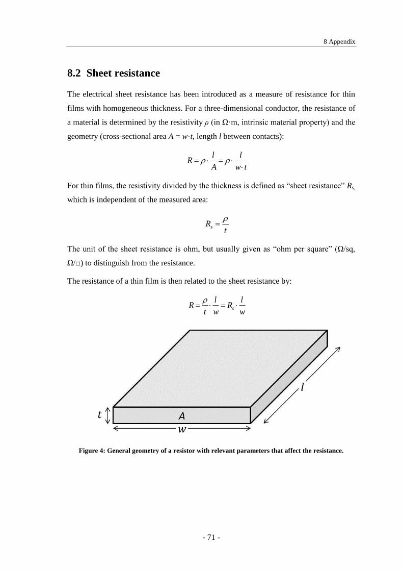
8 Appendix
- 71 -
8.2 Sheet resistance
The electrical sheet resistance has been introduced as a measure of resistance for thin
films with homogeneous thickness. For a three-dimensional conductor, the resistance of
a material is determined by the resistivity ρ (in Ω·m, intrinsic material property) and the
geometry (cross-sectional area A = w·t, length l between contacts):
For thin films, the resistivity divided by the thickness is defined as “sheet resistance” Rs,
which is independent of the measured area:
The unit of the sheet resistance is ohm, but usually given as “ohm per square” (Ω/sq,
Ω/) to distinguish from the resistance.
The resistance of a thin film is then related to the sheet resistance by:
Figure 4: General geometry of a resistor with relevant parameters that affect the resistance.
tw
l
A
lR
tRs
w
lR
w
l
tR s
8 Appendix
- 72 -
8.3 List of publications
(9) Spinning Hierarchical Gold Nanowire Microfibers by Shear Alignment and
Intermolecular Self-Assembly
B. Reiser, D. Gerstner, L. González-García, J. H. M. Maurer, I. Kanelidis, and
T. Kraus
ACS Nano, 2017, 11, 4934-4942
(8) Direct nanoimprinting of a colloidal self-organizing nanowire ink for flexi-
ble, transparent electronics
J. H. M. Maurer, L. González-García, I. K. Backes, B. Reiser, S. M. Schloss-
berg, and T. Kraus
Adv. Mater. Technol., 2017, 1700034
(7) Multivalent bonds in self-assembled bundles of ultrathin gold nanowires
B. Reiser, D. Gerstner, L. Gonzalez-Garcia, J. H. M. Maurer, I. Kanelidis, and
T. Kraus
Phys. Chem. Chem. Phys., 2016, 18, 27165-27169
(6) Ultrathin gold nanowires for transparent electronics: Soft sintering and
temperature stability
J. H. M. Maurer, L. González-García, B. Reiser, I. Kanelidis, and T. Kraus
Phys. Status Solidi A, 2016, 213, 2336–2340
(5) Templated Self-Assembly of Ultrathin Gold Nanowires by Nanoimprinting
for Transparent Flexible Electronics
J. H. M. Maurer, L. González-García, B. Reiser, I. Kanelidis, and T. Kraus
Nano Lett., 2016, 16, 2921-2925
(4) Gold nanorods with conjugated polymer ligands: sintering-free conductive
inks for printed electronics
B. Reiser, L. Gonzalez-Garcia, I. Kanelidis, J. H.M. Maurer, and T. Kraus
RSC Chem. Sci., 2016, 7, 4190-4196
(3) Ultrathin gold nanowires for transparent electronics: breaking barriers
L. González-García, J. H. M. Maurer, B. Reiser, I. Kanelidis and T. Kraus
Procedia Eng. 2016, 141, 152–156
(2) Sintering of ultrathin gold nanowires for transparent electronics
J. H. M. Maurer, L. González-García, B. Reiser, I. Kanelidis and T. Kraus
ACS Appl. Mater. Inter., 2015, 7, 7838-7842
(1) Genetically improved monolayer-forming tobacco mosaic viruses to gener-
ate nanostructured semiconducting bio/inorganic hybrids
P. Atanasova, N. Stitz, S. Sanctis, J. H. M. Maurer, R. C. Hoffmann, S. Eiben,
H. Jeske, J. J. Schneider and J. Bill
Langmuir, 2015, 31, 3897-3903
8 Appendix
- 73 -
8.4 Conference contributions
Oral contributions:
LOPEC 2016, Munich, Germany
Oral presentation: “Direct nanoimprint of metal nanowires for transparent electronics”
Apr 5-7, 2016
EMRS Fall Meeting 2015, Warsaw, Poland
Oral presentation: “Soft Sintering of Ultrathin Gold Nanowires for Transparent Elec-
tronics”
Sep 15-18, 2015, Materials Horizon best presentation award
57th Electronic Materials Conference, Ohio State University, Columbus, OH, USA
Oral presentation: “Ultrathin gold nanowires for transparent electronics: decreasing the
wire-wire junction resistance by annealing”
June 24-26, 2015
Poster contributions:
PhD Day 2016, Saarland University, Saarbrücken, Germany
Poster presentation: “Innovative ink concepts for transparent and printed electronics”
November 9, 2016
PhD Day 2014, Saarland University, Saarbrücken, Germany
Poster presentation: “Metal-Polymer Nanocomposites with structural control”
November 12, 2014
40th International Micro and Nano Engineering Conference (MNE), Swiss Tech
Convention Center, Lausanne, Switzerland
Poster presentation: “Aligned metal nanostructures by convective self-assembly using
pre-patterned transparent polymer”
September 22-26, 2014