Embed Size (px)
Citation preview
Gesellschaft für Mikroelektronik
The Society for Microelectronics
Annual Report
1998
Vienna, April 1999

Gesellschaft für Mikroelektronik
The Society for Microelectronics
Annual Report
1998
Gesellschaft für Mikroelektronikc/o Technische Universität Wien
Institut für Angewandte Elektronik und QuantenelektronikGußhausstraße 27-29/359, A-1040 Wien
Vienna, April 1999

Editor: Karl Riedling
Layout: Claudia BenedelaKarl Riedling
© 1999 Gesellschaft für Mikroelektronik (GMe)c/o Technische Universität WienInstitut für Angewandte Elektronik und QuantenelektronikGußhausstraße 27-29/359, A-1040 Wien
The Society for Microelectronics – Annual Report 1999 3
The Society for Microelectronics(GMe — Gesellschaft für Mikroelektronik)
E. Gornik, K. Riedling
Gesellschaft für Mikroelektronik,c/o Institut für Allgemeine Elektrotechnik und Elektronik, TU Wien
Gußhausstraße 27 – 29, A-1040 Wien
1. Goals of the Society for MicroelectronicsThe Society for Microelectronics (GMe) was founded in 1985 with the aim to “supportmicroelectronics technology and its applications” in Austria. The GMe defines its tasksas follows:
• Support of university-based “high-tech” research in the areas of microelectronics,semiconductor technology, sensors, and opto-electronics;
• Operation of research facilities;
• Support and consulting for industry, in particular, for small and medium enterprises,within the area of microelectronics.
The central task of the GMe is to provide an internationally competitive infra-structurein the area of microelectronics technology. The GMe allocates funds to maintain re-search projects in the fields of semiconductor technology, sensors, opto-electronics, andASIC design. Thus the infra-structure support generates a base for research projects thatare funded by other funding agencies.
2. Activities of the SocietyThe present focal point activities of the GMe are:
• Operation of university-based laboratories for microelectronics technology;
• Design of application specific integrated circuits (ASICs) —TMOe.
The GMe currently supports mainly the first focal point activity but also coordinates theAustria-wide activities of the TMOe program.
The main task of the GMe in the area of microelectronics technology is the operation ofthe cleanroom laboratories in Vienna and Linz. The GMe has coordinated the construc-tion of the Microstructure Center (MISZ — Mikrostrukturzentrum) in Vienna; the fundswere supplied by the Austrian Federal Ministry of Science and Research. The GMe nowfinances a significant part of the operation costs for the cleanroom laboratories in Vi-enna and Linz.
4 E. Gornik, K. Riedling
2.1 Microelectronics Technology — Cleanroom Vienna
The following university institutes receive support within this focal point activity:
• TU Wien:
− Institut für Festkörperelektronik
− Institut für Allgemeine Elektrotechnik und Elektronik
2.2 Microelectronics Technology — Cleanroom Linz
The following university institutes receive support within this focal point activity:
• Johannes Kepler Universität Linz:
− Institut für Halbleiterphysik
− Institut für Experimentalphysik
− Institut für Mikroelektronik
3. Other Activities of the SocietyOne of the declared tasks of the GMe is to provide information on current Austrian aca-demic activities in the field of microelectronics to industry, in particular to Austriansmall- and medium enterprises (SMEs). This will improve the transfer of “know-how”between Austrian universities and industry. As an example, the GMe supplied editorialarticles to an Austrian publishing house that targets its magazines on the managementand technical staff of Austrian industrial enterprises. The articles presented some ofthose projects supported by the GMe that had a direct impact on Austrian industry.
To enhance the distribution of the results of the research work done with GMe support,the GMe has put the contents of its previous annual reports — 1995 through 1997 — onits Web server; this will also happen for this report. Although we did not explicitly ad-vertise on a larger scale the existence of this server and its contents, it has apparentlybeen fairly well accepted by the international community. Access statistics show an av-erage access of 3 counts per day; however, an amazingly large percentage of these ac-cesses — close to 50 per cent — originates from net domains outside Austria. Aboutone quarter of the visitors of the GMe’s web site visited it more than once. The GMeWeb server is available under the URL:
http://www.iaee.tuwien.ac.at/gme/
Finally, the GMe prepared and carried out the biennial seminar “Aktuelle Entwicklungender Mikroelektronik” in Bad Hofgastein, Salzburg, which took place in March 1999.The predecessor of this seminar has first been held in 1977 in Großarl; since 1987, theGMe contributes financial support, and since 1993, the Society acts as its main organ-izer. The seminar presented thirteen invited lectures given by international experts, and25 oral and poster contributions which resulted from work supported by the GMe. Theprogram of this seminar is included in the appendix of this report. For the first time,greater emphasis was put into making the seminar more attractive to an industrial audi-ence, thus intending an enhanced knowledge transfer between universities and industry.
The Society for Microelectronics 5
4. The Annual Report for 1998 of the Society forMicroelectronics
The GMe is currently supporting the microelectronics technology activities of the clean-room laboratories in Vienna and Linz.
All projects described in this report were carried out in the cleanrooms in Vienna andLinz, respectively. They are not specific projects of the GMe but were funded by a vari-ety of other sources. They all have in common that they use the infra-structure providedby the GMe. It would therefore not have been possible to carry out these projects with-out the support by the GMe.

The Society for Microelectronics – Annual Report 1999 7
Contents
Microelectronics Technology — Cleanroom Vienna ........................ 9
G. Strasser: Cleanroom Vienna........................................................................ 11
T. Maier et al.: GaAs VCSELs with Dielectric Si3N4/SiO2 Mirrors ..................... 25
W. Schrenk et al.: GaAs/AlGaAs/InGaAs Bandgap Lasers — From DHLasers to VCSELs ........................................................................................ 29
P.O. Kellermann et al.: Wavelength Adjustable Surface Emitting SingleMode Laser Diodes with Contradirectional Surface Mode Coupling ............ 35
L. Hvozdara et al.: GaAs/AlGaAs Based Intersubband andInterminiband Mid-Infrared Emitters ............................................................. 41
J. Ulrich et al.: Far-Infrared Electroluminescence in Parabolic QuantumWells ............................................................................................................ 47
A. Lugstein et al.: Focused Ion Beam Technology – A New Approachfor the Sub 100 nm Microfabrication Regime ............................................... 51
C. Fürböck et al.: Internal Characterization of IGBTs Using theBackside Laserprobing Technique ............................................................... 57
R. Heer et al.: Enhanced Energy Resolution in Ballistic ElectronEmission Microscopy Through InAs Base Layers ........................................ 63
C. Rauch et al.: Onset of Scattering Induced Miniband Transport ................... 67
N. Finger et al.: Analysis of Single-Mode Grating Coupled TwinWaveguide Laser Structures ........................................................................ 71
Microelectronics Technology — Cleanroom Linz ........................... 75
G. Bauer et al.: Microstructure Research: Cleanroom Linz .............................. 77
C.G. Diskus et al.: A Ka-Band Detector Diode with High Sensitivity................. 93
M. Mühlberger et al.: Carbon Co-Doping of Si1-xGex:B Layers:Suppression of Transient Enhanced Diffusion ............................................. 99
N. Sandersfeld et al.: Modulation Doped Si/Si1-xGex-Field-EffectTransistors.................................................................................................. 103
C. Schelling et al.: Growth Instabilities in Si Homoepitaxy.............................. 107
J. Stangl et al.: Fast Growth Method for the Fabrication of ModulationDoped Si/SiGe Field Effect Transistors...................................................... 111
Y. Zhuang et al.: Si/SiGe Layers on Patterned Substrates for MODFETApplications ................................................................................................ 117
H. Seyringer et al.: Electron Beam Lithography of Nanostructures ................ 121
8 Contents
K. Wiesauer et al.: Fabrication of Semiconductor Nanostructures byScanning Force Microscopy ....................................................................... 127
S. Lanzerstorfer et al.: Light Generation by Er in Si Related Materials........... 131
G. Springholz et al.: Fabrication of Highly Efficient Mid-Infrared BraggMirrors from IV-VI Semiconductors ............................................................ 135
Th. Schwarzl et al.: CH4/H2 Plasma Etching of IV-VI Semiconductors ........... 139
W. Heiss et al.: ZnCdSe/ZnSe Quantum Wires by Epitaxy onPrepatterned GaAs Substrates .................................................................. 143
A. Bonanni et al.: Self-Assembling Mn-Based Nanostructures....................... 147
M. Pinczolits et al.: Molecular Beam Epitaxy Growth of 3D QuantumDot Crystals................................................................................................ 153
Appendix...................................................................................... 157
Program of the Seminar 'Aktuelle Entwicklungen der Mikroelektronik' ........... 159
The Society’s Managing Committee and Address.......................................... 163

The Society for Microelectronics – Annual Report 1999 9
MicroelectronicsTechnology —
Cleanroom Vienna

The Society for Microelectronics – Annual Report 1999 11
Cleanroom ViennaG. Strasser
Institut für Festkörperelektronik, Technische Universität Wien,Floragasse 7, A–1040 Vienna, Austria
We report on the main activities in the cleanroom of the MISZ (microstructure cen-ter). The cleanroom of the MISZ was opened 1993; during 1994, most of the equip-ment for the production of semiconductor devices was installed. Since 1995, state ofthe art growth of III–V compounds as well as the production of patterned masks usedin lithography is done on a regular basis. In spring 1998 state of the art Silicon proc-essing has been added as an additional material system. This activity is starting upand may need further support to mature. A short description of projects with a highcontent of technological input in our institute is given.
One of the main research areas of this institution is the preparation and characteriza-tion of III–V devices. Therefore the MISZ, namely the fke, maintains several col-laborations with national and international research institutions and companies byproviding them with epitaxial layers (III–V compounds). A second main researchtopic is the production of micron and sub-micron devices down to nanometer scale.Patterned masks for optical lithography are provided to different institutions.
1. IntroductionSince 1995, the cleanroom of the MISZ is running on a regular basis. Main researchareas are the state of the art growth of III-V compounds and the production of patternedmasks. Testing of the cleanroom quality and adjustment (laminar air flow, filters, cool-ing, humidity…) if necessary is done periodically.
The cleanroom contains all major components for semiconductor device processing(both on silicon and GaAs basis) and is equipped with a conventional photolithographyincluding a mask fabrication facility, e-beam lithography for nm structures, evaporationchambers, an ion milling chamber, and a plasma etching and plasma deposition chamberin master-slave configuration.
In 1998, the following additional equipment was installed :
• an RF sputtering chamber for deposition of metals and dielectric materials;
• a focussed ion beam (“FIB”) writer;
• an additional wet bench was installed for chemical processes.
The RF sputtering chamber is mainly used for the deposition of dielectric mirrors, whichare necessary for the fabrication of surface emitting lasers.
The FIB writer is currently the ultimate tool in nanofabrication technology. This ma-chine is basically a scanning ion microscope (similar to a scanning electron microscope)with the additional abilities to deposit arbitrary metal structures in the deep sub-µm re-gime and to etch holes in predefined deep sub-µm geometries.
In the following chapters, the main research activities making use of the cleanroom it-self or using samples grown, structured and tested in the MISZ are described. These

12 G. Strasser
activities are not the only projects running in the MISZ, but are intended to show a rep-resentative overview on basic research as well as applied projects using the existingequipment. For a more general overview the added project information, specially theattached publication list from the last year, may give some insides on the broad range ofactivities.

Cleanroom Vienna 13
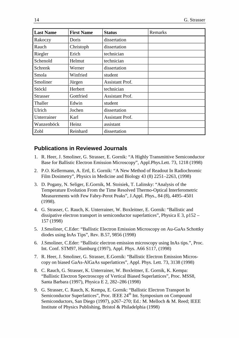
Project Information
Project ManagerDr. Gottfried STRASSER
Institut für Festkörperelektronik, Technische Universität Wien
Project Group
Last Name First Name Status Remarks
Bertagnolli Emmerich Full Prof.
Boxleitner Winfried Post Doc
Bratschitsch Rudolf dissertation
Finger Norman dissertation
Fuchshuber Michael student
Fürböck Christoph dissertation
Gianordoli Stefan dissertation
Gornik Erich Full Prof.
Haider Manfred student
Heer Rudolf dissertation
Hirner Heimo student
Hobler Gerhard Assistant Prof.
Hoffmann Rainer student
Hvozdara Lubos dissertation
Kast Michael student
Kellermann Peer Oliver dissertation
Kersting Roland Post Doc
Kröll Peter technician
Lampacher Peter student
Langmann Gottfried technician
Litzenberger Martin dissertation
Lugstein Alois assistant
Maier Thomas dissertation
Pacher Christoph dissertation
Patz Sybille student
Ploner Guido dissertation
Pogany Dionyz guest scientist
Prinzinger Johannes technician
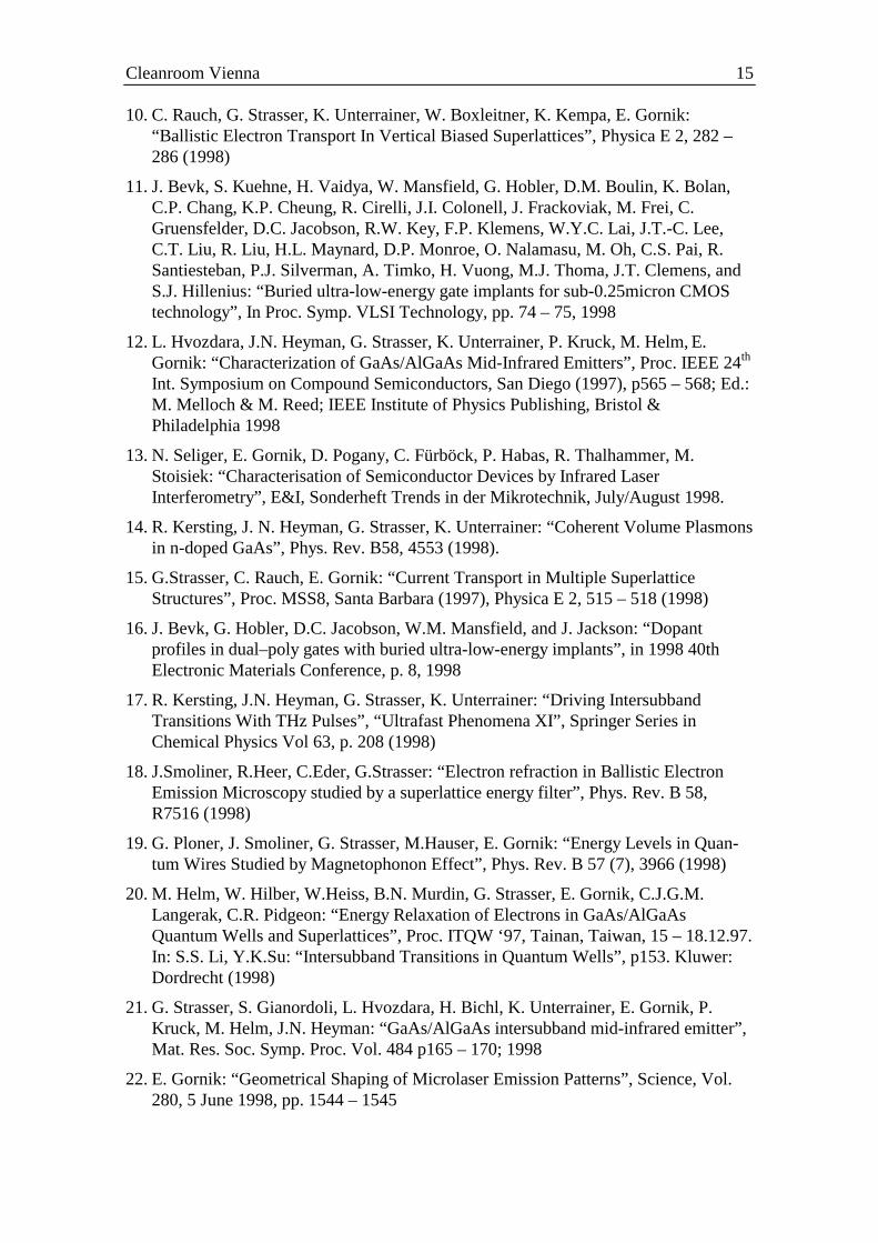
14 G. Strasser
Last Name First Name Status Remarks
Rakoczy Doris dissertation
Rauch Christoph dissertation
Riegler Erich technician
Schenold Helmut technician
Schrenk Werner dissertation
Smola Winfried student
Smoliner Jürgen Assistant Prof.
Stöckl Herbert technician
Strasser Gottfried Assistant Prof.
Thaller Edwin student
Ulrich Jochen dissertation
Unterrainer Karl Assistant Prof.
Wanzenböck Heinz assistant
Zobl Reinhard dissertation
Publications in Reviewed Journals1. R. Heer, J. Smoliner, G. Strasser, E. Gornik: “A Highly Transmittive Semiconductor
Base for Ballistic Electron Emission Microscopy”, Appl.Phys.Lett. 73, 1218 (1998)
2. P.O. Kellermann, A. Ertl, E. Gornik: “A New Method of Readout In RadiochromicFilm Dosimetry”, Physics in Medicine and Biology 43 (8) 2251–2263, (1998)
3. D. Pogany, N. Seliger, E.Gornik, M. Stoisiek, T. Lalinsky: “Analysis of theTemperature Evolution From the Time Resolved Thermo-Optical InterferometricMeasurements with Few Fabry-Perot Peaks”, J.Appl. Phys., 84 (8), 4495–4501(1998).
4. G. Strasser, C. Rauch, K. Unterrainer, W. Boxleitner, E. Gornik: “Ballistic anddissipative electron transport in semiconductor superlattices”, Physica E 3, p152 –157 (1998)
5. J.Smoliner, C.Eder: “Ballistic Electron Emission Microscopy on Au-GaAs Schottkydiodes using InAs Tips”, Rev. B.57, 9856 (1998)
6. J.Smoliner, C.Eder: “Ballistic electron emission microscopy using InAs tips.”, Proc.Int. Conf. STM97, Hamburg (1997), Appl. Phys. A66 S117, (1998)
7. R. Heer, J. Smoliner, G. Strasser, E.Gornik: “Ballistic Electron Emission Micros-copy on biased GaAs-AlGaAs superlattices”, Appl. Phys. Lett. 73, 3138 (1998)
8. C. Rauch, G. Strasser, K. Unterrainer, W. Boxleitner, E. Gornik, K. Kempa:“Ballistic Electron Spectroscopy of Vertical Biased Superlattices”, Proc. MSS8,Santa Barbara (1997), Physica E 2, 282–286 (1998)
9. G. Strasser, C. Rauch, K. Kempa, E. Gornik: “Ballistic Electron Transport InSemiconductor Superlattices”, Proc. IEEE 24th Int. Symposium on CompoundSemiconductors, San Diego (1997), p267–270; Ed.: M. Melloch & M. Reed; IEEEInstitute of Physics Publishing, Bristol & Philadelphia (1998)
Cleanroom Vienna 15
10. C. Rauch, G. Strasser, K. Unterrainer, W. Boxleitner, K. Kempa, E. Gornik:“Ballistic Electron Transport In Vertical Biased Superlattices”, Physica E 2, 282 –286 (1998)
11. J. Bevk, S. Kuehne, H. Vaidya, W. Mansfield, G. Hobler, D.M. Boulin, K. Bolan,C.P. Chang, K.P. Cheung, R. Cirelli, J.I. Colonell, J. Frackoviak, M. Frei, C.Gruensfelder, D.C. Jacobson, R.W. Key, F.P. Klemens, W.Y.C. Lai, J.T.-C. Lee,C.T. Liu, R. Liu, H.L. Maynard, D.P. Monroe, O. Nalamasu, M. Oh, C.S. Pai, R.Santiesteban, P.J. Silverman, A. Timko, H. Vuong, M.J. Thoma, J.T. Clemens, andS.J. Hillenius: “Buried ultra-low-energy gate implants for sub-0.25micron CMOStechnology”, In Proc. Symp. VLSI Technology, pp. 74 – 75, 1998
12. L. Hvozdara, J.N. Heyman, G. Strasser, K. Unterrainer, P. Kruck, M. Helm, E.Gornik: “Characterization of GaAs/AlGaAs Mid-Infrared Emitters”, Proc. IEEE 24th
Int. Symposium on Compound Semiconductors, San Diego (1997), p565 – 568; Ed.:M. Melloch & M. Reed; IEEE Institute of Physics Publishing, Bristol &Philadelphia 1998
13. N. Seliger, E. Gornik, D. Pogany, C. Fürböck, P. Habas, R. Thalhammer, M.Stoisiek: “Characterisation of Semiconductor Devices by Infrared LaserInterferometry”, E&I, Sonderheft Trends in der Mikrotechnik, July/August 1998.
14. R. Kersting, J. N. Heyman, G. Strasser, K. Unterrainer: “Coherent Volume Plasmonsin n-doped GaAs”, Phys. Rev. B58, 4553 (1998).
15. G.Strasser, C. Rauch, E. Gornik: “Current Transport in Multiple SuperlatticeStructures”, Proc. MSS8, Santa Barbara (1997), Physica E 2, 515 – 518 (1998)
16. J. Bevk, G. Hobler, D.C. Jacobson, W.M. Mansfield, and J. Jackson: “Dopantprofiles in dual–poly gates with buried ultra-low-energy implants”, in 1998 40thElectronic Materials Conference, p. 8, 1998
17. R. Kersting, J.N. Heyman, G. Strasser, K. Unterrainer: “Driving IntersubbandTransitions With THz Pulses”, “Ultrafast Phenomena XI”, Springer Series inChemical Physics Vol 63, p. 208 (1998)
18. J.Smoliner, R.Heer, C.Eder, G.Strasser: “Electron refraction in Ballistic ElectronEmission Microscopy studied by a superlattice energy filter”, Phys. Rev. B 58,R7516 (1998)
19. G. Ploner, J. Smoliner, G. Strasser, M.Hauser, E. Gornik: “Energy Levels in Quan-tum Wires Studied by Magnetophonon Effect”, Phys. Rev. B 57 (7), 3966 (1998)
20. M. Helm, W. Hilber, W.Heiss, B.N. Murdin, G. Strasser, E. Gornik, C.J.G.M.Langerak, C.R. Pidgeon: “Energy Relaxation of Electrons in GaAs/AlGaAsQuantum Wells and Superlattices”, Proc. ITQW ‘97, Tainan, Taiwan, 15 – 18.12.97.In: S.S. Li, Y.K.Su: “Intersubband Transitions in Quantum Wells”, p153. Kluwer:Dordrecht (1998)
21. G. Strasser, S. Gianordoli, L. Hvozdara, H. Bichl, K. Unterrainer, E. Gornik, P.Kruck, M. Helm, J.N. Heyman: “GaAs/AlGaAs intersubband mid-infrared emitter”,Mat. Res. Soc. Symp. Proc. Vol. 484 p165 – 170; 1998
22. E. Gornik: “Geometrical Shaping of Microlaser Emission Patterns”, Science, Vol.280, 5 June 1998, pp. 1544 – 1545
16 G. Strasser
23. R. Thalhammer, C. Fürböck, N. Seliger, G. Deboy, E. Gornik, G. Wachutka:“Internal Characterization of IGBTs Using the Backside Laser Probing Technique –Interpretation of Measurement by Numerical Simulation”, Proc. of ISPSD´98, pp.199 – 202.
24. B.N. Murdin, N. Nasser, C.J.G.M. Langerak, W.Heiss, M. Helm, G. Strasser,E. Gornik, S.–C. Lee, I. Galbraith, C.R. Pidgeon: “Intersubband dynamics below theoptical energy for single and coupled quantum well systems”, Phys. stat. sol. (b) 204,208 (1997)
25. L. Pelaz, G.H. Gilmer, M. Jaraiz, S.B. Herner, H.–J. Gossmann, D.J. Eaglesham, G.Hobler, C.S. Rafferty, and J. Barbolla: “Modeling of the ion mass effect on transientenhanced diffusion: deviation from the “+1” model”, Appl. Phys. Lett., 73(10), 1421– 1423, 1998
26. C. Eder, J. Smoliner, R. Heer, G. Strasser, E. Gornik: “Probing of SuperlatticeMinibands by Ballistic Electron Emission Microscopy”, Proc. MSS8, Santa Barbara(1997), Physica E 2, 850 – 853 (1998)
27. P. Kruck, G.Strasser, M. Helm, L. Hvozdara, E. Gornik: “Quantum CascadeElectroluminescence in GaAs/AlGaAs Structures”, Proc. MSS8, Santa Barbara(1997), Physica E 2, 449 – 452 (1998)
28. P. Kruck, M. Helm, G. Strasser, L. Hvozdara, E. Gornik: “Quantum CascadeElectroluminescence in the GaAs/AlGaAs Material System”, In: S. S. Li, Y. K. Su:“Intersubband Transitions in Quantum Wells”, p17. Kluwer: Dordrecht (1998)
29. D. Pogany, N. Seliger, T. Lalinsky, J. Kuzmík, P. Habas, P. Hrkút and E. Gornik:“Study of Thermal Effects in GaAs Micromachined Power Sensor Microsystems byan Optical Interferometer Technique”, Microelectronics Journal, vol.29, pp.191 –198, (1998).
30. H.-J. Gossmann, C.S. Rafferty, G. Hobler, H.-H. Vuong, and D.C. Jacobson:“Suppression of reverse short channel effect by a buried carbon layer”, In 1998IEDM Techn. Dig., pp. 725 – 728. IEEE, Piscataway, 1998
31. E. Burian, D. Pogany, T. Lalinsky, N. Seliger and E. Gornik: “Thermal Simulationand Characterization of GaAs Micromachined Power Sensor Microsystems”,Sensors and Actuators: A.Physical, Vol.68, p.372 – 377 (1998).
32. T. Lalinsky, I. Hotovy, S. Hascik, Z. Mozolova, J. Kuzmik, D. Pogany: “Thin FilmResistance Temperature Sensors on GaAs”, In Proc. ASDAM’98, Smolenice,Slovakia, October 5 – 7, (1998) pp. 243 – 246, Eds. J. Breza, D. Donoval, V.Drobny, F.Uherek.
33. J.N. Heyman, R. Kersting, G. Strasser, K.D. Maranowski, A.C. Gossard, K.Unterrainer: “THz Time-Domain Spectroscopy of Interssubband Plasmons”, in“Intersubband Transitions in Quantum Wells: Physics and Devices” Eds. S. S. Liand Y. K. Su, Kluwer, Dordrecht, 1998
34. J.N. Heyman, R. Kersting, K. Unterrainer: “Time-Domain Measurement ofIntersubband Oscillations in a Quantum Well”, Appl. Phys. Lett., 72, 644 (1998).
35. Rauch, G. Strasser, K. Unterrainer, W. Boxleitner, E. Gornik, A. Wacker:“Transition between coherent and incoherent electron transport in GaAs/GaAlAssuperlattices”, Phys. Rev. Lett. 81 (16), 3495 (1998)
Cleanroom Vienna 17
36. E. Gornik, C. Rauch, G. Strasser: “Transition From Coherent to IncoherentSuperlattice Transport”, Proc. 6th International Symposium on Nanostructures:Physics and Technology, St. Petersburg, Russia, 50 (1998)
37. C. Messner, H. Kostner, R.A. Höpfel, K. Unterrainer: “Ultrafast THz TransmissionSpectroscopy on Proton Bombarded In P”, In: Trends in Optics and Photonics(TOPS), Vol 18 – Radiative Processes and Dephasing in Semiconductors, Ed. D.Citrin (Optical Society of America, 1998).
38. R. Thalhammer, C. Fürböck, N. Seliger, E. Gornik, G. Wachutka: “Validation andcalibration of Electrothermal Device Models Using Infrared Laser ProbingTechniques”, published in MSM’ 98
39. R. von Criegern, F. Jahnel, R. Lange–Gieseler, P. Pearson, G. Hobler, and A.Simionescu: “Verification of lateral secondary ion mass spectrometry as a methodfor measuring lateral dopant dose distributions in microelectronics test structures”, J.Vac. Sci. Technol., B 16(1), 386 – 393, 1998
Submitted papers :
1. G.Ploner, H.Hirner, T.Maier, G.Strasser, J.Smoliner and E.Gornik: “A device layoutfor tunneling spectroscopy of barrier separated electron systems with tunabledimensionality”, submitted to Appl. Phys. Lett.
2. R.Heer, J.Smoliner, G.Strasser E.Gornik: “A highly transmittive semiconductor basefor Ballistic Electron Emission Microscopy”, Proc. SXM3 Basel (1998), submitted
3. O. Csabay, K. Gmucová, I. Thurzo, E. Gornik, G. Strasser, L. Hvozdara, L.Harmatha: “An Experimental Study of AlGaAs/GaAs Heterostructures Using anAdvanced Transient Charge Processor”, submitted to SST
4. C. Fürböck, N. Seliger, D. Pogany, M. Litzenberger, E. Gornik, M. Stecher, H.Goßner, W. Werner: “Backside Laserprober Characterization of Thermal Effectsduring High Current Stress in Smart Power ESD Protection Devices”, Proc. IEDM1998, San Francisco, Dec 6–9th, 1998; accepted for publication
5. J. Smoliner, R. Heer, G. Strasser: “Biased GaAs–AlGaAs superlattices employed asenergy filter for Ballistic Electron Emission Microscopy”, Proc. SXM3 Basel(1998), submitted
6. G. Hobler, J. Bevk, and A. Agarwal: “Channeling of low-energy implanted ionsthrough the poly–Si gate”, IEEE Electron Dev. Lett. (submitted for publication).
7. N. Seliger, E. Gornik, D. Pogany, C. Fürböck, P. Habas, R. Thalhammer, M.Stoisiek: “Characterisation of Semiconductor Devices by Infrared LaserInterferometry”, to be published in E&I, Sonderheft Trends in der Mikrotechnik,July/August 1998.
8. Rauch, M. Kast, G. Strasser, K. Unterrainer, A. Wacker, S. Bose, E. Gornik:“Coherence Length of Ballistically Injected Hot Electrons in GaAs/AlGaAsSuperlattices”, Proc. 24th International Conference on the Physics ofSemiconductors, Jerusalem, Israel, 3.–7.8.1998
9. R. Kersting, J.N. Heyman, G. Strasser, K. Unterrainer: “Coherent Plasma Oscilla-tions of Extrinsic Electrons”, submitted to “Ultrafast Phenomena ‘98”, (1998). Inpress.
18 G. Strasser
10. G. Hobler, L. Pelaz, and C.S. Rafferty: “Continuum treatment of spatial correlationin damage annealing”, Nucl. Instr. Meth. B (accepted for publication).
11. M. Helm, W. Hilber, G. Strasser, R. De Meester, F.M. Peeters, A. Wacker:“Continuum Wannier–Stark ladders strongly interacting by Zener resonances insemiconductor superlattices”, submitted to PRL, 6.11.98
12. E. Gornik, C.M. Engelhardt and G. Abstreiter: “Cyclotron Resonance of N–GaAsSingle Quantum Wells – Localization and Scattering Effects”, submitted to WorldScientific
13. C.M. Engelhardt, E. Gornik, G. Böhm: “Cyclotron Resonance of n–GaAs SingleQuantum Wells – Localization, Scattering Processes, Electron Electron Interactionand Quantum Mechanical Oscillator Strength”, submitted to World Scientific
14. C. Eder, J. Smoliner, R. Heer, G. Strasser, E. Gornik: “Direct Observation ofSuperlattice Minibands by Ballistic Electron Emission Microscopy”, Proc. 9th Int.Conf. STM 97, Hamburg (1997)
15. G. Hobler, L. Pelaz, and C.S. Rafferty: “Dose, energy, and ion species dependenceof the effective plusfactor for transient enhanced diffusion”, In Process Physics andModeling in Semiconductor Technology (G.R. Srinivasan, C.S. Murthy, and S.T.Dunham, editors). The Electrochem. Soc., Pennington, 1999 (submitted forpublication).
16. R. Kersting, J.N. Heyman, R. Hoffmann, G. Strasser, K.D. Maranowski, A.C.Gossard, K. Unterrainer: “Driving a Harmonic Quantum Oscillator With Few-CycleTHz Pulses”, Proc. International Quantum Electronics Conference 98, SanFrancisco, USA, 1. – 5. 5. 1998. Submitted and accepted.
17. J.Smoliner, R.Heer, C.Eder, G.Strasser: “Electron Refraction in Ballistic ElectronEmission Microscopy Studied by a Superlattice Energy Filter”, Accepted at Phys.Rev. B (1998)
18. K. Unterrainer, R. Kersting, G. Strasser, J.N. Heyman, K.D. Maranowski, A.C.Gossard: “Few-Cycle THz Spectroscopy of Nanostructures”, Proc. 24th InternationalConference on the Physics of Semiconductors, Jerusalem, Israel, 3. –7.8.1998.
19. G. Strasser, S. Gianordoli, L. Hvozdara, K. Unterrainer, E. Gornik, P. Kruck, M.Helm: “GaAs/AlGaAs Quantum Cascade Intersubband Emitter”, Proc. 24thInternational Conference on the Physics of Semiconductors, Jerusalem, Israel, 3. –7.8.1998
20. G. Strasser, L. Hvozdara, S. Gianordoli, K. Unterrainer, E. Gornik, P. Kruck, M.Helm: “GaAs/AlGaAs Quantum Cascade Intersubband and Interminiband Emitter”,Proc. 10th International Conference on Molecular Beam Epitaxy, Cannes, France,31.8. – 4.9.1998, accepted at the Journal of Crystal Growth
21. O. Gauthier–Lafaye, F.H. Julien, S. Cabaret, J.-M. Lourtioz, G. Strasser, E. Gornik,M. Helm, P. Bois: “High-power GaAs/AlGaAs Quantum Fountain Laser emitting at14.5 µm with 2.5% tunability”, to be submitted to Appl. Phys. Lett.
22. K. Kempa, P. Bakshi, C. Du, G. Feng, A. Scoropsky, E. Gornik, G. Strasser, K.Unterrainer, C. Rauch: “Intersubband Scattering Rates, Population Inversion andStimulated Emission of THz Plasmons in Bounded Quantum Systems”, Proc. 24th
Cleanroom Vienna 19
International Conference on the Physics of Semiconductors, Jerusalem, Israel, 3. –7.8.1998
23. N.E. Hecker, R.A. Höpfel, N. Sawaki, T. Maier, G. Strasser: “Large Enhancement inQuantum Well Luminescence Intensity Due to Surface Plasmons Excited on aMetallic Grating”, Proc. 24th International Conference on the Physics ofSemiconductors, Jerusalem, Israel, 3. – 7.8.1998
24. G. Ploner, J. Smoliner, M. Hauser, G. Strasser, E. Gornik: “MagnetophononResonances as a Tool for the Characterization of Quantum Wire Systems”, to bepublished
25. D. Stifter, W. Heiß, A. Bonanni, G. Prechtl, M. Schmid, K. Hingerl, H. Seyringer,H. Sitter, J. Liu, E. Gornik, L. Tóth and Á Barna: “Molecular Beam Epitaxy ofZnCdSe/ZnSe Wires on Patterned Substrates”, submitted to APL
26. Rauch, G. Strasser, M. Kast, E. Gornik: “Mean Free Path of Ballistic Electrons inGaAs/AlGaAs Superlattices”, to be published in Superlattices and Microstructures;Proc. ICMMS ‘98
27. R. Hoffmann, R. Kersting, J.N. Heyman, G. Strasser, K. Unterrainer, K.D.Maranowski, A.C. Gossard: “Optically Driven Parabolic Quantum Wells as Few–Cycle THz Emitters”, Proc. of ICMMS 1998
28. W Fischler, R. Bratschitsch, R.A. Höpfel, G. Strasser, K. Unterrainer: “Oscillatoryelectron transport in GaAs/AlGaAs Superlattices”, Proc. European QuantumElectronics Conference 98, Glasgow, Scotland, 14. – 18. 9. 1998
29. B.N. Murdin, A.R. Hollingworth, M. Kamal–Saadi, R.T. Kotitschke, C.M. Ciesla,C.R. Pidgeon, P.C. Findlay, H.A. Pellemans, C.J.G.M. Langerak, A.C. Rowe, R.A.Stradling and E. Gornik: “Suppression of LO phonon scattering in ‘quasi’ quantumdots”, submitted to PRL
30. R. Heer, J. Smoliner, G. Strasser, E. Gornik: “Temperature Dependent BEEMStudies on InAs/GaAs Heterostructures”, Proc. 24th International Conference on thePhysics of Semiconductors, Jerusalem, Israel, 3. – 7.8.1998
31. J.Smoliner, R.Heer, G.Strasser: “Temperature dependent studies of InAs base layersfor Ballistic Electron Emission Microscopy”, submitted to Phys. Rev. B (1998)
32. R. Zobl, M. Fuchshuber, G. Strasser, K. Unterrainer, E. Gornik, K.D. Maranowski,A.C. Gossard: “THz Emission from Parabolically Graded Quantum Wells in TiltedMagnetic Fields”, Proc. of the 6th IEEE Int. Conf. on Terahertz Electronics, Leeds,UK, 3. – 4.9.1998.
33. J.N. Heyman, R. Kersting, G. Strasser, K. Unterrainer, K. Maranowski, A.C.Gossard: “THz Time–Domain Spectroscopy of Intersubband Transitions”, Proc.24th International Conference on the Physics of Semiconductors, Jerusalem, Israel,3. – 7.8.1998.
34. R. Kersting, J.N. Heyman, G. Strasser, K. Unterrainer: “THz Time–DomainSpectroscopy of Intersubband Transitions”, Proc. International Quantum ElectronicsConference 98, San Francisco, USA, 1. – 5. 5. 1998
35. K. Kempa, P. Bakshi, C. Du, G. Feng, A. Scoropsky, G. Strasser, C. Rauch, K.Unterrainer, E. Gornik: “Towards the generation of coherent plasmons”, to besubmitted to Phys.Rev.B
20 G. Strasser
36. Wacker, S. Bose, C. Rauch, G. Strasser, E. Gornik: “Transmission throughSuperlattices with Interface Roughness”, to be published in Superlattices andMicrostructures; Proc. ICMMS ‘98
37. R. Kersting, J.N. Heyman, G. Strasser, K. Unterrainer: “Ultrafast Dynamics ofCoherent Plasmons in n-doped GaAs”, Proc. “European Quantum ElectronicsConference, EQEC 1998”, QMC2 (1998)
38. J.N. Heyman, R. Kersting, G. Strasser, K. Unterrainer, K. Maranowski, A.C.Gossard: “Ultrafast THz Spectroscopy of Intersubband Transitions in QuantumWells”, Submitted to Journal of Applied Physics
39. H.–H. Vuong, Y.–H. Xie, M.R. Frei, G. Hobler, L. Pelaz, and C.S. Rafferty: “Use oftransient enhanced diffusion to tailor boron out-diffusion”, IEEE Trans. ElectronDev. (submitted for publication).
40. R. Thalhammer, C. Fürböck, N. Seliger, E. Gornik, G. Wachutka: “Validation andCalibration of Electrothermal Device Models Using Infrared Laser ProbingTechniques”, published in MSM´98.
41. M. Mastrapasqua, G. Hobler, and E. Sangiorgi: “Vertically integrated SRAM”, InFuture Trends in Microelectronics: Off the Beaten Path, 1999 (accepted forpublication).
Presentations1. E. Gornik: “Advanced Semiconductor Devices And Microsystems”, Smolenice,
Slovakia, 5.–7.10.1998
2. E. Gornik: “Die Rolle der Universitäten als Wissensspender und Kooperations-partner”, Alpbacher Technologiegespräche 1998, Arbeitskreis: “EuropäischesRahmenprogramm und Nationale Technologiepolitik: Katalysator oderSteuerungsinstrument”
3. E. Gornik, J. Smoliner, R. Heer:”New Phenomenon in Mesoscopic Structures”(NPMS’98), 7. – 11.12.1998, Kauai, Hawai
4. E. Gornik: Chairman: “Magnetic Thin Films”, 14th International Vacuum Congress,31.8. – 4.9.1998, International Convention Centre, Birmingham, U.K.
5. E. Gornik: “Emission Direction Modulation of Diode Lasers”, European Conferenceon Lasers and Electro Optics/European Quantum Electronics Conference ‘98, SECCGlasgow, 13. – 18.09.1998, Glasgow, Scotland
6. R. Kersting, J.N. Heyman, G. Strasser, and K. Unterrainer: “Ultrafast dynamics ofcoherent plasmons in n-doped GaAs”, “European Quantum Electronics Conference”,14.09.– 18.09.1998, Glasgow, U.K.
7. R. Kersting, R. Bratschitsch, J.N. Heyman, G. Strasser, K. Unterrainer: “THzgeneration and spectroscopy”, “THz ‘98”, 03.09.– 04.09.1998, Leeds, U.K.
8. R. Kersting, J.N. Heyman, G. Strasser, and K. Unterrainer: “Driving intersubbandtransitions with few–cycle THz pulses”, “Ultrafast Phenomena ‘98”, 12. – 17. 07.1998, Garmisch–Partenkirchen, Germany
Cleanroom Vienna 21
9. J.N. Heyman, R. Kersting, K. Unterrainer, G. Strasser, E. Gornik: “Time–domainmeasurements of intersubband oscillations”, Workshop on “Radiative Processes andDephasing in Semiconductors”, 2. – 4.2.1998, Coueur d´Alene, Idaho, USA
10. C. Messner, H. Kostner, R.A. Höpfel, K. Unterrainer: “Ultrafast THz transmissionspectroscopy on proton bombarded InP”, Workshop on “Radiative Processes andDephasing in Semiconductors”, 2. – 4.2.1998, Coueur d´Alene, Idaho, USA
11. R. Kersting, J.N. Heyman, R. Hoffmann, G. Strasser, K.D. Maranowski, A.C.Gossard and K. Unterrainer: “Driving a harmonic quantum oscillator with few–cycleThz pulses”, International Qunatum Electronics Confernce, San Francisco, USA,1. – 5. 5. 1998
12. G. Strasser, C. Rauch, K. Unterrainer, W. Boxleitner, K. Kempa, E. Gornik:“Ballistic and dissipative electron transport in semiconductor superlattices”, Int.Winterschool on new developments in Solid State Physics; 23 – 27.2.98,Mauterndorf, Austria
13. K. Kempa, P. Bakshi, A. Scorupsky, G. Strasser, C. Rauch, K. Unterrainer, E.Gornik: “Search for plasma instability driven coherent emission in a quantum wellstructure”, APS March Meeting 1998, Los Angeles, USA
14. G. Strasser, S. Gianordoli, L. Hvozdara, K. Unterrainer, E. Gornik: “GaAs/AlGaAsQuantum Cascade Emitter”, 40th Electronic Materials Conference, Charlottesville,June 24 – 26.1998
15. C. Rauch, G. Strasser, E. Gornik: “Ballistic Electron Spectroscopy of semiconductorquantum devices”, 40th Electronic Materials Conference, Charlottesville 1998
16. J.N. Heyman, R. Kersting, G. Strasser, K. Unterrainer, K. Maranowski, A.C.Gossard: “THz Time–Domain Spectroscopy of Intersubband Transitions”, 24thInternational Conference on the Physics of Semiconductors, Jerusalem, Israel, 3.–7.8.1998.
17. K. Unterrainer, R. Kersting, G. Strasser, J.N. Heyman, K.D. Maranowski, A.C.Gossard: “Few-Cycle THz Spectroscopy of Nanostructures”, 24th InternationalConference on the Physics of Semiconductors, Jerusalem, Israel, 3. – 7.8.1998.
18. G. Strasser, S. Gianordoli, L. Hvozdara, K. Unterrainer, E. Gornik, P. Kruck, M.Helm: “GaAs/AlGaAs Quantum Cascade Intersubband Emitter”, ICPS-24,Jerusalem 1998
19. R. Heer, J. Smoliner, G. Strasser, E. Gornik: “Temperature Dependent BEEMStudies on InAs/GaAs Heterostructures”, ICPS-24, Jerusalem 1998
20. C. Rauch, G. Strasser, A. Wacker, K. Unterrainer, W. Boxleitner, E. Gornik: “MeanFree Path of Ballistic Electrons in GaAs/AlGaAs superlattices”, ICMMS ‘98
21. G. Strasser, S. Gianordoli, L. Hvozdara, K. Unterrainer, E. Gornik, P. Kruck, M.Helm: “GaAs/AlGaAs Quantum Cascade Intersubband and Interminiband Emitter”,MBE-X, Cannes, Aug. 31 – Sep. 4, 1998
22. R. Heer, C. Eder, J. Smoliner, G. Strasser, E. Gornik, “Low temperature BEEMstudies on InAs/GaAs Heterostructures”, Int. Winterschool on new developments inSolid State Physics; 23 – 27.2.98, Mauterndorf, Austria
22 G. Strasser
23. W. Hilber, M. Helm, G. Strasser; “Simultaneous observation of a Wannier Starkladder and negative differential resistance in a doped superlattice”; Int. Winterschoolon new developments in Solid State Physics; 23 – 27.2.98, Mauterndorf, Austria
24. L. Hvozdara, G. Strasser, S. Gianordoli, K. Unterrainer, P. Kruck, M. Helm, E.Gornik: “Growth and characterization of a GaAs/AlGaAs mid-infrared emitter”, Int.Winterschool on new developments in Solid State Physics; 23 – 27.2.98,Mauterndorf, Austria
25. C. Fürböck, N. Seliger, D. Pogany, M. Litzenberger, E. Gornik, M. Stecher, H.Goßner, W. Werner, “Backside Laserprober Characterization of Thermal Effectsduring High Current Stress in Smart Power ESD Protection Devices”, IEDM`98,San Francisco, USA, December 6 – 9, 1998.
26. R. Thalhammer, C. Fürböck, N. Seliger, E. Gornik, G. Wachutka, “Validation andcalibration of Electrothermal Device Models Using Infrared Laser ProbingTechniques”, MSM`98, Santa Clara, USA, April 6 – 8, 1998.
27. R. Thalhammer, C. Fürböck, N. Seliger, G. Deboy, E. Gornik, G. Wachutka:“Internal characterization of IGBTs using the backside laser probing technique –Interpretation of measurement by numerical simulation”, ISPSD`98, Kyoto, Japan,June 3 – 6, 1998.
28. R. Zobl, M. Fuchshuber, G. Strasser, K. Unterrainer, E. Gornik, K.D. Maranowski,A.C. Gossard: “THz Emission from Parabolically Graded Quantum Wells in TiltedMagnetic Fields”, 6th IEEE Int. Conf. on Terahertz Electronics, Leeds, UK, 3. –4.9.1998.
29. T.Lalinsky, I.Hotovy, S.Hascik, Z.Mozolova, J.Kuzmik, D.Pogany: “Thin filmresistance temperature sensors on GaAs”, in Proc. ASDAM’98, Smolenice,Slovakia, October 5–7, (1998) p.243–246, Eds. J. Breza, D. Donoval, V. Drobny,F.Uherek.
30. D.Pogany, N.Seliger, E.Gornik, T.Lalinsky, M.Stoisiek: “Thermal investigation ofthin film semiconductor devices by optical interferometry”, Int Workshop onDiagnostics of Solid State Surfaces and Interfaces, June 24 – 25, 1998, p.18,Bratislava, Slovakia, invited talk.
Doctor’s Theses1. N. Seliger, “Characterization of Semiconductor Devices by Laser Interferometry”,
TU Wien, 1998
2. Ch. Rauch: “Ballistic Electron Spectroscopy of Semiconductor Heterostructures”,TU Wien, 1998
Cooperations1. Universität Graz, Institut für Experimentalphysik, Prof. F. Aussenegg
2. Univ. Innsbruck, Inst. f. Experimentalphysik, Mag. Fischler, Dr. J. Schmiedmayer
3. Univ. Linz, Institut für Halbleiterphysik, ao. Prof. M. Helm
4. AMS–Unterpremstätten, Dr. F. Noll
Cleanroom Vienna 23
5. Siemens AG Villach/München: Dr. Prybil, Dr. Stecher, Dr. Kerber, Dr. Werner, Dr.B. Borchert , Dr. L. Korte, Prof. E. Wolfgang, Dr.M. Stoisiek, Dr. G. Deboy, Dr. G.Sölkner; Dr. S. Görlich Österreich/Deutschland
6. Plansee AG, Reutte, Dr. Willhartitz
7. Walter Schottky Institut, TU–München, Dr. W. Wegscheidler, Deutschland
8. TU München, Lehrstuhl für Techn. Elektrophysik, Prof. G. Wachutka, Deutschland
9. LMU München, Lehrstuhl Photonik u. Optoelektronik, Dr. N. Hecker, Deutschland
10. Technische Universität Berlin, Dr. A. Wacker, Deutschland
11. Universität Bremen, Inst. für Festkörperphysik, Prof. Dr. D. Hommel, Deutschland
12. Universität Stuttgart, 4. Physikalisches Institut, Prof. Dr. M.H. Pilkuhn, Deutschland
13. RWTH Aachen, Inst. f. Halbleiterelektronik, Prof. H. Kurz, Deutschland
14. Mütek Infrared Laser Systems, Dr. H. Wachernig, Deutschland
15. Centre National de la Recherche Scientific, Laboratoire de Microstructures et deMicroelectronique, B.Etienne, Cedex, Frankreich
16. Thomson–CSF Laboratoire Central de Recherches, Orsay , Dr. Sirtori, Dr. Corbin,Frankreich
17. Universite Paris Sud, Prof. F. Julien, Frankreich
18. Institute National des Sciences Appliques de Lyon, VilleUrbanne, Frankreich
19. Interuniversity Microelectronics Center (IMEC), Leuven, Belgien
20. Ioffe Physico–Technical Institute, St. Petersburg, Prof. Y. Ivanov, Rußland
21. Sub–Micron Center, Weizmann Institute, Rehovot, Prof. M. Heiblum, Israel
22. Univ. of California, Lawrence Berkeley Laboratories, Prof. E. E. Haller , USA
23. University of California, Santa Barbara, Free Electron Laser, Prof. J. Allen, Prof. A.Gossard, USA
24. Boston College, Dep. of Physics, Boston, Massachusetts, Prof. K.Kempa, USA
25. EPI MBE Components, St. Paul, Minnesota, USA
26. Pontificia Universidade Catolica de Rio de Janeiro, Prof. de Souza, Brasilien
27. Herriot Watt University, Edinburgh, Prof. C. Pidgeon, Schottland
28. Univ. Nottingham, Prof. M. Chamberlain, England
29. INFM–SNS Pisa, Prof. F. Beltram, Italien
30. Technische Universität Delft, Faculty of Appl. Physics, Prof. Wenckebach, Holland
31. University Neuchatel, Prof. J. Faist, Schweiz
32. Orbisphere Semiconductor Lasers, Schweiz
33. Department of Physics, Slovak Academy of sciences, Dr. Thurzo, Slowakei
34. Department of Microelectronics, Faculty of electrical engineering and informationtechnology STU, Prof. Csabay, Slowakei
24 G. Strasser
35. Institute of Electrical Engineering, Slovak Academy of Sciences, Bratislava,Slowakei
Epitaxial Layers:
TU Wien:Institut für Angewandte u. Technische Physik
Prof. Ebel; Doz. Schattschneider; Doz. PongratzAtominstitut der österreichischen Universitäten
Prof. Harald WeberInstitut für Angewandte Elektronik und Quantenelektronik
Prof. F. Krausz
Universität Wien:Institut für Physikalische Chemie
Prof. Kauffmann
Universität Innsbruck:Institut für Experimentalphysik
Dr. J. Schmiedmayer
Universität Linz:Institut für Halbleiterphysik
Prof. Günter Bauer; ao. Prof. Manfred Helm
Universität Leoben:Institut für Physik
Prof. Kuchar
LMU München:Lehrstuhl Photonik und Optoelektronik
Dr. N. Hecker
University of Surrey, UK:Physics Department
Dr. B.N.Murdin
Herriot Watt University, Edinburgh, UKProf. C. Pidgeon
Academy of Sciences, PolandHigh Pressure Research Center
Prof. Treciakowski, Prof. Suski
Academy of Sciences, SlowakeiInstitut of Physics
Dr. Bartos
Technische Universität Bratislava, SlowakeiMikroelektronik
Prof. Csabay
Boston College, Boston, Massachusetts, USADep. of Physics
Prof. K.Kempa, Prof. P. Bakshi, Prof. D. Broido
The Society for Microelectronics – Annual Report 1999 25
GaAs VCSELs with Dielectric Si 3N4/SiO2
MirrorsT. Maier, G. Strasser, E. Gornik
Institut für Festkörperelektronik, TU-Wien, Floragasse 7, 1040 Wien
We present a procedure to fabricate GaAs based VCSELs utilizing Si3N4/SiO2 Braggmirrors. Current injection into the active region is defined by selective wet oxidationof AlAs. A CW threshold current of 800 µA is measured at 20 °C for a device with 5µm square oxide aperture. The fabrication process presented here is suitable for in-tegration of VCSELs and RCPDs.
1. IntroductionWhile the development of GaAs vertical-cavity lasers (VCSELs) is mainly driven by theneed for optical data link products for short-haul communication, other possible appli-cations such as laser printing and optical processing are being discussed. The field ofapplication could be extended by developing the VCSEL technology further to includegreater functionality, e.g. by integration of a resonant-cavity photodetector (RCPD).
Integration of VCSELs and RCPDs requires a technology allowing to simultaneouslyoptimize the performance of the VCSELs and the RCPDs, whose bandwidth and re-sponsivity are determined by the reflectivity of the incoupling mirror [1]. The need forintegrating cavities with different Q factors (i.e. high Q for VCSELs and lower, adjust-able Q for RCPDs) is difficult to fulfill with standard VCSEL technology using all-epitaxially grown cavities. Our approach is to use Si3N4/SiO2 Bragg mirrors as top re-flectors, allowing the Q factors of the RCPD cavity to be adjusted at will.
2. Sample PreparationThe VCSEL structure is an organometallic chemical vapor deposition (OMCVD) growndiode structure with a 30-periods AlGaAs/AlAs Bragg mirror stack on the substrateside. The 7λ/4-cavity contains three GaAs quantum wells separated by Al0.2Ga0.8As bar-riers. Al0.5Ga0.5As spacer layers are added on both sides to achieve efficient carrier con-finement. The cavity is completed by a 30 nm AlAs oxidation layer embedded inAl0.9Ga0.1As, followed by 112 nm Al0.2Ga0.8As and a 10 nm highly p-doped GaAs caplayer to obtain ohmic contacts and homogenous current spreading into the active region.
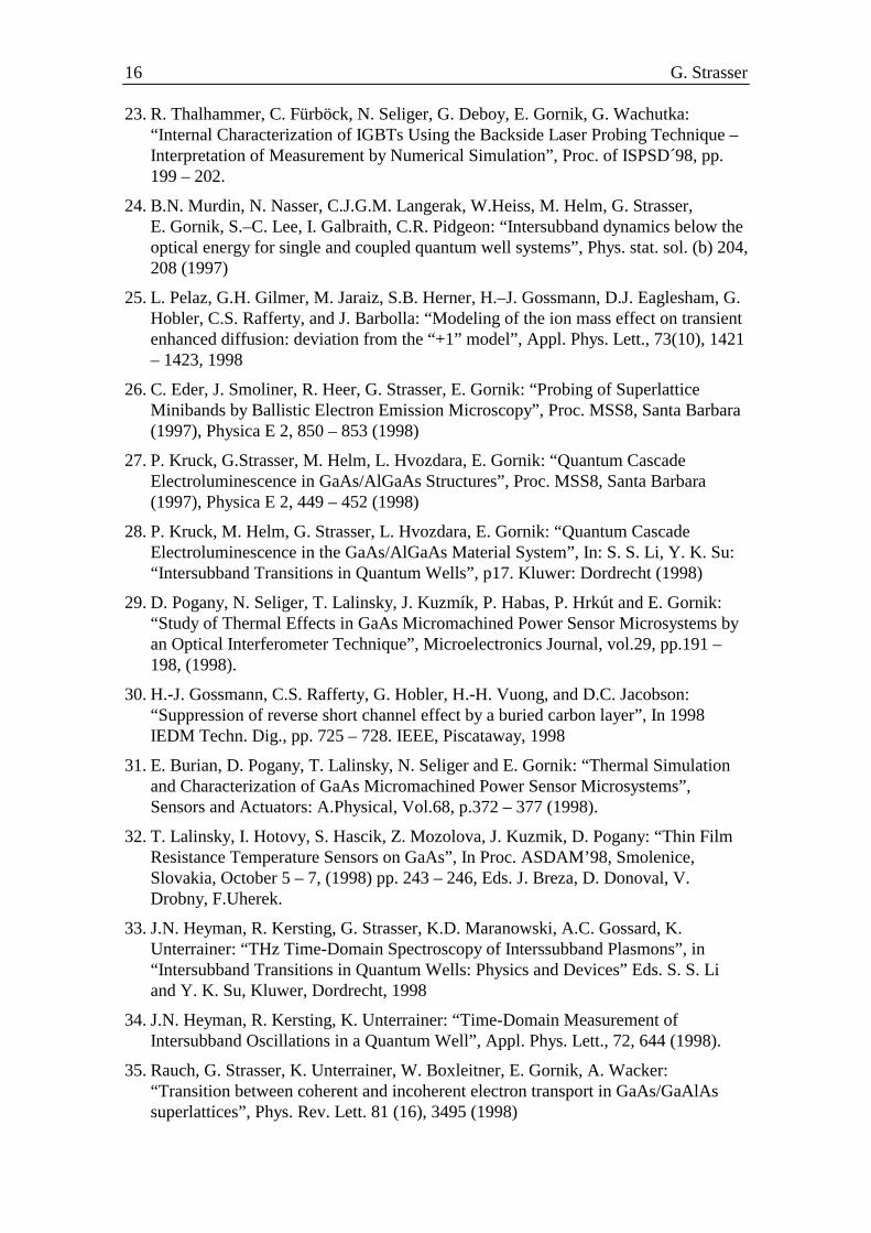
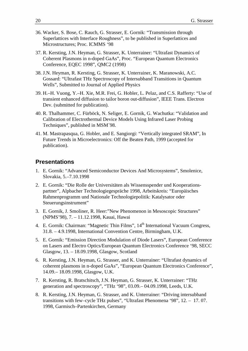
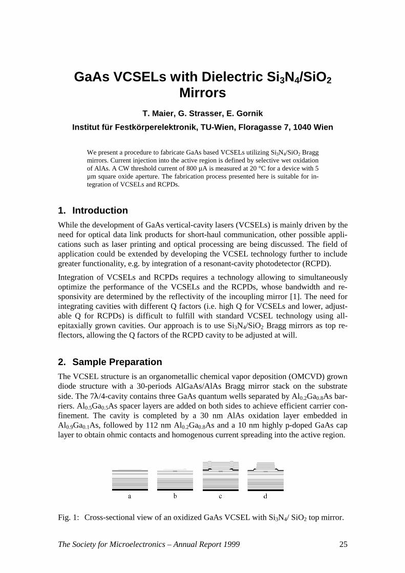
Fig. 1: Cross-sectional view of an oxidized GaAs VCSEL with Si3N4/ SiO2 top mirror.
26 T. Maier et al.
A broad area Sn/Au contact is deposited at the backside of the substrate and annealed at380 °C. The top layers are etched to form shallow square mesas exposing the AlAs oxi-dation layer (Fig. 1a) which is subsequently oxidized in a furnace set at 520 °C (Fig.1b). In situ optical monitoring is used to stop the oxidation process. Electrical contact ismade to the p-type GaAs surface using Cr/Au metallization (Fig. 1c). The top Braggmirror is deposited by plasma enhanced chemical vapor deposition (PECVD) and con-sists of 16 pairs Si3N4/ SiO2 (Fig. 1c). It has already been shown that these mirrors meetthe demands on reflectivity for use in VCSELs [2]. A two-step etching process is usedto pattern the top mirror (Fig. 1d): the first step, Ar-ion etching, is stopped approxi-mately 50 nm above the metallization, the remaining dielectric is then removed in a re-active ion etch process which exposes the extended contacts of the devices.
RCPDs with an area of 50 µm square were integrated beside the VCSELs, but have notbeen investigated so far. Tuning the RCPDs to the desired bandwidth and responsivitycan be accomplished by removing excessive mirror pairs in a further etch step.
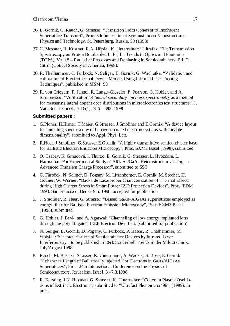
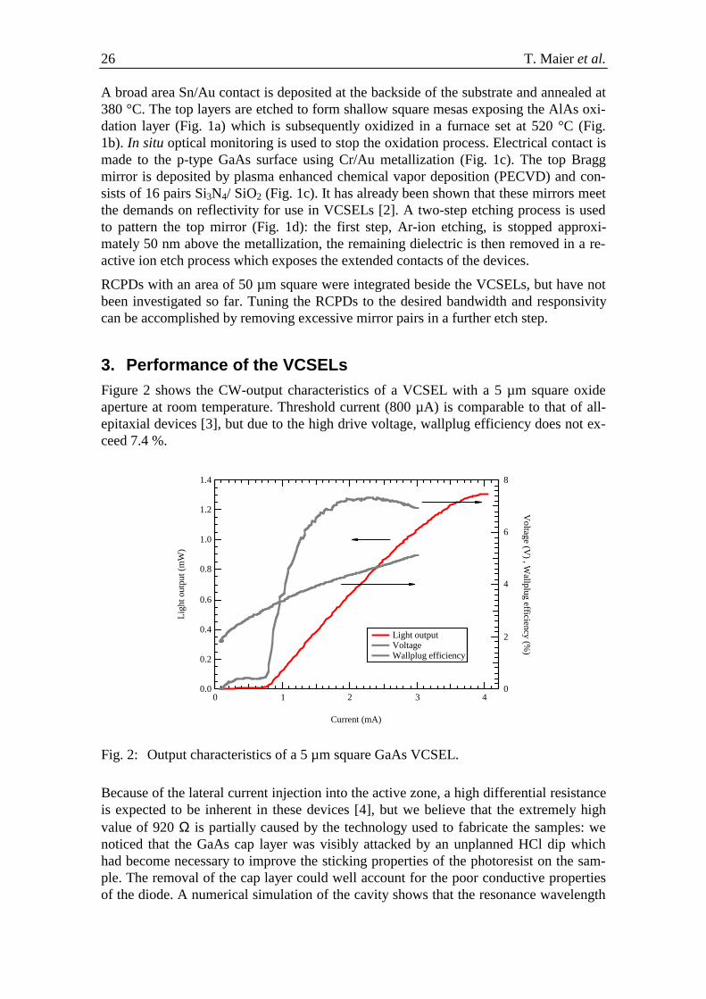
3. Performance of the VCSELsFigure 2 shows the CW-output characteristics of a VCSEL with a 5 µm square oxideaperture at room temperature. Threshold current (800 µA) is comparable to that of all-epitaxial devices [3], but due to the high drive voltage, wallplug efficiency does not ex-ceed 7.4 %.
1.4
1.2
1.0
0.8
0.6
0.4
0.2
0.0
Ligh
t out
put (
mW
)
43210
Current (mA)
8
6
4
2
0
Voltage (V
) , Wallplug efficiency (%
)
Light output Voltage Wallplug efficiency
Fig. 2: Output characteristics of a 5 µm square GaAs VCSEL.
Because of the lateral current injection into the active zone, a high differential resistanceis expected to be inherent in these devices [4], but we believe that the extremely highvalue of 920 Ω is partially caused by the technology used to fabricate the samples: wenoticed that the GaAs cap layer was visibly attacked by an unplanned HCl dip whichhad become necessary to improve the sticking properties of the photoresist on the sam-ple. The removal of the cap layer could well account for the poor conductive propertiesof the diode. A numerical simulation of the cavity shows that the resonance wavelength
GaAs VCSELs with Dielectric Si3N4/SiO2 Mirrors 27
is blue shifted by approximately 6 nm if the cap layer is missing. This is in good agree-ment with the observed laser wavelength of 843.5 nm as opposed to the design wave-length of 850 nm.
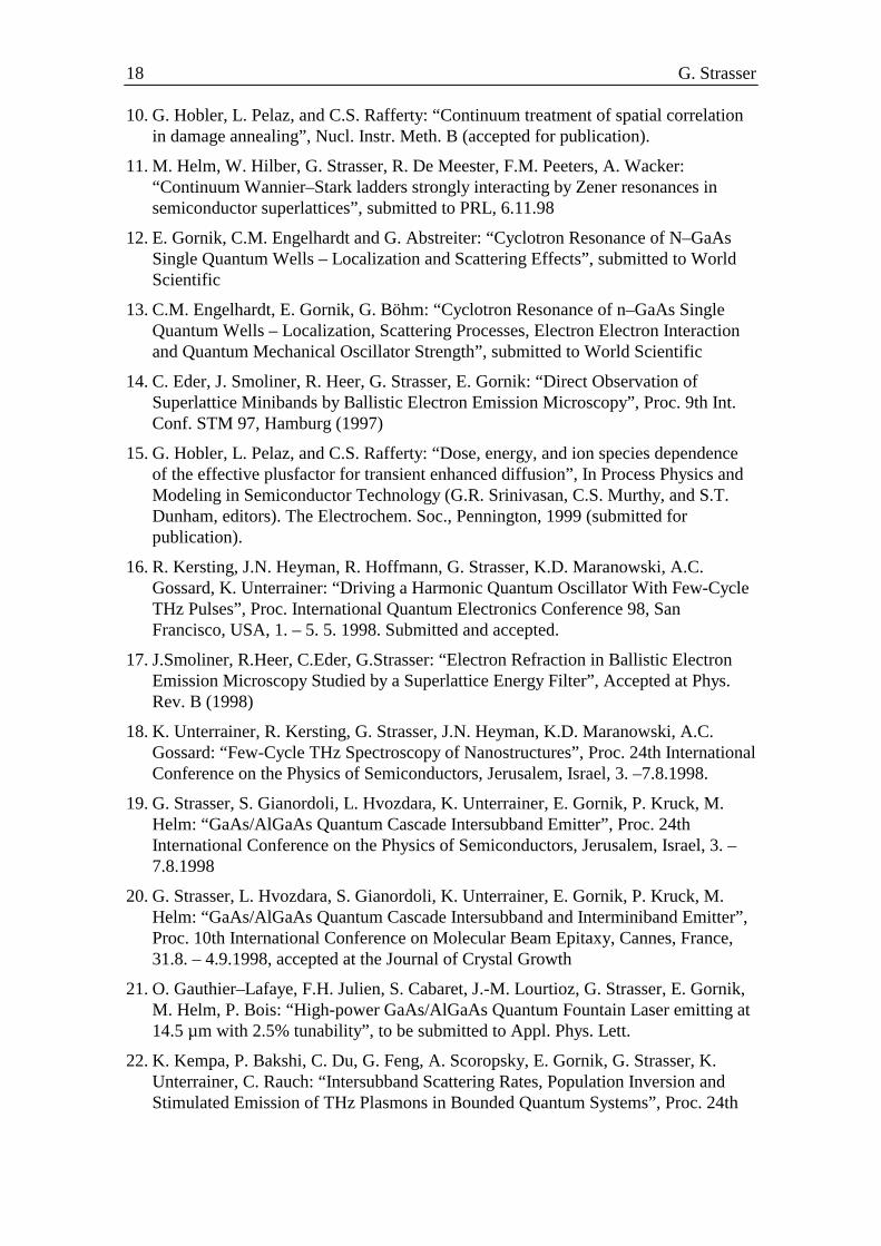
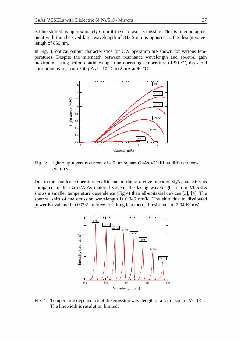
In Fig. 3, optical output characteristics for CW operation are shown for various tem-peratures. Despite the mismatch between resonance wavelength and spectral gainmaximum, lasing action continues up to an operating temperature of 90 °C, thresholdcurrent increases from 750 µA at –10 °C to 2 mA at 90 °C.
1.6
1.4
1.2
1.0
0.8
0.6
0.4
0.2
0.0
Ligh
t out
put (
mW
)
43210
Current (mA)
+90 °C
+70 °C
+50 °C
+30 °C
+10 °C
-10 °C
Fig. 3: Light output versus current of a 5 µm square GaAs VCSEL at different tem-peratures.
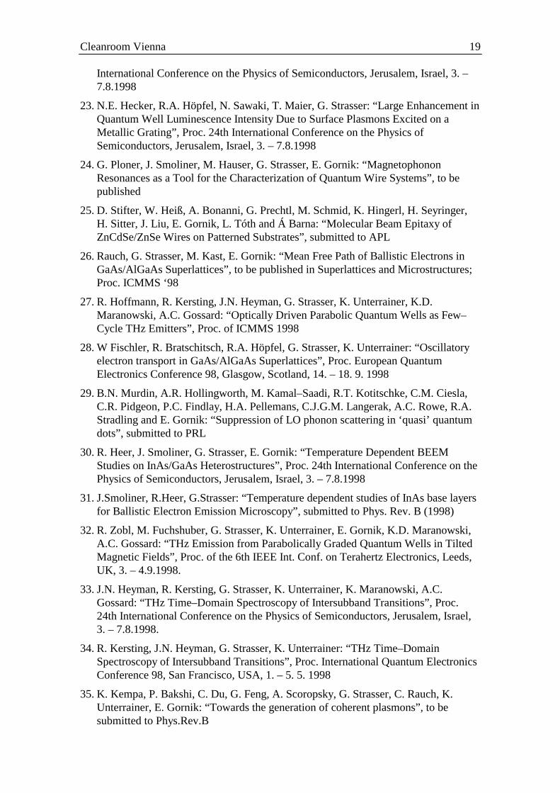
Due to the smaller temperature coefficients of the refractive index of Si3N4 and SiO2 ascompared to the GaAs/AlAs material system, the lasing wavelength of our VCSELsshows a smaller temperature dependence (Fig 4) than all-epitaxial devices [3], [4]. Thespectral shift of the emission wavelength is 0.045 nm/K. The shift due to dissipatedpower is evaluated to 0.092 nm/mW, resulting in a thermal resistance of 2.04 K/mW.
Inte
nsity
(ar
b. u
nits
)
846845844843842
Wavelength (nm)
0 °C
10 °C20 °C
30 °C40 °C
50 °C
60 °C
70 °C
Fig. 4: Temperature dependence of the emission wavelength of a 5 µm square VCSEL.The linewidth is resolution limited.
28 T. Maier et al.
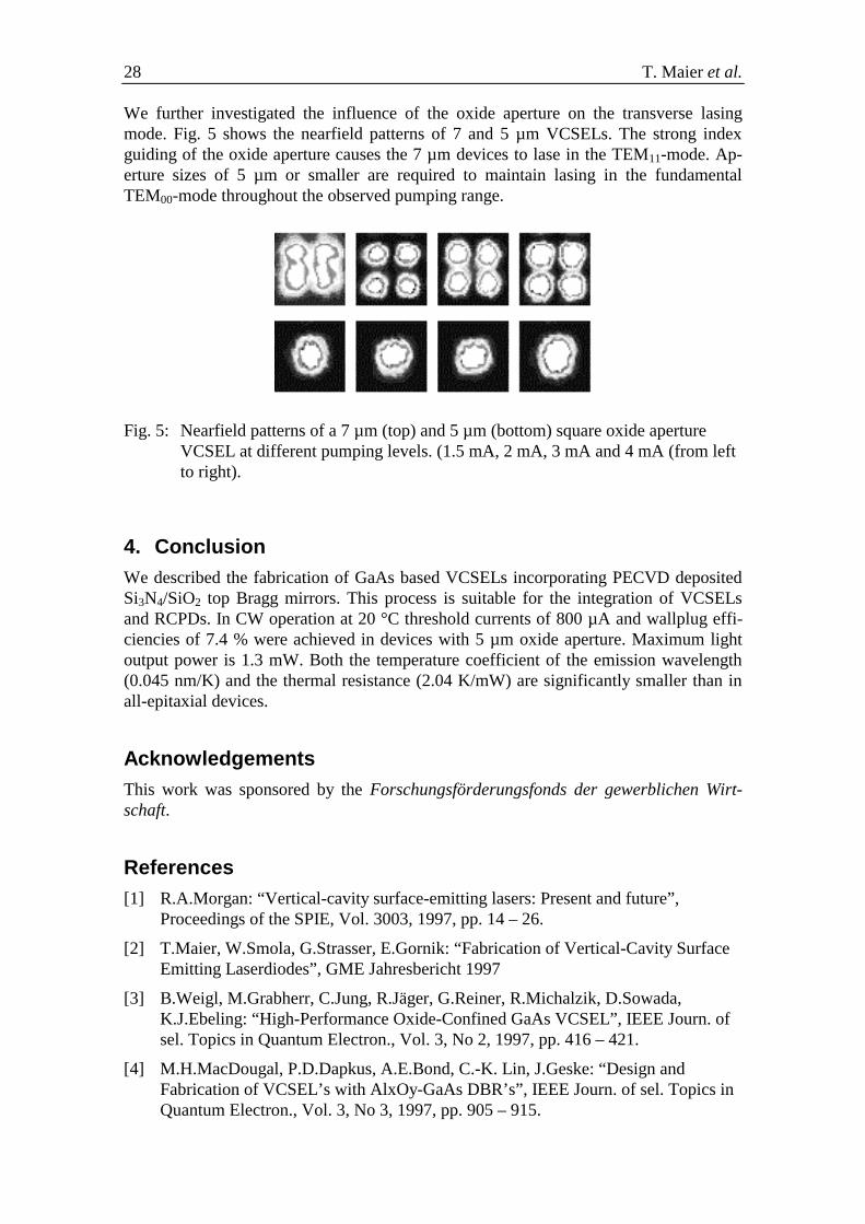
We further investigated the influence of the oxide aperture on the transverse lasingmode. Fig. 5 shows the nearfield patterns of 7 and 5 µm VCSELs. The strong indexguiding of the oxide aperture causes the 7 µm devices to lase in the TEM11-mode. Ap-erture sizes of 5 µm or smaller are required to maintain lasing in the fundamentalTEM00-mode throughout the observed pumping range.
Fig. 5: Nearfield patterns of a 7 µm (top) and 5 µm (bottom) square oxide apertureVCSEL at different pumping levels. (1.5 mA, 2 mA, 3 mA and 4 mA (from leftto right).
4. ConclusionWe described the fabrication of GaAs based VCSELs incorporating PECVD depositedSi3N4/SiO2 top Bragg mirrors. This process is suitable for the integration of VCSELsand RCPDs. In CW operation at 20 °C threshold currents of 800 µA and wallplug effi-ciencies of 7.4 % were achieved in devices with 5 µm oxide aperture. Maximum lightoutput power is 1.3 mW. Both the temperature coefficient of the emission wavelength(0.045 nm/K) and the thermal resistance (2.04 K/mW) are significantly smaller than inall-epitaxial devices.
AcknowledgementsThis work was sponsored by the Forschungsförderungsfonds der gewerblichen Wirt-schaft.
References[1] R.A.Morgan: “Vertical-cavity surface-emitting lasers: Present and future”,
Proceedings of the SPIE, Vol. 3003, 1997, pp. 14 – 26.
[2] T.Maier, W.Smola, G.Strasser, E.Gornik: “Fabrication of Vertical-Cavity SurfaceEmitting Laserdiodes”, GME Jahresbericht 1997
[3] B.Weigl, M.Grabherr, C.Jung, R.Jäger, G.Reiner, R.Michalzik, D.Sowada,K.J.Ebeling: “High-Performance Oxide-Confined GaAs VCSEL”, IEEE Journ. ofsel. Topics in Quantum Electron., Vol. 3, No 2, 1997, pp. 416 – 421.
[4] M.H.MacDougal, P.D.Dapkus, A.E.Bond, C.-K. Lin, J.Geske: “Design andFabrication of VCSEL’s with AlxOy-GaAs DBR’s”, IEEE Journ. of sel. Topics inQuantum Electron., Vol. 3, No 3, 1997, pp. 905 – 915.
The Society for Microelectronics – Annual Report 1999 29
GaAs/AlGaAs/InGaAs Bandgap Lasers —From DH Lasers to VCSELs
W. Schrenk, N. Finger, T. Maier, P. O. Kellermann, G. Strasser, E. Gornik
Institut für Festkörperelektronik, TU-WienMikrostrukturzentrum der TU-WienFloragasse7, A-1040 Wien, Austria
Starting from the growth of double hetero (DH) semiconductor bandgap lasers, in thematerial system AlGaAs/GaAs we are now optimizing laser devices such as a twinwaveguide laser and a laser interferometer based on vertical cavity surface emittinglasers (VCSEL).
1. MBEMBE (molecular beam epitaxy) technique allows the epitaxial growth of different com-pounds. One of the model materials for optoelectronics are epitaxial layers of III-Vsemiconductors, mainly GaAs and related compounds. The controlled growth of singlecrystalline layers on an atomic scale makes it possible to design new materials with op-timized electrical and optical characteristics. A solid source MBE system (MOD GENII) is used for the growth of AlGaAs/GaAs semiconductor lasers and InGaAs quantumwell lasers; thus, this machine is further equipped with an indium cell. As doping mate-rials we use silicon for n-doping and carbon for p-doping.
2. LasersWe started laser growth with double hetero (DH) GaAs/AlGaAs laser structures. Thismaterial was characterized by processing broad area lasers and measuring their electricaland optical properties. The threshold current density and differential efficiency are com-parable to lasers processed from industrial grown materials [1].
870 871 872 873
0,0
0,2
0,4
0,6
0,8
1,0
dλ/dT = 0.05 nm/K
T heat sink: 5, 10, 15, 20, 25° C
Inte
nsi
ty (
arb
. un
its)
λ (nm)
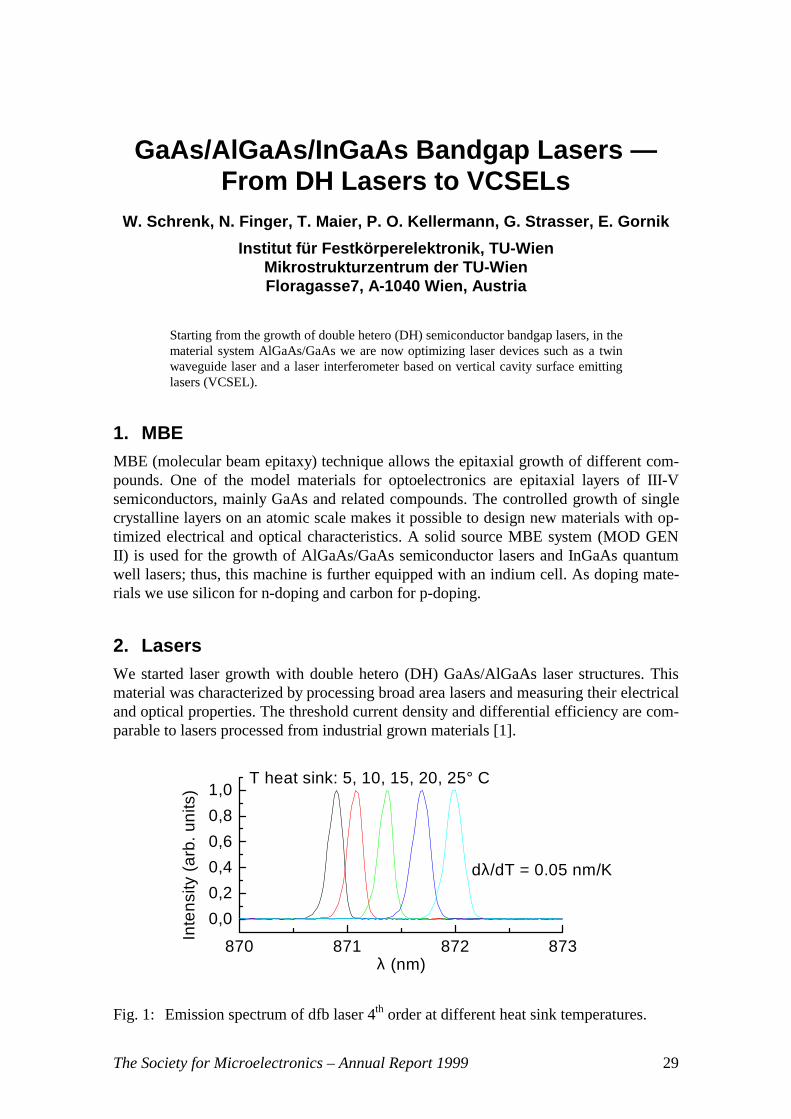
Fig. 1: Emission spectrum of dfb laser 4th order at different heat sink temperatures.
30 W. Schrenk et al
As a next step, ridge lasers were processed out of DH material. The ridge forms a lateraloptical waveguide, which allows the realization of single mode lasers, where in additiona longitudinal mode control is needed. A simple model for calculating the lateral opticalwaveguide is the effective index model. The difference of the effective transverse re-fractive index and the width of the ridge determines how many lateral waveguide modesare possible and the divergence of the facet emission in lateral direction. Based on theridge laser design we started to manufacture “single mode lasers” by incorporating alongitudinal mode control via a 4th order dfb (distributed feed back) grating. The reasonfor choosing a 4th order grating (period 515 nm) at this time was the established holo-graphic grating definition with our HeCd laser setup for this grating period. The meas-ured lasers showed a drift in the emission wavelength of about 0.05 nm/K, as can beseen in Fig. 1 (linewidth limited by the used spectrometer) due to change of the refrac-tive index with temperature, which is in good agreement with literature [2].
As a next step, InGaAs SQW (single quantum well) lasers with separate confinementlayers were grown. Strained InGaAs QWs show higher peak material gain than un-strained QWs or bulk material. The lattice mismatch between GaAs and InGaAs deter-mines the so-called critical thickness for InGaAs layers on GaAs. Layers thinner thanthe critical thickness can be grown without relaxation effects. There are different modelsfor calculating the critical thickness, e.g. by Matthews and Blakeslee or People and Bean[3]. One difficulty in the growth of strained InGaAs layers on GaAs is the calibration ofIn content and growth rate with RHEED (reflected high energy electron diffraction)measurements, originating from the lattice mismatch of the two materials. Additionally,optical problems remain in InGaAs QW lasers due to the large antiguiding effect and thenonlinear gain behavior at high current densities. E.g. the current density for narrowgain guided lasers increases dramatically for widths below 20 µm [3]. Therefore, a rela-tively strong index guiding is needed for narrow lasers. The grown SQW material wascharacterized with broad area lasers and showed threshold densities comparable to stateof the art lasers [4], [5]. Ridge lasers with widths from 2 µm to 6 µm show kink-freelight output (fig. 2) up to current densities of 5 times threshold density (limited by thesetup) and the measured far field pattern indicates that only one lateral mode exists.
0 20 40 60 80 100
0
5
10
15
20
25
30laser InGaAs SQWw = 4 µml = 920 µm
P (
mW
) pe
r fa
cet
I (mA)
Fig. 2: Emitted power versus injected current of an InGaAs SQW laser (ridge width4 µm).
GaAs/AlGaAs/InGaAs Bandgap Lasers 31
Currently we are working on two laser projects, a twin waveguide laser and a laser inter-ferometer.
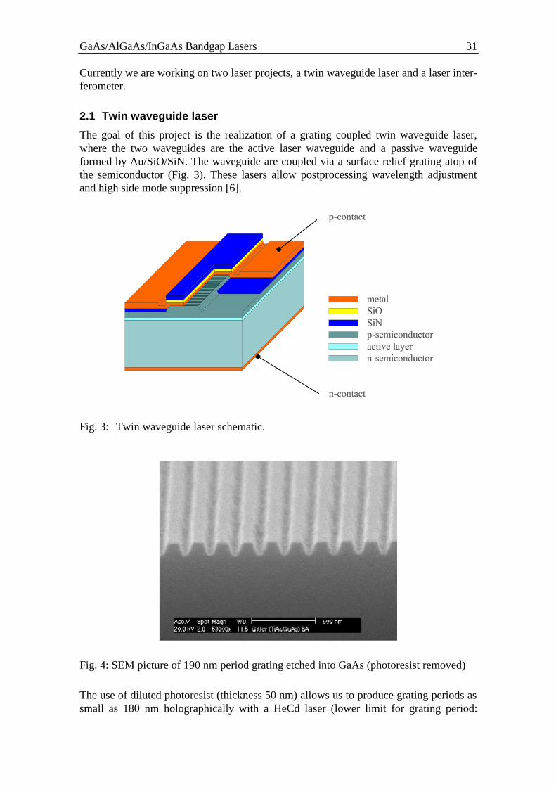
2.1 Twin waveguide laser
The goal of this project is the realization of a grating coupled twin waveguide laser,where the two waveguides are the active laser waveguide and a passive waveguideformed by Au/SiO/SiN. The waveguide are coupled via a surface relief grating atop ofthe semiconductor (Fig. 3). These lasers allow postprocessing wavelength adjustmentand high side mode suppression [6].
Fig. 3: Twin waveguide laser schematic.
Fig. 4: SEM picture of 190 nm period grating etched into GaAs (photoresist removed)
The use of diluted photoresist (thickness 50 nm) allows us to produce grating periods assmall as 180 nm holographically with a HeCd laser (lower limit for grating period:
32 W. Schrenk et al
325 nm/2 = 162.5 nm) in standard resist material. The used InGaAs QW laser materialfor the twin waveguide laser is designed for emission at about 980 nm, thus needing agrating period of about 190 nm, which is accessible with our setup as shown in Fig. 4.
2.2 Laser interferometer
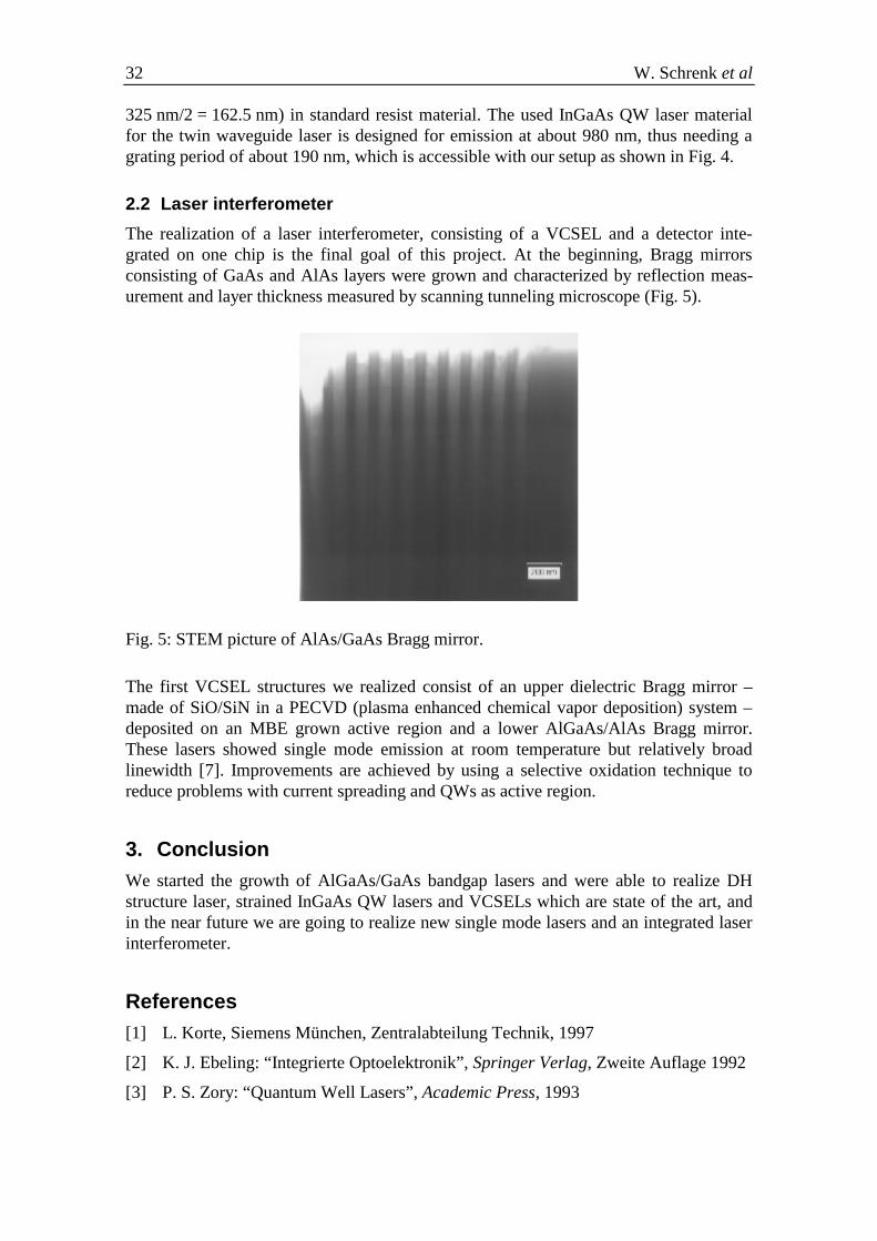
The realization of a laser interferometer, consisting of a VCSEL and a detector inte-grated on one chip is the final goal of this project. At the beginning, Bragg mirrorsconsisting of GaAs and AlAs layers were grown and characterized by reflection meas-urement and layer thickness measured by scanning tunneling microscope (Fig. 5).
Fig. 5: STEM picture of AlAs/GaAs Bragg mirror.
The first VCSEL structures we realized consist of an upper dielectric Bragg mirror –made of SiO/SiN in a PECVD (plasma enhanced chemical vapor deposition) system –deposited on an MBE grown active region and a lower AlGaAs/AlAs Bragg mirror.These lasers showed single mode emission at room temperature but relatively broadlinewidth [7]. Improvements are achieved by using a selective oxidation technique toreduce problems with current spreading and QWs as active region.
3. ConclusionWe started the growth of AlGaAs/GaAs bandgap lasers and were able to realize DHstructure laser, strained InGaAs QW lasers and VCSELs which are state of the art, andin the near future we are going to realize new single mode lasers and an integrated laserinterferometer.
References[1] L. Korte, Siemens München, Zentralabteilung Technik, 1997
[2] K. J. Ebeling: “Integrierte Optoelektronik”, Springer Verlag, Zweite Auflage 1992
[3] P. S. Zory: “Quantum Well Lasers”, Academic Press, 1993

GaAs/AlGaAs/InGaAs Bandgap Lasers 33
[4] S. Y. Hu, D. B. Young, A. C. Gossard, L. A. Coldren: “The Effect of LateralLeakage Current on the Experimental Gain/Current-Density Curve in Quantum-Well Ridge-Waveguide Lasers”, IEEE Journal of Quant. Elect., Vol. 30 (10),1994, pp. 2245 – 2250
[5] M. Micovic, P. Evaldsson, M. Geva, G. W. Taylor, T. Vang, R. J. Malik:“Quantum well lasers with carbon doped cladding layers grown by solid sourcemolecular beam epitaxy”, Appl. Phys. Lett., Vol. 64 (4), 1994, pp. 411 - 413
[6] N. Finger, E. Gornik: “Analysis of metallized -grating twin-waveguide structures”,IEEE J. Quantum Electron., submitted for publication, 1998
[7] T. Maier, W. Smola, G. Strasser, E. Gornik: “ Fabrication of Vertical-CavitySurface Emitting Laserdiodes”, GMe Jahresbericht 1997

The Society for Microelectronics – Annual Report 1999 35
Wavelength Adjustable Surface EmittingSingle Mode Laser Diodes with
Contradirectional Surface Mode CouplingP. O. Kellermann, N. Finger, W. Schrenk, and E. Gornik
Institut für Festkörperelektronik, TU-Wien, Floragasse 7, A-1040 Wien
H.-P. Gauggel, R. Winterhoff, and M.H. Pilkuhn
4. Physik. Institut, Univ. Stuttgart, Pfaffenwaldring 57, D-70550 Stuttgart
Single-mode surface emission has been achieved from visible red GaInP/AlGaInPlaser diodes by applying the contradirectional surface mode coupling technique. Theemission wavelength (≈ 679.5 nm) of the laser structures was adjusted (decreased) insteps of 0.2 nm in an interval of 1.5 nm by reducing the thickness of the waveguideon top of the laser diode. The laser diodes emitted via the surface with a beam diver-gence of 0.10° and showed single-mode emission both in AC as well as in DC op-eration with a minimum spectral linewidth of 0.09 nm. The highest sidemode sup-pression achieved in DC operation was 26 dB.
1. IntroductionSemiconductor laser diodes in the visible regime are very suitable to be employed aspowerful emitters in optical short-range data transmission (the attenuation minimum ofpolymethylmethacrylate (PMMA) fibers lies near 650 nm) and as light sources in thenext generation of optical disk drives with their ability to read and write highly con-densed optical information. The field of applications is widely spread, including spec-troscopy, displays and optical sensing. Several red laser-diode-configurations have beensuccessfully realized so far by using GaxIn1-xP/(AlyGa1-y)0.5In0.5P sample structures. Ex-cellent laser emission with low threshold current and high output power in the wave-length range between 620 and 690 nm has been reported.
Improvement of the emission characteristics and flexibility of the emission wavelengthis desirable for advanced technical usage. If one achieves laser diodes with several sin-gle-mode emission spectra near the attenuation minimum of the optical fiber, the trans-mission bit rate of communication systems can be increased significantly by densewavelength division multiplexing (DWDM) as the heart of multiwavelength optical net-working (MONET). If surface emission (emission vertically to the epitaxially grownlayers) is accomplished, the beam divergence is decreased essentially due to the ex-panded outcoupling window. Surface emission also eases the fabrication of two-dimensional arrays and the integration with the driving circuit on the same wafer.
Several concepts for obtaining single-mode surface emission have been presented byusing second-order grating distributed feedback DFB lasers. They use the incorporationof a phase-shifting film [1], preferential current pumping [2], the effect of chirping thegrating structure [3] or a complex-coupled grating [4]. There is no beam steering effectdue to wavelength and temperature variations, since the beam direction is fixed by the
36 P. O. Kellermann et al.
DFB grating structure. Wavelength shift in DFB laser arrays is achieved by changing thegrating period of the individual elements requiring a very precise definition of the grat-ing period to achieve a well defined emission wavelength. But there have been no pa-pers reporting about the realization of these concepts in the red wavelength regime. Incontrast the red vertical cavity surface emitting laser (VCSEL) diodes [5], [6], withwhich large-signal modulation of 1.5 Gb/s has been demonstrated. A wavelength shiftcan be achieved by generating a thickness gradient across the wafer during epitaxialgrowth [7].
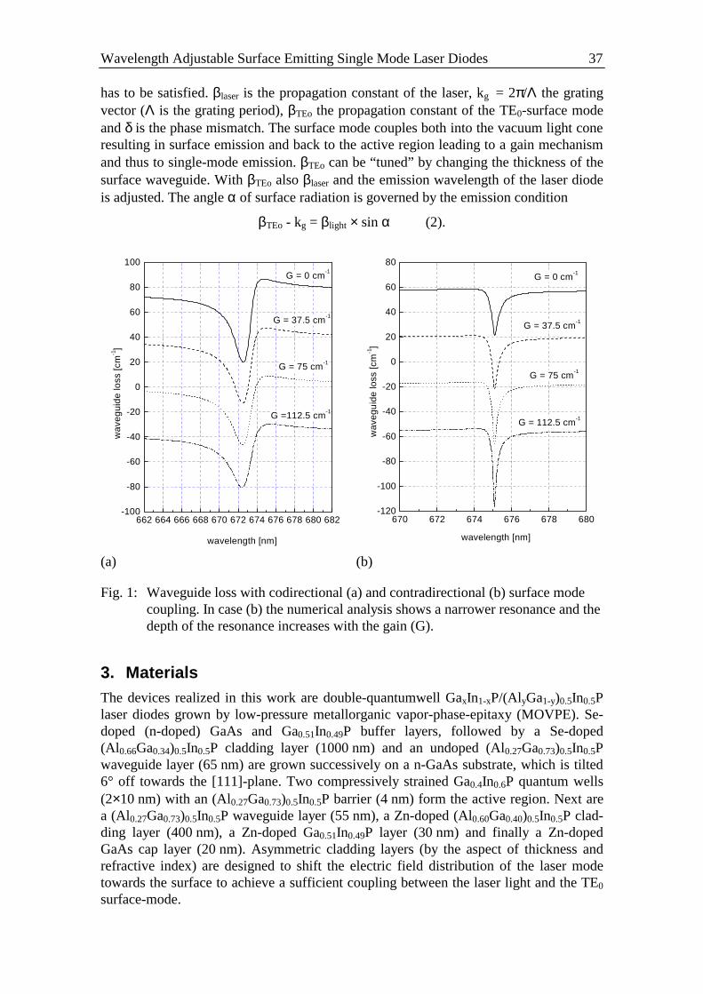
2. MethodsWe have developed a method to achieve single-mode surface emission from horizontalcavity laser diodes, which is based on surface mode coupling (SMC). The laser diodecharacteristics (wavelength, emission-angle) can be adjusted after the processing as alaser diode by changing only the surface parameters (waveguide’s optical thickness).This leads to a straight way of creating multi wavelength laser diode arrays [8]. As SMClaser diodes can be fabricated by using the established technique of the conventionalstripe-contact laser the complex fabrication process of VCSEL structures and of DFBlasers is avoided. The principle of these laser diodes is based on a coupling mechanismbetween the laser mode and the surface mode which exists in a semitransparentmetal/dielectricum waveguide structure on top of the laser diode. Phase matching of thelaser mode and the surface mode is achieved by a surface relief grating in the laser di-ode. The grating causes radiation losses of the laser mode, which are reduced signifi-cantly only in a narrow spectral range by the excitation and feed back process of thesurface mode. The effective gain mechanism of this resonance leads to single modeemission. Recently we have shown that the SMC technique with codirectional (the lasermode and the surface mode are propagating in the same direction) coupling can be ap-plied to GaAs/AlGaAs and to GaInP/AlGaInP laser diodes to achieve both a single-mode emission as well as a surface emission with very narrow beam divergence [9],[10]. The radiation and the longitudinal mode characteristics of the waveguide gratingstructures have been investigated numerically with an in-depth analysis based on theFloquet-Bloch theory. The numerical analysis shows that in case of contradirectional(the laser mode and the surface mode are counterpropagating) coupling between thelaser mode and the surface mode the sidemode suppression of the emission wavelengthis increased compared to the codirectional coupling mechanism due to a narrower reso-nance. In Fig. 1 the waveguide loss with co- and contradirectional surface mode cou-pling is shown. In case of contradirectional coupling the depth of the resonance in-creases with the gain. The contradirectional surface mode coupling concept has nowbeen realized for the first time.
The physical background of the SMC-concept with surface emission and with contradi-rectional coupling is the following: the laser light propagating in the active region isexciting a transverse electrically polarized (TE0) surface mode in a waveguide structureon the top of the laser diode through a 2nd order grating coupling. Therefore the phasematching condition
βlaser – 2 × kg = βTEo + δ (1)
Wavelength Adjustable Surface Emitting Single Mode Laser Diodes 37
has to be satisfied. βlaser is the propagation constant of the laser, kg = 2π/Λ the gratingvector (Λ is the grating period), βTEo the propagation constant of the TE0-surface modeand δ is the phase mismatch. The surface mode couples both into the vacuum light coneresulting in surface emission and back to the active region leading to a gain mechanismand thus to single-mode emission. βTEo can be “tuned” by changing the thickness of thesurface waveguide. With βTEo also βlaser and the emission wavelength of the laser diodeis adjusted. The angle α of surface radiation is governed by the emission condition
βTEo - kg = βlight × sin α (2).
662 664 666 668 670 672 674 676 678 680 682-100
-80
-60
-40
-20
0
20
40
60
80
100
G =112.5 cm-1
G = 75 cm-1
G = 37.5 cm-1
G = 0 cm-1
wa
veg
uid
e lo
ss [c
m-1]
wavelength [nm]
670 672 674 676 678 680-120
-100
-80
-60
-40
-20
0
20
40
60
80
G = 0 cm-1
G = 112.5 cm-1
G = 37.5 cm-1
G = 75 cm-1
wavelength [nm]
wav
egu
ide
loss
[cm
-1]
(a) (b)
Fig. 1: Waveguide loss with codirectional (a) and contradirectional (b) surface modecoupling. In case (b) the numerical analysis shows a narrower resonance and thedepth of the resonance increases with the gain (G).
3. MaterialsThe devices realized in this work are double-quantumwell GaxIn1-xP/(AlyGa1-y)0.5In0.5Plaser diodes grown by low-pressure metallorganic vapor-phase-epitaxy (MOVPE). Se-doped (n-doped) GaAs and Ga0.51In0.49P buffer layers, followed by a Se-doped(Al0.66Ga0.34)0.5In0.5P cladding layer (1000 nm) and an undoped (Al0.27Ga0.73)0.5In0.5Pwaveguide layer (65 nm) are grown successively on a n-GaAs substrate, which is tilted6° off towards the [111]-plane. Two compressively strained Ga0.4In0.6P quantum wells(2×10 nm) with an (Al0.27Ga0.73)0.5In0.5P barrier (4 nm) form the active region. Next area (Al0.27Ga0.73)0.5In0.5P waveguide layer (55 nm), a Zn-doped (Al0.60Ga0.40)0.5In0.5P clad-ding layer (400 nm), a Zn-doped Ga0.51In0.49P layer (30 nm) and finally a Zn-dopedGaAs cap layer (20 nm). Asymmetric cladding layers (by the aspect of thickness andrefractive index) are designed to shift the electric field distribution of the laser modetowards the surface to achieve a sufficient coupling between the laser light and the TE0
surface-mode.
38 P. O. Kellermann et al.
The second-order grating (duty cycle 0.67) for surface mode coupling is defined byholographic exposure of a spin-coated photoresist (Hoechst AZ 5214) on the p-side ofthe laser structure. The pattern is etched into the top layers by ion milling (period Λ =270 nm, height H = 100 nm). The evaporation of semitransparent Au/Zn/Au metalstripes (thickness 5 nm/5 nm/20 nm) with a width of 12.4 µm defines the stripe contactsof the lasers. Ti/Au contact pads (50 nm/250 nm), which overlap the laser stripe contactby 3.7 µm from both sides leaving a 5 µm wide window in the center of the laser stripecontact, are evaporated on a polymid isolation in between the single stripe contacts.Next the laser stripe is coated with two dielectric layers (~150 nm SiOx ( 5.1=n ) below~250 nm SiNx ( 9.1=n )) forming a slab waveguide on the top of the laser diode, whichsupports the TE0-surface-mode. The combination of low-index and high-index dielectricis utilized in order to avoid excessive leakage losses into the high-index substrate. Fi-nally, the laser bars are cleaved to a length between 350 µm and 500 µm and mountedon a Peltier element.
4. ResultsThe SMC laser diodes showed a threshold current density (jth) of 1 kA/cm2 at a tem-perature of 10°C in pulsed driven (AC) and at –5°C in continuos wave (DC) operation.The series resistance of the laser diodes was near 9 Ω.
The farfield pattern of the laser diodes was measured by scanning from one cleavedfacet along the laser stripe-contact to the other facet. The surface emission was observedat ±50° with a beam divergence of 0.10°. The divergence in the perpendicular directionwas 10°. The intensity emitted per solid angle into the single surface beam was threetimes larger than the emitted intensity per solid angle at the edges.
673 674 675 676 677 678 679 680 681 682 683
1E-3
0.01
0.1
1
inte
nsi
ty [
arb
. u
nits
]
wavelength [nm]
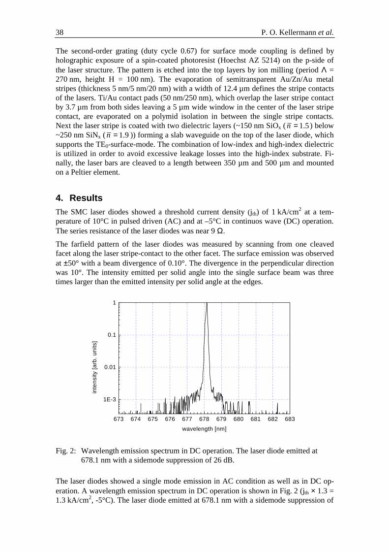
Fig. 2: Wavelength emission spectrum in DC operation. The laser diode emitted at678.1 nm with a sidemode suppression of 26 dB.
The laser diodes showed a single mode emission in AC condition as well as in DC op-eration. A wavelength emission spectrum in DC operation is shown in Fig. 2 (jth × 1.3 =1.3 kA/cm2, -5°C). The laser diode emitted at 678.1 nm with a sidemode suppression of
Wavelength Adjustable Surface Emitting Single Mode Laser Diodes 39
26 dB. The minimum spectral linewidth achieved was 0.09 nm (spectrometer resolution0.07 nm). The longitudinal mode separation of the Fabry-Perot cavity was measured tobe 0.11 nm.
676 677 678 679 680 6810
500
1000
1500
2000in
ten
sity
[arb
. uni
ts]
wavelength [nm]
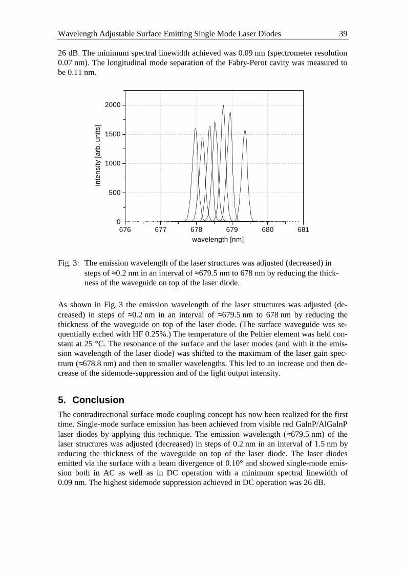
Fig. 3: The emission wavelength of the laser structures was adjusted (decreased) insteps of ≈0.2 nm in an interval of ≈679.5 nm to 678 nm by reducing the thick-ness of the waveguide on top of the laser diode.
As shown in Fig. 3 the emission wavelength of the laser structures was adjusted (de-creased) in steps of ≈0.2 nm in an interval of ≈679.5 nm to 678 nm by reducing thethickness of the waveguide on top of the laser diode. (The surface waveguide was se-quentially etched with HF 0.25%.) The temperature of the Peltier element was held con-stant at 25 °C. The resonance of the surface and the laser modes (and with it the emis-sion wavelength of the laser diode) was shifted to the maximum of the laser gain spec-trum (≈678.8 nm) and then to smaller wavelengths. This led to an increase and then de-crease of the sidemode-suppression and of the light output intensity.
5. ConclusionThe contradirectional surface mode coupling concept has now been realized for the firsttime. Single-mode surface emission has been achieved from visible red GaInP/AlGaInPlaser diodes by applying this technique. The emission wavelength (≈679.5 nm) of thelaser structures was adjusted (decreased) in steps of 0.2 nm in an interval of 1.5 nm byreducing the thickness of the waveguide on top of the laser diode. The laser diodesemitted via the surface with a beam divergence of 0.10° and showed single-mode emis-sion both in AC as well as in DC operation with a minimum spectral linewidth of0.09 nm. The highest sidemode suppression achieved in DC operation was 26 dB.
40 P. O. Kellermann et al.
AcknowledgementsThis work is partly supported by the Volkswagen-Stiftung (Germany).
References[1] S. H. Macomber, J. S. Mott, H. F. Chung, and T. L. Paoli, Proc. SPIE 1219, 228
(1990)
[2] N. W. Carlson, S. K. Liew, R. Amantea, D. P. Bour, G. A. Evans, and E. A.Vangieson, IEEE J. Quantum Electron. QE-27, 1746 (1991)
[3] S. H. Macomber, IEEE J. Quantum Electron. QE-26, 2065 (1990)
[4] M. Kasraian and D. Botez, Appl. Phys. Lett. 69, 2795 (1996)
[5] R. P. Schneider, Jr. , and J. A. Lott, Appl. Phys. Lett. 63, 917 (1993)
[6] R. P. Schneider, Jr. , M. Hagerott Crawford, K. D. Choquette, K. L. Lear, S. P.Kilcoyne, and J. J. Figiel, Appl. Phys. Lett. 67, 329 (1995)
[7] C.J. Chang-Hasnain, J.P. Harbinson, C.E. Zah, M.W. Maeda, L.T. Florez, N.G.Stoffel, T.P. Lee: IEEE J. Quantum Electron., vol. QE-27, 1368, (1991)
[8] A. Golshani, P.O. Kellermann, A. Köck, E. Gornik, and L. Korte, Appl. Phys. Lett.70 (6), 762-764, (1997)
[9] A. Köck, A. Golshani, R. Hainberger, E. Gornik, and L. Korte, Appl. Phys. Lett.69, 3638-3640, (1996)
[10] P.O. Kellermann, A. Golshani, A. Köck, E. Gornik; H.-P. Gauggel, R. Winterhoff,and M.H. Pilkuhn, Appl. Phys. Lett. 70 (18), 2374-2376, (1997)
The Society for Microelectronics – Annual Report 1999 41
GaAs/AlGaAs Based Intersubband andInterminiband Mid-Infrared Emitters
L. Hvozdara, S. Gianordoli, G. Strasser, K. Unterrainer, and E. Gornik
Institut für Festkörperelektronik, TU Wien, Floragasse 7,A-1040 Vienna Austria
Intraband optical transitions in the conduction band of GaAs/AlGaAs heterostruc-tures are used to generate mid-infrared radiation. Bandstructure engineering andepitaxial growth techniques make it possible to tailor the emission wavelength ofmid-IR light emitting diodes over a broad range (6 – 12 micrometer ). We report onthe realization of these emitters, showing two different concepts. The first, intermini-band emitter is based on optical transitions across the minigap of a strong coupledsuperlattice. The second concept is using optical transitions between discrete statesin a system of coupled quantum wells. Emission, photovoltage and transmissionspectra are presented. Self consistent calculations of these structures are performedand compared to the experimental data. The structures are designed to achievepopulation inversion in different subbands of the conduction band.
1. IntroductionEnvironmental monitoring, medicine, and many other technological branches areyearning for compact light sources in Mid-Infrared (MIR) part of the spectrum. The onlycommercially available solid state lasers working in MIR are based on lead-salt semi-conductors. Since the demonstration of the first Quantum Cascade Laser (QCL) by Faistet al (1994) [1] it became a viable source of coherent (MIR) radiation. A significantprogress in the performance and operating characteristics of the QCLs has beenachieved during the last five years. In 1996 operation above room temperature and peakpowers of 100 mW [2], as well as CW operation at 110 K [3] was reported. A distrib-uted feedback (single mode) QCL [4] and tunable QCL [5] were introduced in 1997.Microcylinder QCL with a bow-tie mode is reported in 1998 [6].
All these results have only been reported using a single material system, InGaAs/InAlAslattice matched to InP. The strain requirements limit the composition of the InGaAs andthe InAlAs ternaries. The GaAs/AlGaAs [7] system offers very good lattice match overthe whole range of aluminum content in AlGaAs. Emitters based on this material aredemonstrated [8] and lasing action at cryogenic conditions is achieved [9]. GaAs/AlGaAs is the most common III-V semiconductor material system used in the technol-ogy. Economical aspects of its using are also not negligible, since many possible appli-cations are cost limited which is the only obstacle in their introduction to praxis.
2. Unipolar Quantum Cascade EmittersRadiation in common laser diodes is achieved via radiative recombination of electron-hole pairs across the bandgap. Quantum cascade emitters are using optical transitions ofelectrons between the discrete states within the conduction band of a semiconductorheterostructure. Thus the emitted wavelength is significantly less temperature dependent
L. Hvozdara et al.42
compared to the bandgap emitter. Bandstructure engineering allows tailoring of theemission wavelength to the application requirements over a broad range.
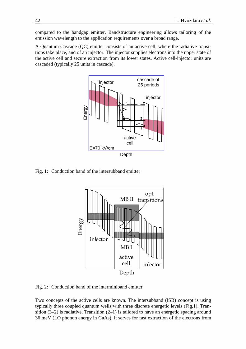
A Quantum Cascade (QC) emitter consists of an active cell, where the radiative transi-tions take place, and of an injector. The injector supplies electrons into the upper state ofthe active cell and secure extraction from its lower states. Active cell-injector units arecascaded (typically 25 units in cascade).
injector
injector
activecell
cascade of 25 periods
Depth
Ene
rgy
E=70 kV/cm
Fig. 1: Conduction band of the intersubband emitter
Fig. 2: Conduction band of the interminiband emitter
Two concepts of the active cells are known. The intersubband (ISB) concept is usingtypically three coupled quantum wells with three discrete energetic levels (Fig.1). Tran-sition (3–2) is radiative. Transition (2–1) is tailored to have an energetic spacing around36 meV (LO phonon energy in GaAs). It serves for fast extraction of the electrons from
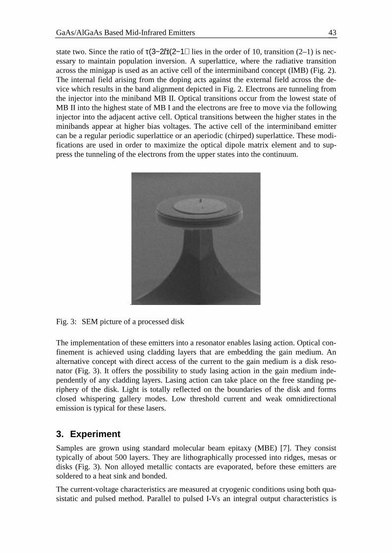
GaAs/AlGaAs Based Mid-Infrared Emitters 43
state two. Since the ratio of τ(3−2)/τ(2−1) lies in the order of 10, transition (2–1) is nec-essary to maintain population inversion. A superlattice, where the radiative transitionacross the minigap is used as an active cell of the interminiband concept (IMB) (Fig. 2).The internal field arising from the doping acts against the external field across the de-vice which results in the band alignment depicted in Fig. 2. Electrons are tunneling fromthe injector into the miniband MB II. Optical transitions occur from the lowest state ofMB II into the highest state of MB I and the electrons are free to move via the followinginjector into the adjacent active cell. Optical transitions between the higher states in theminibands appear at higher bias voltages. The active cell of the interminiband emittercan be a regular periodic superlattice or an aperiodic (chirped) superlattice. These modi-fications are used in order to maximize the optical dipole matrix element and to sup-press the tunneling of the electrons from the upper states into the continuum.
Fig. 3: SEM picture of a processed disk
The implementation of these emitters into a resonator enables lasing action. Optical con-finement is achieved using cladding layers that are embedding the gain medium. Analternative concept with direct access of the current to the gain medium is a disk reso-nator (Fig. 3). It offers the possibility to study lasing action in the gain medium inde-pendently of any cladding layers. Lasing action can take place on the free standing pe-riphery of the disk. Light is totally reflected on the boundaries of the disk and formsclosed whispering gallery modes. Low threshold current and weak omnidirectionalemission is typical for these lasers.
3. ExperimentSamples are grown using standard molecular beam epitaxy (MBE) [7]. They consisttypically of about 500 layers. They are lithographically processed into ridges, mesas ordisks (Fig. 3). Non alloyed metallic contacts are evaporated, before these emitters aresoldered to a heat sink and bonded.
The current-voltage characteristics are measured at cryogenic conditions using both qua-sistatic and pulsed method. Parallel to pulsed I-Vs an integral output characteristics is
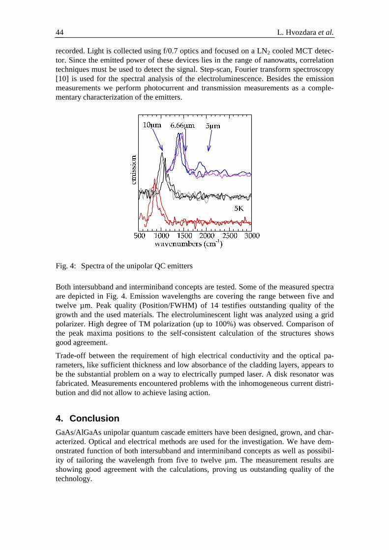
L. Hvozdara et al.44
recorded. Light is collected using f/0.7 optics and focused on a LN2 cooled MCT detec-tor. Since the emitted power of these devices lies in the range of nanowatts, correlationtechniques must be used to detect the signal. Step-scan, Fourier transform spectroscopy[10] is used for the spectral analysis of the electroluminescence. Besides the emissionmeasurements we perform photocurrent and transmission measurements as a comple-mentary characterization of the emitters.
Fig. 4: Spectra of the unipolar QC emitters
Both intersubband and interminiband concepts are tested. Some of the measured spectraare depicted in Fig. 4. Emission wavelengths are covering the range between five andtwelve µm. Peak quality (Position/FWHM) of 14 testifies outstanding quality of thegrowth and the used materials. The electroluminescent light was analyzed using a gridpolarizer. High degree of TM polarization (up to 100%) was observed. Comparison ofthe peak maxima positions to the self-consistent calculation of the structures showsgood agreement.
Trade-off between the requirement of high electrical conductivity and the optical pa-rameters, like sufficient thickness and low absorbance of the cladding layers, appears tobe the substantial problem on a way to electrically pumped laser. A disk resonator wasfabricated. Measurements encountered problems with the inhomogeneous current distri-bution and did not allow to achieve lasing action.
4. ConclusionGaAs/AlGaAs unipolar quantum cascade emitters have been designed, grown, and char-acterized. Optical and electrical methods are used for the investigation. We have dem-onstrated function of both intersubband and interminiband concepts as well as possibil-ity of tailoring the wavelength from five to twelve µm. The measurement results areshowing good agreement with the calculations, proving us outstanding quality of thetechnology.
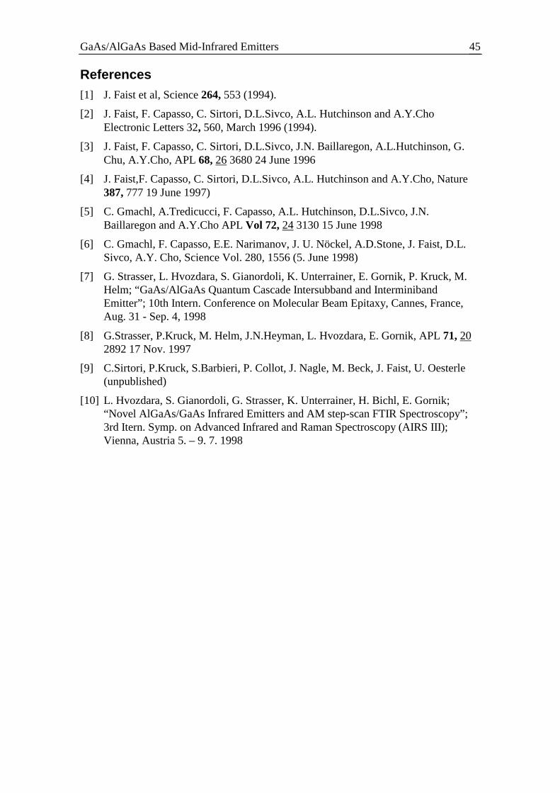
GaAs/AlGaAs Based Mid-Infrared Emitters 45
References[1] J. Faist et al, Science 264, 553 (1994).
[2] J. Faist, F. Capasso, C. Sirtori, D.L.Sivco, A.L. Hutchinson and A.Y.ChoElectronic Letters 32, 560, March 1996 (1994).
[3] J. Faist, F. Capasso, C. Sirtori, D.L.Sivco, J.N. Baillaregon, A.L.Hutchinson, G.Chu, A.Y.Cho, APL 68, 26 3680 24 June 1996
[4] J. Faist,F. Capasso, C. Sirtori, D.L.Sivco, A.L. Hutchinson and A.Y.Cho, Nature387, 777 19 June 1997)
[5] C. Gmachl, A.Tredicucci, F. Capasso, A.L. Hutchinson, D.L.Sivco, J.N.Baillaregon and A.Y.Cho APL Vol 72, 24 3130 15 June 1998
[6] C. Gmachl, F. Capasso, E.E. Narimanov, J. U. Nöckel, A.D.Stone, J. Faist, D.L.Sivco, A.Y. Cho, Science Vol. 280, 1556 (5. June 1998)
[7] G. Strasser, L. Hvozdara, S. Gianordoli, K. Unterrainer, E. Gornik, P. Kruck, M.Helm; “GaAs/AlGaAs Quantum Cascade Intersubband and InterminibandEmitter”; 10th Intern. Conference on Molecular Beam Epitaxy, Cannes, France,Aug. 31 - Sep. 4, 1998
[8] G.Strasser, P.Kruck, M. Helm, J.N.Heyman, L. Hvozdara, E. Gornik, APL 71, 202892 17 Nov. 1997
[9] C.Sirtori, P.Kruck, S.Barbieri, P. Collot, J. Nagle, M. Beck, J. Faist, U. Oesterle(unpublished)
[10] L. Hvozdara, S. Gianordoli, G. Strasser, K. Unterrainer, H. Bichl, E. Gornik;“Novel AlGaAs/GaAs Infrared Emitters and AM step-scan FTIR Spectroscopy”;3rd Itern. Symp. on Advanced Infrared and Raman Spectroscopy (AIRS III);Vienna, Austria 5. – 9. 7. 1998

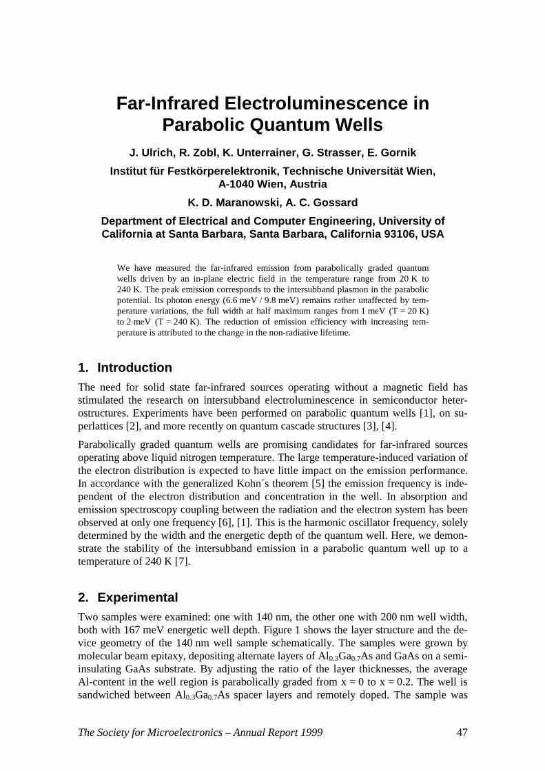
The Society for Microelectronics – Annual Report 1999 47
Far-Infrared Electroluminescence inParabolic Quantum Wells
J. Ulrich, R. Zobl, K. Unterrainer, G. Strasser, E. Gornik
Institut für Festkörperelektronik, Technische Universität Wien,A-1040 Wien, Austria
K. D. Maranowski, A. C. Gossard
Department of Electrical and Computer Engineering, University ofCalifornia at Santa Barbara, Santa Barbara, California 93106, USA
We have measured the far-infrared emission from parabolically graded quantumwells driven by an in-plane electric field in the temperature range from 20 K to240 K. The peak emission corresponds to the intersubband plasmon in the parabolicpotential. Its photon energy (6.6 meV / 9.8 meV) remains rather unaffected by tem-perature variations, the full width at half maximum ranges from 1 meV (T = 20 K)to 2 meV (T = 240 K). The reduction of emission efficiency with increasing tem-perature is attributed to the change in the non-radiative lifetime.
1. IntroductionThe need for solid state far-infrared sources operating without a magnetic field hasstimulated the research on intersubband electroluminescence in semiconductor heter-ostructures. Experiments have been performed on parabolic quantum wells [1], on su-perlattices [2], and more recently on quantum cascade structures [3], [4].
Parabolically graded quantum wells are promising candidates for far-infrared sourcesoperating above liquid nitrogen temperature. The large temperature-induced variation ofthe electron distribution is expected to have little impact on the emission performance.In accordance with the generalized Kohn´s theorem [5] the emission frequency is inde-pendent of the electron distribution and concentration in the well. In absorption andemission spectroscopy coupling between the radiation and the electron system has beenobserved at only one frequency [6], [1]. This is the harmonic oscillator frequency, solelydetermined by the width and the energetic depth of the quantum well. Here, we demon-strate the stability of the intersubband emission in a parabolic quantum well up to atemperature of 240 K [7].
2. ExperimentalTwo samples were examined: one with 140 nm, the other one with 200 nm well width,both with 167 meV energetic well depth. Figure 1 shows the layer structure and the de-vice geometry of the 140 nm well sample schematically. The samples were grown bymolecular beam epitaxy, depositing alternate layers of Al0.3Ga0.7As and GaAs on a semi-insulating GaAs substrate. By adjusting the ratio of the layer thicknesses, the averageAl-content in the well region is parabolically graded from x = 0 to x = 0.2. The well issandwiched between Al0.3Ga0.7As spacer layers and remotely doped. The sample was
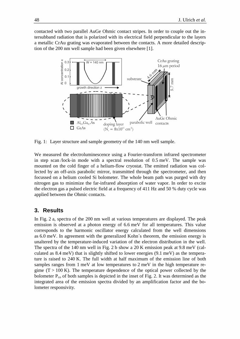
48 J. Ulrich et al.
contacted with two parallel AuGe Ohmic contact stripes. In order to couple out the in-tersubband radiation that is polarized with its electrical field perpendicular to the layersa metallic CrAu grating was evaporated between the contacts. A more detailed descrip-tion of the 200 nm well sample had been given elsewhere [1].
Fig. 1: Layer structure and sample geometry of the 140 nm well sample.
We measured the electroluminescence using a Fourier-transform infrared spectrometerin step scan /lock-in mode with a spectral resolution of 0.5 meV. The sample wasmounted on the cold finger of a helium-flow cryostat. The emitted radiation was col-lected by an off-axis parabolic mirror, transmitted through the spectrometer, and thenfocussed on a helium cooled Si bolometer. The whole beam path was purged with drynitrogen gas to minimize the far-infrared absorption of water vapor. In order to excitethe electron gas a pulsed electric field at a frequency of 411 Hz and 50 % duty cycle wasapplied between the Ohmic contacts.
3. ResultsIn Fig. 2 a, spectra of the 200 nm well at various temperatures are displayed. The peakemission is observed at a photon energy of 6.6 meV for all temperatures. This valuecorresponds to the harmonic oscillator energy calculated from the well dimensionsas 6.0 meV. In agreement with the generalized Kohn´s theorem, the emission energy isunaltered by the temperature-induced variation of the electron distribution in the well.The spectra of the 140 nm well in Fig. 2 b show a 20 K emission peak at 9.8 meV (cal-culated as 8.4 meV) that is slightly shifted to lower energies (9.1 meV) as the tempera-ture is raised to 240 K. The full width at half maximum of the emission line of bothsamples ranges from 1 meV at low temperatures to 2 meV in the high temperature re-gime (T > 100 K). The temperature dependence of the optical power collected by thebolometer Pco of both samples is depicted in the inset of Fig. 2. It was determined as theintegrated area of the emission spectra divided by an amplification factor and the bo-lometer responsivity.
Far-Infrared Electroluminescence in Parabolic Quantum Wells 49
Fig. 2: Emission spectra of the two samples for various temperatures as indicated. Theinset shows the dependence of the collected optical power Pco on the inversetemperature 1/T.
The collected optical power Pco is assumed to depend on the electrical input power Pel
and on the ratio of non-radiative lifetime τnr and radiative lifetime τr (in case of τr >> τnr)like
P Pco elnr
r
∝ττ .
The proportionality between the collected optical power Pco and the electrical inputpower Pel has been confirmed up to ~70 mW, above which saturation occurs. The differ-ence in the optical power Pco between the two samples can be qualitatively understoodby looking at the radiative lifetime τr. It was calculated in the model of a classical elec-tron oscillator as 59 µs for the 140 nm well and 130 µs for the 200 nm well. With thesimplifying assumption of similar non-radiative lifetimes, grating-coupler efficienciesand excitation efficiencies, one would expect the optical power Pco of the 140 nm wellsample to be approximately twice the one of the 200 nm well sample at comparableelectrical input powers Pel.
The decrease of (collected) optical power is induced by a thermally activated process.The solid lines in the inset of Fig. 2 are fits of the inverse sum of two exponential func-tions in 1/T yielding activation energies of E1 = 34 meV, E2 = 0.8 meV for the 140 nmwell sample and E1 = 41 meV, E2 = 2.2 meV for the 200 nm well sample. The higherenergy E1 is probably the activation barrier for the emission of optical phonons. Theintersubband transition rate 1/ τnr shows a similar behavior of thermal activation, as de-
50 J. Ulrich et al.
scribed by Heyman et al. [8]. We may deduce that the temperature dependence of theoptical power is governed by the non-radiative lifetime τnr. At temperatures above~100 K, the emission of optical phonons limits the optical power.
4. ConclusionWe have demonstrated electrically driven far-infrared emission of parabolic quantumwells up to a temperature of 240 K. At high temperatures, the thermal energy kBT ex-ceeds the photon energy by a factor greater than two. Despite of the large temperaturerelated shift of the electron distribution, we observe single frequency emission, and theimpact of high temperatures on the frequency and the line shape is small. The emissionefficiency is limited by the temperature dependent decrease of intersubband lifetime.
AcknowledgementsThis work has been supported by the Austrian Science Foundation (START Y47, Witt-genstein Award), by the EU-TMR Program (INTERACT), and by a QUEST grant.
References[1] K. D. Maranowski, A. C. Gossard, K. Unterrainer, E. Gornik: “Far infrared
emission from parabolically graded quantum wells”, Appl. Phys. Lett., Vol. 69, No.23, p. 3522 - 3524, (1996)
[2] M. Helm, P. England, E. Colas, F. DeRosa, S. J. Allen, Jr.: “Observation of grating-induced intersubband emission from GaAs/AlGaAs superlattices”, Appl. Phys.Lett., Vol. 53, No. 18, p. 1714 – 1716, (1988).
[3] B. Xu, Q. Hu, M. R. Melloch: “Electrically pumped tunable terahertz emitter basedon intersubband transition”, Appl. Phys. Lett., Vol. 71, No. 4, p. 440 – 442, (1997).
[4] M. Rochat, J. Faist, M. Beck, U. Oesterle, M. Ilegems: “Far-infrared (λ = 88 µm)electroluminescence in a quantum cascade structure”, Appl. Phys. Lett., Vol. 73,No. 25, p. 3724 – 3726, (1998).
[5] L. Brey, N. F. Johnson, B. I. Halperin: “Optical and magneto-optical absorption inparabolic quantum wells”, Phys. Rev. B, Vol. 40, No.15, p. 10647 – 10649, (1989).
[6] A. Wixforth, M. Kaloudis, C. Rocke, K. Ensslin, M. Sundaram, J. H. English, A. C.Gossard: “Dynamic response of parabolically confined electron systems”,Semicond. Sci. Technol., Vol 9, p. 215 – 240, (1994).
[7] J. Ulrich, R. Zobl, K. Unterrainer, G. Strasser, E. Gornik, K. D. Maranowski, A. C.Gossard: “Temperature dependence of far-infrared electroluminescence in parabolicquantum wells”, submitted to Appl. Phys. Lett.
[8] J. N. Heyman, K. Unterrainer, C. Craig, B. Galdrikian, M. S. Sherwin, K.Campman, P. F. Hopkins, A. C. Gossard: “Temperature and intensity dependenceof intersubband relaxation rates from photovoltage and absorption”, Phys. Rev.Lett., Vol. 74, No. 14, p. 2682 –2685, (1995).
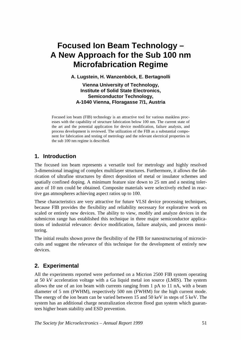
The Society for Microelectronics – Annual Report 1999 51
Focused Ion Beam Technology –A New Approach for the Sub 100 nm
Microfabrication RegimeA. Lugstein, H. Wanzenböck, E. Bertagnolli
Vienna University of Technology,Institute of Solid State Electronics,
Semiconductor Technology,A-1040 Vienna, Floragasse 7/1, Austria
Focused ion beam (FIB) technology is an attractive tool for various maskless proc-esses with the capability of structure fabrication below 100 nm. The current state ofthe art and the potential application for device modification, failure analysis, andprocess development is reviewed. The utilization of the FIB as a substantial compo-nent for fabrication and testing of metrology and the relevant electrical properties inthe sub 100 nm regime is described.
1. IntroductionThe focused ion beam represents a versatile tool for metrology and highly resolved3-dimensional imaging of complex multilayer structures. Furthermore, it allows the fab-rication of ultrafine structures by direct deposition of metal or insulator schemes andspatially confined doping. A minimum feature size down to 25 nm and a nesting toler-ance of 10 nm could be obtained. Composite materials were selectively etched in reac-tive gas atmospheres achieving aspect ratios up to 100.
These characteristics are very attractive for future VLSI device processing techniques,because FIB provides the flexibility and reliability necessary for explorative work onscaled or entirely new devices. The ability to view, modify and analyze devices in thesubmicron range has established this technique in three major semiconductor applica-tions of industrial relevance: device modification, failure analysis, and process moni-toring.
The initial results shown prove the flexibility of the FIB for nanostructuring of microcir-cuits and suggest the relevance of this technique for the development of entirely newdevices.
2. ExperimentalAll the experiments reported were performed on a Micrion 2500 FIB system operatingat 50 kV acceleration voltage with a Ga liquid metal ion source (LMIS). The systemallows the use of an ion beam with currents ranging from 1 pA to 11 nA, with a beamdiameter of 5 nm (FWHM), respectively 500 nm (FWHM) for the high current mode.The energy of the ion beam can be varied between 15 and 50 keV in steps of 5 keV. Thesystem has an additional charge neutralization electron flood gun system which guaran-tees higher beam stability and ESD prevention.
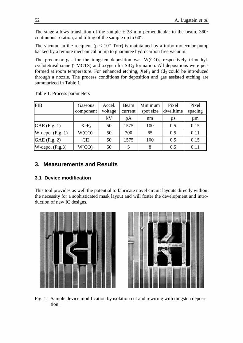
52 A. Lugstein et al.
The stage allows translation of the sample ± 38 mm perpendicular to the beam, 360°continuous rotation, and tilting of the sample up to 60°.
The vacuum in the recipient (p < 10-7 Torr) is maintained by a turbo molecular pumpbacked by a remote mechanical pump to guarantee hydrocarbon free vacuum.
The precursor gas for the tungsten deposition was W(CO)6 respectively trimethyl-cyclotetrasiloxane (TMCTS) and oxygen for SiO2 formation. All depositions were per-formed at room temperature. For enhanced etching, XeF2 and Cl2 could be introducedthrough a nozzle. The process conditions for deposition and gas assisted etching aresummarized in Table 1.
Table 1: Process parameters
FIB Gaseouscomponent
Accel.voltage
Beamcurrent
Minimumspot size
Pixeldwelltime
Pixelspacing
kV pA nm µs µm
GAE (Fig. 1) XeF2 50 1575 100 0.5 0.15
W-depo. (Fig. 1) W(CO)6 50 700 65 0.5 0.11
GAE (Fig. 2) Cl2 50 1575 100 0.5 0.15
W-depo. (Fig.3) W(CO)6 50 5 8 0.5 0.11
3. Measurements and Results
3.1 Device modification
This tool provides as well the potential to fabricate novel circuit layouts directly withoutthe necessity for a sophisticated mask layout and will foster the development and intro-duction of new IC designs.
Fig. 1: Sample device modification by isolation cut and rewiring with tungsten deposi-tion.
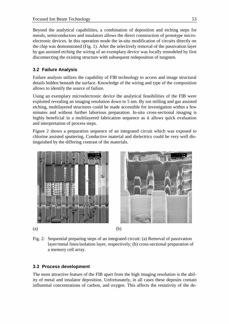
Focused Ion Beam Technology 53
Beyond the analytical capabilities, a combination of deposition and etching steps formetals, semiconductors and insulators allows the direct construction of prototype micro-electronic devices. In this operation mode the in-situ modification of circuits directly onthe chip was demonstrated (Fig. 1). After the selectively removal of the passivation layerby gas assisted etching the wiring of an exemplary device was locally remodeled by firstdisconnecting the existing structure with subsequent redeposition of tungsten.
3.2 Failure Analysis
Failure analysis utilizes the capability of FIB technology to access and image structuraldetails hidden beneath the surface. Knowledge of the wiring and type of the compositionallows to identify the source of failure.
Using an exemplary microelectronic device the analytical feasibilities of the FIB wereexploited revealing an imaging resolution down to 5 nm. By ion milling and gas assistedetching, multilayered structures could be made accessible for investigation within a fewminutes and without further laborious preparation. In-situ cross-sectional imaging ishighly beneficial in a multilayered fabrication sequence as it allows quick evaluationand interpretation of process steps.
Figure 2 shows a preparation sequence of an integrated circuit which was exposed tochlorine assisted sputtering. Conductive material and dielectrics could be very well dis-tinguished by the differing contrast of the materials.
(a) (b)
Fig. 2: Sequential preparing steps of an integrated circuit: (a) Removal of passivationlayer/metal lines/isolation layer, respectively; (b) cross-sectional preparation ofa memory cell array.
3.3 Process development
The most attractive feature of the FIB apart from the high imaging resolution is the abil-ity of metal and insulator deposition. Unfortunately, in all cases these deposits containinfluential concentrations of carbon, and oxygen. This affects the resistivity of the de-
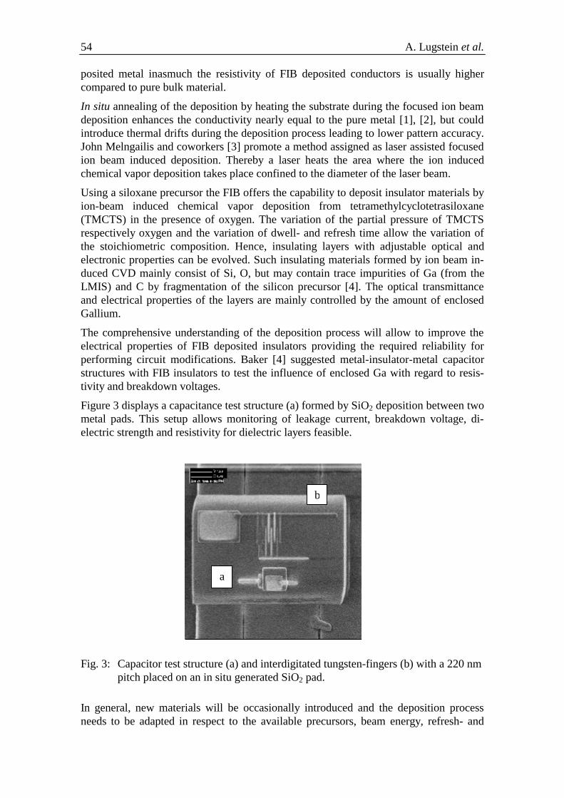
54 A. Lugstein et al.
posited metal inasmuch the resistivity of FIB deposited conductors is usually highercompared to pure bulk material.
In situ annealing of the deposition by heating the substrate during the focused ion beamdeposition enhances the conductivity nearly equal to the pure metal [1], [2], but couldintroduce thermal drifts during the deposition process leading to lower pattern accuracy.John Melngailis and coworkers [3] promote a method assigned as laser assisted focusedion beam induced deposition. Thereby a laser heats the area where the ion inducedchemical vapor deposition takes place confined to the diameter of the laser beam.
Using a siloxane precursor the FIB offers the capability to deposit insulator materials byion-beam induced chemical vapor deposition from tetramethylcyclotetrasiloxane(TMCTS) in the presence of oxygen. The variation of the partial pressure of TMCTSrespectively oxygen and the variation of dwell- and refresh time allow the variation ofthe stoichiometric composition. Hence, insulating layers with adjustable optical andelectronic properties can be evolved. Such insulating materials formed by ion beam in-duced CVD mainly consist of Si, O, but may contain trace impurities of Ga (from theLMIS) and C by fragmentation of the silicon precursor [4]. The optical transmittanceand electrical properties of the layers are mainly controlled by the amount of enclosedGallium.
The comprehensive understanding of the deposition process will allow to improve theelectrical properties of FIB deposited insulators providing the required reliability forperforming circuit modifications. Baker [4] suggested metal-insulator-metal capacitorstructures with FIB insulators to test the influence of enclosed Ga with regard to resis-tivity and breakdown voltages.
Figure 3 displays a capacitance test structure (a) formed by SiO2 deposition between twometal pads. This setup allows monitoring of leakage current, breakdown voltage, di-electric strength and resistivity for dielectric layers feasible.
Fig. 3: Capacitor test structure (a) and interdigitated tungsten-fingers (b) with a 220 nmpitch placed on an in situ generated SiO2 pad.
In general, new materials will be occasionally introduced and the deposition processneeds to be adapted in respect to the available precursors, beam energy, refresh- and
a
b
Focused Ion Beam Technology 55
dwelltime etc. to achieve the desired resistance, dielectric strength, contact resistanceand interconnect properties (ohmic or rectifying).
The installation of routine test vehicles is projected for systematic investigation of themorphological and electrical features obtained for specific deposition parameters. Thedeposition process was found to strongly affect the line width, nesting tolerance, contacthole sizes, etc., and yield of structures. Unified test vehicles provide a suitable mean forgaining a thorough understanding of the complex deposition mechanism.
First test structures (Fig. 3) fabricated by FIB deposition were interdigitated fingers witha 220 nm pitch (b) and metal-insulator-metal capacitor structure (a) to determine con-ductor to conductor shorts, surface and interfacial leakage currents respectively the di-electric strength of the SiO2 layer. The highest performance in resolution and patteringachievable was 5 nm respectively 30 nm.
3.4 Shallow implantation
Recent applications of FIB for semiconductor devices focus on an optimized MOSFET(FIBMOS) using the localized beam to fabricate a unique, laterally tailored doping pro-file along the channel. The arrangement of Ga-LMIS in combination with the highresolution ion column and adjustable beam energy in the range from 50 keV to 15 keVallows generating a strategically placed ultrashallow doping profile with tolerable crys-tal distortion. Former investigations [5] confirmed that the output resistance improves,detrimental hot electron effects diminish and threshold voltage stabilizes as channellength is reduced, which in general leads to significantly better device performance.
4. ConclusionConcluding the presented material illustrates the potential of FIB for metrology andhighly resolved 3-dimensional imaging of complex multilayer structures. Spatially con-fined doping and deposition of metal as well as insulating layers was demonstrated inspatially confined areas in the nm range. Concluding, FIB is a prospective tool for theimprovement of high-frequency devices as well as fabrication of entirely new circuits.
References[1] P.G. Blauner, J.S. Ro, Y. Butt, C.V. Thompson, and J. Melngailis, J. Vac. Sci.
Technol. B. 7, 1816 (1998)
[2] A.D. Della Ratta, J. Melngailis, and C.V. Thompson, J. Vac. Sci. Technol. B. 11,2195 (1993)
[3] J. Funatsu, C. V. Thompson, and J. Melngailis, J. Vac. Sci. Technol. B. 14 (1)(1996)
[4] J.R. Baker, “Focused Ion Beam Insulator Deposition” Proc. 21st Internat. Symp.For testing and Failure Analysis, 6-10 Nov. 1995 Santa Clara, CA, pp. 43-47
[5] C.C. Shen, J. Murguia, N. Goldsman, M. Peckerar, IEEE Transactions on electronDevices, Vol. 45, No. 2, (1998)

The Society for Microelectronics – Annual Report 1999 57
Internal Characterization of IGBTs Using theBackside Laserprobing Technique
C. Fürböck, M. Litzenberger, E. Gornik
Institute for Solid State Electronics & Center of MicrostructureResearch (MISZ),TU Wien, A-1040 Vienna, Austria
R. Thalhammer,G. Wachutka
Physics of Electrotechnology, Munich University of Technology,Munich, Germany
N. Seliger
Siemens AG, Corporate Technology, Munich, Germany
This work presents the time-resolved measurement of charge carrier concentrationand temperature profiles in IGBTs by Backside Laserprobing. Calibrated numericaldevice simulation is employed for investigating the effects of the sample preparationon the device under test and for supporting the interpretation of the experimental re-sults.
1. IntroductionThe high operating temperature due to extensive heat dissipation has become a severeand critical issue in the optimization of modern power semiconductor devices as theblocking voltage and forward current are steadily increasing [1]. Time-resolved meas-urements of carrier concentration and temperature during dynamic device operation pro-vide valuable information for the verification and calibration of the electrothermal mod-els [2] implemented in device simulation tools. In this paper we present the thermalcharacterization of Insulated Gate Bipolar Transistors (IGBTs) during transient switch-ing under shorted load conditions.
The interpretation of the results is supported by calibrated numerical device simulation.Moreover, the relevance of effects on the measurement results introduced by the samplepreparation are studied by multi-cell simulation.
2. Backside LaserprobingThe Backside Laserprobing technique makes use of the dependence of the refractiveindex of silicon on temperature (thermo-optical effect [3]) and on carrier concentration(plasma-optical effect [4]). The modulation of the refractive index is measured by de-tecting the phase shift of an infrared laser beam (λ = 1.3µm). The laser beam propagatesin vertical direction and is reflected at the top metallization layer (as illustrated in Fig.1). Thereby, its phase is shifted by
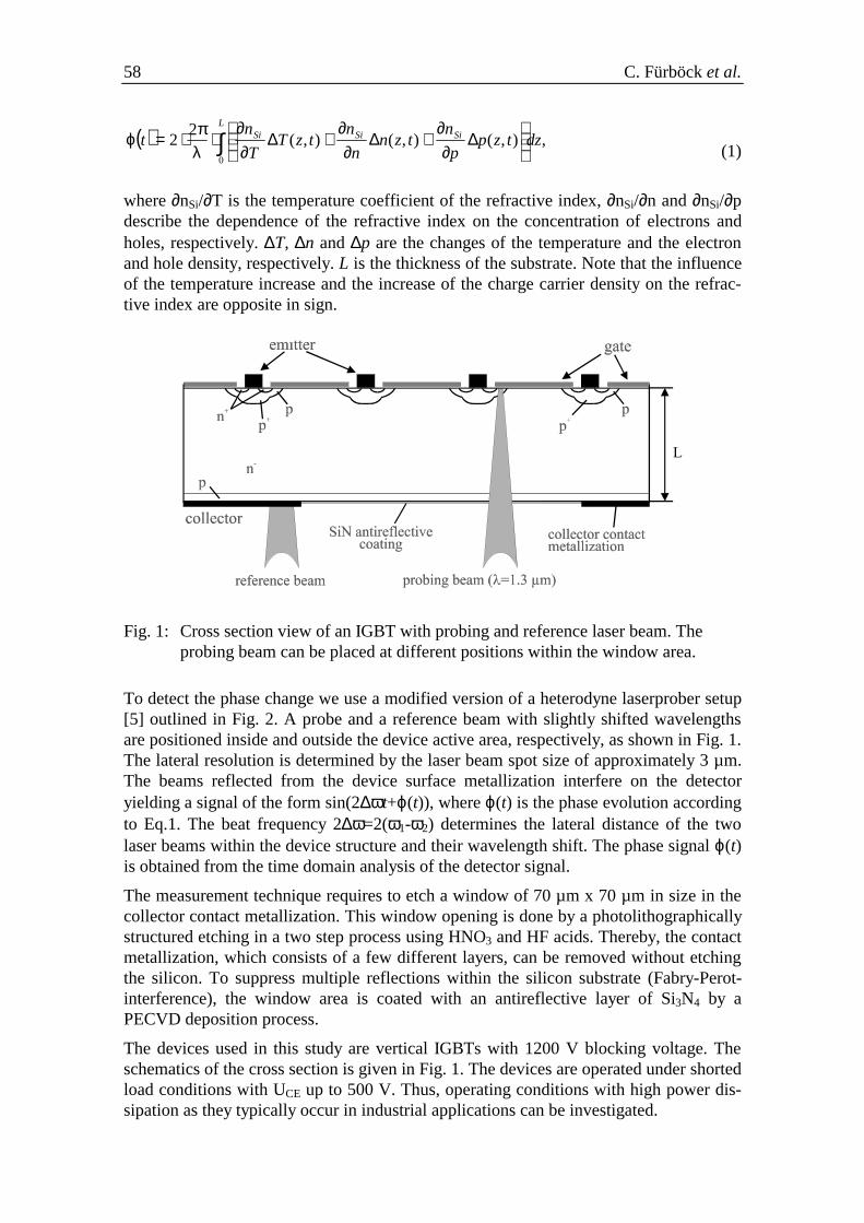
58 C. Fürböck et al.
( ) ∫
∆
∂∂
+∆∂
∂+∆
∂∂
⋅λπ⋅=ϕ
LSiSiSi dztzpp
ntzn
n
ntzT
T
nt
0
,),(),(),(2
2(1)
where ∂nSi/∂T is the temperature coefficient of the refractive index, ∂nSi/∂n and ∂nSi/∂pdescribe the dependence of the refractive index on the concentration of electrons andholes, respectively. ∆T, ∆n and ∆p are the changes of the temperature and the electronand hole density, respectively. L is the thickness of the substrate. Note that the influenceof the temperature increase and the increase of the charge carrier density on the refrac-tive index are opposite in sign.
Fig. 1: Cross section view of an IGBT with probing and reference laser beam. Theprobing beam can be placed at different positions within the window area.
To detect the phase change we use a modified version of a heterodyne laserprober setup[5] outlined in Fig. 2. A probe and a reference beam with slightly shifted wavelengthsare positioned inside and outside the device active area, respectively, as shown in Fig. 1.The lateral resolution is determined by the laser beam spot size of approximately 3 µm.The beams reflected from the device surface metallization interfere on the detectoryielding a signal of the form sin(2∆ωt+ϕ(t)), where ϕ(t) is the phase evolution accordingto Eq.1. The beat frequency 2∆ω=2(ω1-ω2) determines the lateral distance of the twolaser beams within the device structure and their wavelength shift. The phase signal ϕ(t)is obtained from the time domain analysis of the detector signal.
The measurement technique requires to etch a window of 70 µm x 70 µm in size in thecollector contact metallization. This window opening is done by a photolithographicallystructured etching in a two step process using HNO3 and HF acids. Thereby, the contactmetallization, which consists of a few different layers, can be removed without etchingthe silicon. To suppress multiple reflections within the silicon substrate (Fabry-Perot-interference), the window area is coated with an antireflective layer of Si3N4 by aPECVD deposition process.
The devices used in this study are vertical IGBTs with 1200 V blocking voltage. Theschematics of the cross section is given in Fig. 1. The devices are operated under shortedload conditions with UCE up to 500 V. Thus, operating conditions with high power dis-sipation as they typically occur in industrial applications can be investigated.
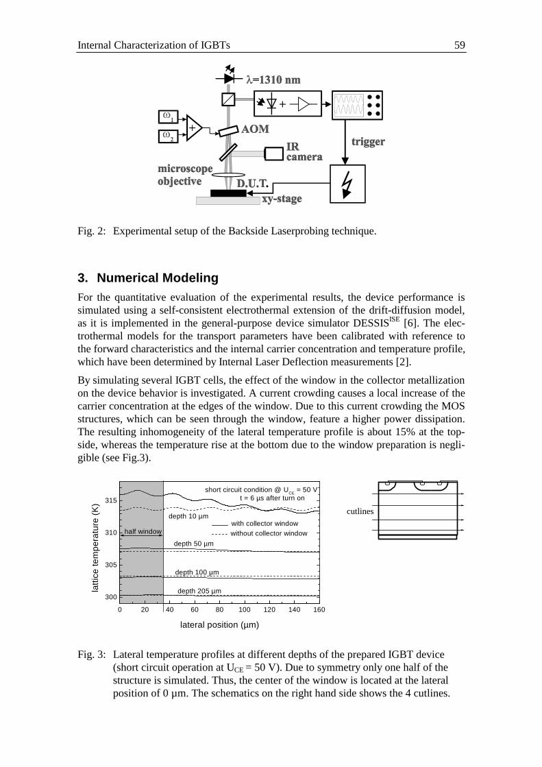
Internal Characterization of IGBTs 59
Fig. 2: Experimental setup of the Backside Laserprobing technique.
3. Numerical ModelingFor the quantitative evaluation of the experimental results, the device performance issimulated using a self-consistent electrothermal extension of the drift-diffusion model,as it is implemented in the general-purpose device simulator DESSISISE [6]. The elec-trothermal models for the transport parameters have been calibrated with reference tothe forward characteristics and the internal carrier concentration and temperature profile,which have been determined by Internal Laser Deflection measurements [2].
By simulating several IGBT cells, the effect of the window in the collector metallizationon the device behavior is investigated. A current crowding causes a local increase of thecarrier concentration at the edges of the window. Due to this current crowding the MOSstructures, which can be seen through the window, feature a higher power dissipation.The resulting inhomogeneity of the lateral temperature profile is about 15% at the top-side, whereas the temperature rise at the bottom due to the window preparation is negli-gible (see Fig.3).
0 20 40 60 80 100 120 140 160
300
305
310
315
depth 205 µm
depth 100 µm
depth 50 µm
t = 6 µs after turn onshort circuit condition @ U
CE = 50 V
without collector windowwith collector window
depth 10 µm
half window
latti
ce te
mpe
ratu
re (
K)
lateral position (µm)
cutlines
Fig. 3: Lateral temperature profiles at different depths of the prepared IGBT device(short circuit operation at UCE = 50 V). Due to symmetry only one half of thestructure is simulated. Thus, the center of the window is located at the lateralposition of 0 µm. The schematics on the right hand side shows the 4 cutlines.
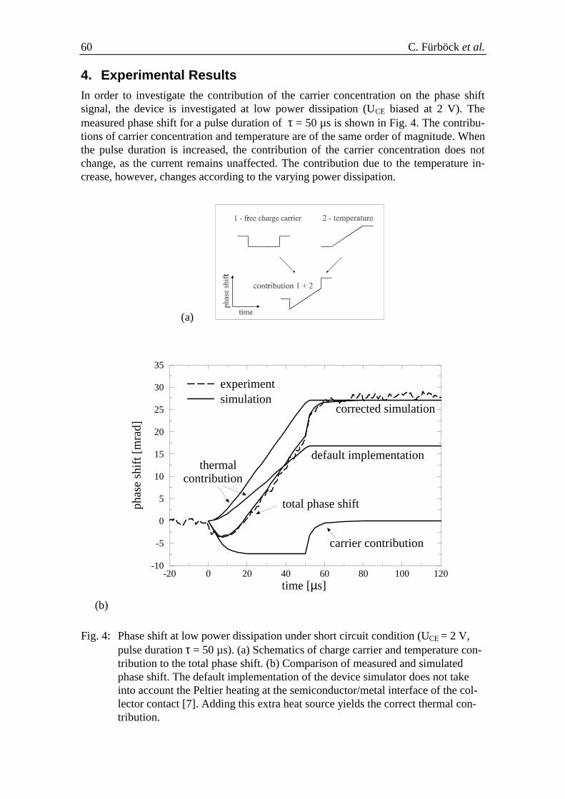
60 C. Fürböck et al.
4. Experimental ResultsIn order to investigate the contribution of the carrier concentration on the phase shiftsignal, the device is investigated at low power dissipation (UCE biased at 2 V). Themeasured phase shift for a pulse duration of τ = 50 µs is shown in Fig. 4. The contribu-tions of carrier concentration and temperature are of the same order of magnitude. Whenthe pulse duration is increased, the contribution of the carrier concentration does notchange, as the current remains unaffected. The contribution due to the temperature in-crease, however, changes according to the varying power dissipation.
(a)
(b)
-20 0 20 40 60 80 100 120time [µs]
-10
-5
0
5
10
15
20
25
30
35
phas
e sh
ift [
mra
d]
experimentsimulation
carrier contribution
thermalcontribution
total phase shift
default implementation
corrected simulation
Fig. 4: Phase shift at low power dissipation under short circuit condition (UCE = 2 V,pulse duration τ = 50 µs). (a) Schematics of charge carrier and temperature con-tribution to the total phase shift. (b) Comparison of measured and simulatedphase shift. The default implementation of the device simulator does not takeinto account the Peltier heating at the semiconductor/metal interface of the col-lector contact [7]. Adding this extra heat source yields the correct thermal con-tribution.
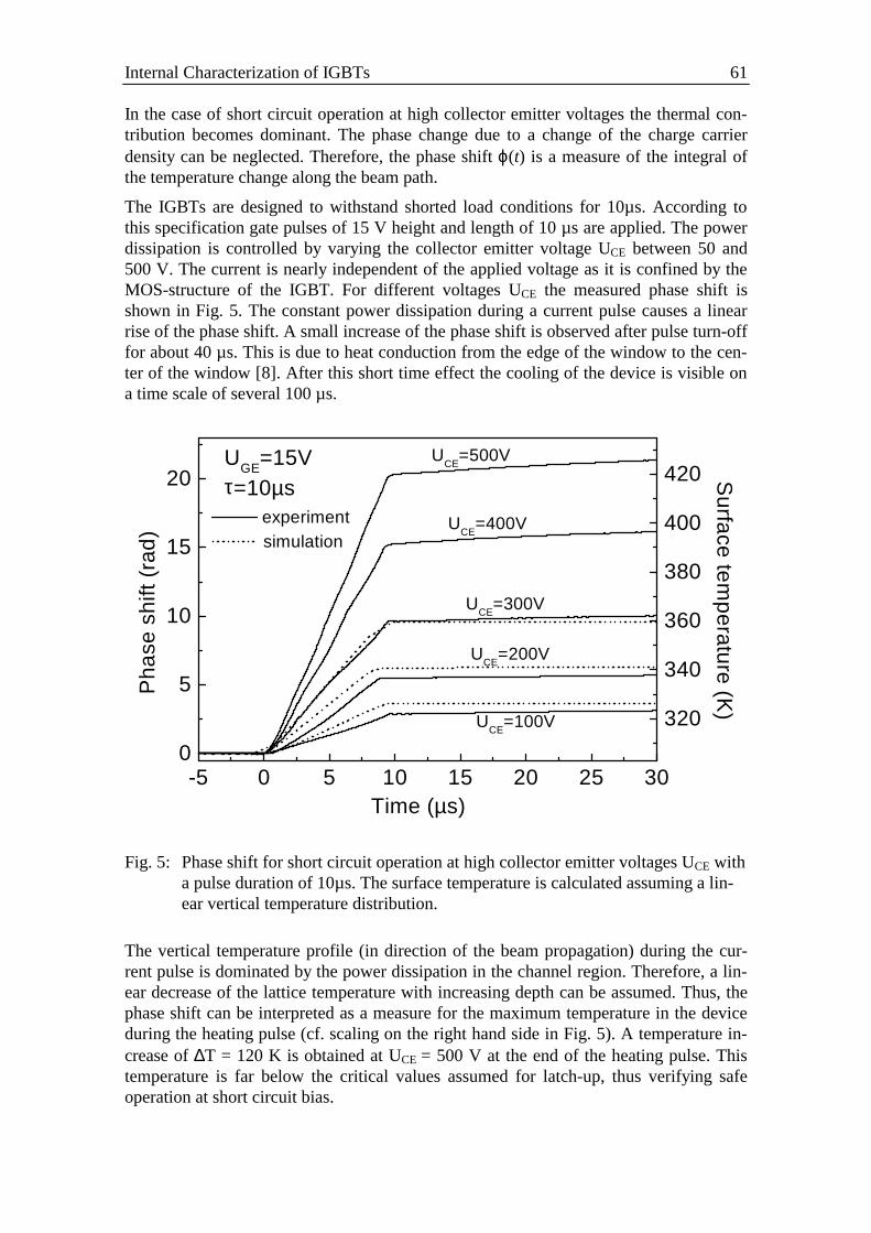
Internal Characterization of IGBTs 61
In the case of short circuit operation at high collector emitter voltages the thermal con-tribution becomes dominant. The phase change due to a change of the charge carrierdensity can be neglected. Therefore, the phase shift ϕ(t) is a measure of the integral ofthe temperature change along the beam path.
The IGBTs are designed to withstand shorted load conditions for 10µs. According tothis specification gate pulses of 15 V height and length of 10 µs are applied. The powerdissipation is controlled by varying the collector emitter voltage UCE between 50 and500 V. The current is nearly independent of the applied voltage as it is confined by theMOS-structure of the IGBT. For different voltages UCE the measured phase shift isshown in Fig. 5. The constant power dissipation during a current pulse causes a linearrise of the phase shift. A small increase of the phase shift is observed after pulse turn-offfor about 40 µs. This is due to heat conduction from the edge of the window to the cen-ter of the window [8]. After this short time effect the cooling of the device is visible ona time scale of several 100 µs.
-5 0 5 10 15 20 25 300
5
10
15
20
experiment
UGE
=15Vτ=10µs
UCE
=400V
UCE
=300V
UCE
=200V
UCE
=100V
UCE
=500V
Pha
se s
hift
(rad
)
Time (µs)
320
340
360
380
400
420 Surfa
ce te
mp
erature (K)
simulation
Fig. 5: Phase shift for short circuit operation at high collector emitter voltages UCE witha pulse duration of 10µs. The surface temperature is calculated assuming a lin-ear vertical temperature distribution.
The vertical temperature profile (in direction of the beam propagation) during the cur-rent pulse is dominated by the power dissipation in the channel region. Therefore, a lin-ear decrease of the lattice temperature with increasing depth can be assumed. Thus, thephase shift can be interpreted as a measure for the maximum temperature in the deviceduring the heating pulse (cf. scaling on the right hand side in Fig. 5). A temperature in-crease of ∆T = 120 K is obtained at UCE = 500 V at the end of the heating pulse. Thistemperature is far below the critical values assumed for latch-up, thus verifying safeoperation at short circuit bias.
62 C. Fürböck et al.
5. ConclusionThe internal transient behavior of vertical IGBTs under short circuit conditions has beenstudied by employing the Backside Laserprobing technique. Charge and temperatureinduced phase signals are analyzed in order to determine the temperature variation in thesurface region. The influence of the preparation of the samples has been investigated byaccurate numerical simulations, which have shown to be indispensable for the correctinterpretation of the experimental results.
AcknowledgementsThis work was partly supported by the “Bundesministerium für Wissenschaft undVerkehr”. The authors would like to thank Dr. G. Deboy (Siemens AG, SemiconductorDivision, Munich) and Dr. G. Sölkner (Siemens AG, Corporate Technology, Munich)for providing the samples and fruitful discussions.
References[1] B.J. Baliga: “Trends in power semiconductor devices”, IEEE Trans. Electron
Devices, Vol. 43(10), 1996, pp. 1717 - 1731.
[2] R. Thalhammer, G. Deboy, E.Knauf, E. Kühbandner, and G. Wachutka:“Calibration of electrothermal power device models using combinedcharacterization techniques”, in Proc. ISPSD, Weimar, Germany, 1997, pp. 181 –184.
[3] H. W. Icenogle, B. C. Platt, and W. L. Wolfe: “Refractive indexes and temperaturecoefficients of germanium and silicon”, Applied Optics, Vol. 15, 1976, pp. 2348 –2351.
[4] R. Soref, and B. Benett: “Electrooptical effects in silicon”, IEEE J. QuantumElectr., Vol. QE-23(1), 1987, pp. 123 – 129.
[5] M. Goldstein, G. Sölkner, and E. Gornik: “Heterodyne interferometer for thedetection of electric and thermal signals in integrated signals through thesubstrate”, Rev.Sci.Instr., Vol. 64(4), 1995, pp. 3009 - 3013.
[6] R. Escoffier, U. Krummbein, E. Lyumkis, B. Polsky, A. Schenk, B. Schmithüsen,C. Steiner, and W. Fichtner: “DESSIS 4.0 Manual”, ISE Integrated SystemsEngineering AG, Zurich, CH (1996).
[7] R. Thalhammer, G. Deboy, W. Keilitz, U. Müller, and G. Wachutka:“Electrothermal effects in Semiconductor Power Devices Analyzed by NumericalSimulation and Internal Laser Deflection Measurement”, in Proc. of ISDRS,Charlottesville, USA, 1995, pp. 51 – 55.
[8] C. Fürböck, R. Thalhammer, M. Litzenberger, N. Seliger, G. Wachutka, and E.Gornik: accepted for publication at ISPSD, Toronto, Canada, 1999.
The Society for Microelectronics – Annual Report 1999 63
Enhanced Energy Resolution in BallisticElectron Emission Microscopy Through
InAs Base LayersR. Heer, J. Smoliner, G. Strasser, and E. Gornik
Institute of Solid State Electronics & Microstructure Research Center,TU Vienna, Floragasse 7, A-1040 Vienna, Austria
Ballistic Electron Emission Spectroscopy (BEES) and Ballistic Electron EmissionMicroscopy (BEEM) offer the unique possibility of probing subsurface quantumstates. To improve the spectroscopic sensitivity, it is important to increase theamount of electrons which are able to penetrate into the sample. In this work weshow that the transmission coefficient and the attenuation length of the base layer canbe enhanced by more than one order of magnitude, if the commonly used thin metalfilm is replaced by a molecular beam epitaxy (MBE) grown InAs layer. At low tem-peratures (T = 100 K), a passivated InAs layer yields an attenuation length in the or-der of 70 nm – 90 nm instead of 5 nm obtained on Au films.
During the last years, scanning tunneling microscopy (STM) and related techniqueshave evolved as powerful tools in the investigation of surfaces [1], [2]. With the intro-duction of ballistic electron emission microscopy/spectroscopy by Kaiser and Bell [3],[4] the unique spatial resolution of the STM has been combined with the possibility oflocal probing the electronic structure of sub-surface interfaces.
In typical BEEM experiments, the ballistic electron current is in the low pA range andthus, the transmission coefficient though the metal base becomes a limiting factor forspectroscopic resolution. If buried structures, such as minibands in superlattices, shall beinvestigated [5], the ballistic electron current through the superlattice will be smaller byat least one order of magnitude than e.g. for an Au-GaAs Schottky diode. In this work,low temperature BEEM studies are carried out on MBE grown InAs-GaAs heterostruc-tures, where a degenerately n-doped InAs layer replaces the commonly used metallicbase. At appropriate growth temperatures (550 °C) a closed and suitable flat InAs layerwas achieved. Due to the large lattice mismatch between InAs and GaAs (7.2 %), suchlayers are strained, but as shown by Ke and coworkers [8] the strain is fully relaxed bydislocations for film thickness above 33 monolayers. InAs carries the unique advantageof a surface accumulation layer. For this reason, insulating surface depletion barrierslike on other semiconductors such as GaAs or silicon do not play a role.
InAs-GaAs heterostructures with InAs film thickness between 160 nm and 300 nm wereinvestigated. Bar-shaped InAs mesas (0.3 mm x 2.5 mm) were defined by photolitho-graphy and using a wet chemical etchant. Then, a In-Sn back contact was alloyed informing gas atmosphere. A second etch process was made to obtain different InAs filmthickness, followed by a polishing and passivation process based on an aqueousP2S5/(NH4)2S solution originally introduced for GaAs [6]. Finally, an In-coated Au-wirewas attached to establish an ohmic contact to the InAs layer. More details on this passi-vation process will be published elsewhere [11]. At room temperature, the internal re-sistance of the InAs samples was too low for reliable BEEM current detection and thus
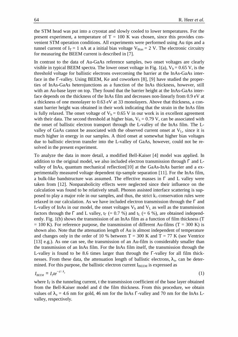
R. Heer et al.64
the STM head was put into a cryostat and slowly cooled to lower temperatures. For thepresent experiment, a temperature of T = 100 K was chosen, since this provides con-venient STM operation conditions. All experiments were performed using Au tips and atunnel current of IT = 1 nA at a initial bias voltage VBias = 2 V. The electronic circuitryfor measuring the BEEM current is described in [7].
In contrast to the data of Au-GaAs reference samples, two onset voltages are clearlyvisible in typical BEEM spectra. The lower onset voltage in Fig. 1(a), Vb = 0.65 V, is thethreshold voltage for ballistic electrons overcoming the barrier at the InAs-GaAs inter-face in the Γ-valley. Using BEEM, Ke and coworkers [8], [9] have studied the proper-ties of InAs-GaAs heterojunctions as a function of the InAs thickness, however, stillwith an Au-base layer on top. They found that the barrier height at the InAs-GaAs inter-face depends on the thickness of the InAs film and decreases non-linearly from 0.9 eV ata thickness of one monolayer to 0.63 eV at 33 monolayers. Above that thickness, a con-stant barrier height was obtained in their work indicating that the strain in the InAs filmis fully relaxed. The onset voltage of Vb = 0.65 V in our work is in excellent agreementwith their data. The second threshold at higher bias, VL = 0.79 V, can be associated withthe onset of ballistic electron transport through the L-valley of the InAs film. The L-valley of GaAs cannot be associated with the observed current onset at VL, since it ismuch higher in energy in our samples. A third onset at somewhat higher bias voltagesdue to ballistic electron transfer into the L-valley of GaAs, however, could not be re-solved in the present experiment.
To analyze the data in more detail, a modified Bell-Kaiser [4] model was applied. Inaddition to the original model, we also included electron transmission through Γ and L-valley of InAs, quantum mechanical reflection[10] at the GaAs-InAs barrier and a ex-perimentally measured voltage dependent tip-sample separation [11]. For the InAs film,a bulk-like bandstructure was assumed. The effective masses in Γ and L valley weretaken from [12]. Nonparabolicity effects were neglected since their influence on thecalculation was found to be relatively small. Phonon assisted interface scattering is sup-posed to play a major role in our samples, and thus, the strict k// conservation rules wererelaxed in our calculation. As we have included electron transmission through the Γ andL-valley of InAs in our model, the onset voltages Vb and VL as well as the transmissionfactors through the Γ and L valley, tΓ (= 0.7 %) and tL (= 6 %), are obtained independ-ently. Fig. 1(b) shows the transmission of an InAs film as a function of film thickness (T= 100 K). For reference purpose, the transmission of different Au-films (T = 300 K) isshown also. Note that the attenuation length of Au is almost independent of temperatureand changes only in the order of 10 % between T = 300 K and T = 77 K (see Ventrice[13] e.g.). As one can see, the transmission of an Au-film is considerably smaller thanthe transmission of an InAs film. For the InAs film itself, the transmission through theL-valley is found to be 8.6 times larger than through the Γ-valley for all film thick-nesses. From these data, the attenuation length of ballistic electrons, λa, can be deter-mined. For this purpose, the ballistic electron current IBEEM is expressed as
IBEEM = ITte− d / λa (1)
where IT is the tunneling current, t the transmission coefficient of the base layer obtainedfrom the Bell-Kaiser model and d the film thickness. From this procedure, we obtainvalues of λa = 4.6 nm for gold, 46 nm for the InAs Γ-valley and 70 nm for the InAs L-valley, respectively.
Enhanced Energy Resolution in Ballistic Electron Emission Microscopy 65
0
0.4
0.8
1.2
1.6
0.5 0.6 0.7 0.8 0.9 1
exp.L
L+
I BE
EM
(pA
)
VBias
(V)
Γ
Vb=0.65 V
VL=0.79 V
Γ
240 nm InAsT=100 K
(a)
-7
-6
-5
-4
-3
-2
-1
0
1
0 1000 2000 3000
AuInAs LlnAs
ln (
t)
d (nm)
Γ
(b)
Fig. 1: (a) Representative BEEM spectrum for a 240 nm InAs layer. (b) Transmissioncoefficients for ballistic electrons through an Au-film (T = 300 K) and the Γ andL-valley of InAs (T = 100 K).
The attenuation lengths in InAs are approximately one order of magnitude larger than inAu and moreover, the attenuation length in the L-valley is approximately 30 % largerthan for the Γ valley. For the Γ valley, the large attenuation length is qualitatively under-stood by low electron-electron scattering rates, due to the low carrier concentration inthe InAs film compared to a metal film. The large transmission coefficient and the largeattenuation length for electrons passing the L-valley of InAs, however, is somewhat sur-prising and needs a more detailed discussion. In our opinion, the process can be ex-plained as follows: To be transmitted ballistically through the InAs L-valley, the elec-tron has to undergo at least two scattering processes. First, the electron has to gain alarge k-vector, necessary to enter the L-valley of InAs which is located at the boundaryof the Brillouin zone in k-space. After the electron has reached the InAs-GaAs interface,a second scattering process is necessary to enable the transfer from the InAs L-valleyinto the Γ-valley of GaAs. Electron transfer into the L-valley of GaAs will only occur athigher energies and was not observed in the present experiment.
The second major advantage of InAs, or in general semiconductor base layers, resultsfrom the low effective mass. Due to the large electron mass difference in Au and GaAs,parallel momentum conservation leads to considerable electron refraction at the Au-GaAs interface. As a consequence, the energetic distribution of the ballistic electroncurrent is inverted beyond the interface and the corresponding energetic resolution isconsiderably decreased. For InAs-GaAs heterostructures, however, this is not the case,since the effective mass in InAs is smaller than in GaAs. Consequently, the energeticdistribution of the ballistic electron current is focussed beyond the InAs-GaAs interfaceand the energetic resolution of the measurement is enhanced.
In summary, we have performed BEEM studies on InAs-GaAs heterostructures, werethe commonly used metal base was replaced by an degenerately doped InAs film. Wehave demonstrated that the BEEM current and the attenuation length of ballistic elec-trons is enhanced by approximately one order of magnitude on this samples. It is foundthat this enhancement is due to lower scattering rates in the Γ-valley of InAs and also toa large contribution of ballistic electrons passing the semiconductor base through theInAs L-valley. This enhancement of the BEEM current is beneficial for all applications,
R. Heer et al.66
where the BEEM signal is expected to be small such as for the investigation of buriedsuperlattices or self assembled quantum dots.
AcknowledgementsThis work was sponsored by Fonds zur Förderung der wissenschaftlichen Forschung(FWF) project No. P11285-PHY and Gesellschaft für Mikroelektronik (GMe).
References[1] G. Binnig, G. Rohrer, Ch. Gerber, E. Weibel, Phys. Rev. Lett. 49, 57 (1982)
[2] G. Binnig, G. Rohrer, Ch. Gerber, E. Weibel, Phys. Rev. Lett. 50, 120 (1983)
[3] W.J. Kaiser and L.D. Bell, Phys. Rev. Lett. 60, 1408 (1988)
[4] L.D. Bell and W.J. Kaiser, Phys. Rev. Lett. 61, 2368 (1988)
[5] C. Eder, J. Smoliner, R. Heer, G. Strasser, E. Gornik, Proc. MSS8, Santa Barbara(1997), Physica E, Vol. 2/1-4, 850 (1998)
[6] J.A. Dagata, W. Tseng, J. Bennet, J. Schneir, H.H. Harry, Appl. Phys. Lett. 59, 52,(1991)
[7] R. Heer, C. Eder, J. Smoliner, E. Gornik, Rev. Sci. Instr. 68, 4488, (1997)
[8] Mao-Iong Ke, D.I. Westwood, C.C. Matthai, B.E. Richardson, R.H. Williams, J.Vac. Sci. Technol. B 14, 2786 (1996)
[9] Mao-Iong Ke, D.I. Westwood, S.Wilks, S.Heghoyan, A.Kestle, C.C.Matthai, B.E.Richardson, R.H. Williams, J. Vac. Sci. Technol. B 13 1684 (1995)
[10] M. Prietsch, Physics Reports 253, 163 (1995)
[11] R. Heer, J. Smoliner, G. Strasser, E. Gornik, to appear in Phys. Rev.B (15 January1999)
[12] The InAs effective masses were obtained through a non-local pseudopotentialcalculation carried out by. P. Vogl, Walter Schottky Institute, Munich. (originalcode by J.R. Chelikowsky, M.L.Cohen see Phys. Rev. B 14, 556 (1976)). All otherdata were taken from Landolt Börnstein, Numerical Data and FunctionalRelationships in Science and Technology, New Series, Vol.17: Physics of GroupIV Elements and III-V compounds; Springer New York (1984)
[13] C.A. Ventrice, V.P. La Bella, G. Ramaswamy, H.P. Yu, L.J. Schowalter, Appl.Surf. Sci. 104/105, 274, (1996)
The Society for Microelectronics – Annual Report 1999 67
Onset of Scattering Induced MinibandTransport
C. Rauch, G. Strasser, and E. GornikInstitut für Festkörperelektronik und Mikrostrukturzentrum der TU Wien,
Technische Universität Wien, Floragasse 7, A-1040 Wien, Austria
A systematic study of electron transport in undoped GaAs/GaAlAs superlattices ispresented. Hot electron spectroscopy is used to measure the superlattice transmit-tance at different bias conditions. The transmittance of a five period superlattice isfound to be independent of the direction of the electric field, while for a superlatticelarger than ten periods, a dependence of the transmission on the electric field direc-tion is observed. The onset of scattering induced miniband transport is clearly evi-dent. From the experimental data a coherence length of 150 nm is derived. The lim-iting mechanism is found to be interface roughness scattering.
1. IntroductionDecreasing the barrier thickness of multiple quantum well structures leads to a strongercoupling between the degenerate eigenstates in the wells and thus to the formation ofsuperlattice minibands. The application of an external electric field parallel to thegrowth axis quantizes the energy continuum associated with the miniband dispersioninto a Stark ladder of discrete energy levels, and transforms the extended Bloch wavesinto strongly localized wave functions. Under strong localization coherence will be re-duced to a few periods and in the limit, to a single quantum well.
Numerous studies of the formation of superlattice minibands have been reported in-cluding transport measurements of biased n-i-n superlattice structures. However, it turnsout that the experimental study of electronic properties of a biased superlattice is hin-dered by the interdependence of the intensity of the current injected and the field presentin the superlattice [1]. At high electric fields the large current densities make the field inthe superlattice non-uniform and causes the formation of high field domains and leads tothermal saturation of miniband transport [2].
In this work we present a study of ballistic transport in nominally undoped GaAs/Ga0.7Al 0.3As superlattices, where the influence of electron-electron and electron-impurity scattering can be neglected. Under flat band conditions the eigenstates of theperiodic structure are expected to be extended over the entire length of the superlattice.We apply the technique of hot electron spectroscopy to measure the positions of theminibands and to investigate the transmission of hot electrons in biased superlattices.
2. ExperimentA three terminal device is used to probe the transmittance of undoped GaAs/GaAlAssuperlattices. An energy tunable electron beam is generated by a tunneling barrier andpasses the superlattice after traversing a thin highly doped n-GaAs base layer and anundoped drift region. The measured collector current reflects the probability of an in-
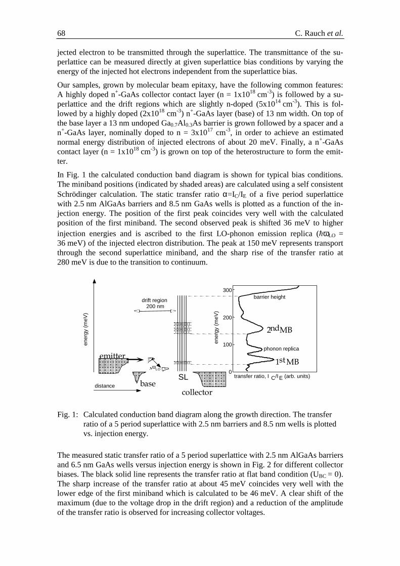
C. Rauch et al.68
jected electron to be transmitted through the superlattice. The transmittance of the su-perlattice can be measured directly at given superlattice bias conditions by varying theenergy of the injected hot electrons independent from the superlattice bias.
Our samples, grown by molecular beam epitaxy, have the following common features:A highly doped n+-GaAs collector contact layer (n = 1x1018 cm-3) is followed by a su-perlattice and the drift regions which are slightly n-doped (5x1014 cm-3). This is fol-lowed by a highly doped (2x1018 cm-3) n+-GaAs layer (base) of 13 nm width. On top ofthe base layer a 13 nm undoped Ga0.7Al 0.3As barrier is grown followed by a spacer and an+-GaAs layer, nominally doped to n = 3x1017 cm-3, in order to achieve an estimatednormal energy distribution of injected electrons of about 20 meV. Finally, a n+-GaAscontact layer (n = 1x1018 cm-3) is grown on top of the heterostructure to form the emit-ter.
In Fig. 1 the calculated conduction band diagram is shown for typical bias conditions.The miniband positions (indicated by shaded areas) are calculated using a self consistentSchrödinger calculation. The static transfer ratio α=IC/IE of a five period superlatticewith 2.5 nm AlGaAs barriers and 8.5 nm GaAs wells is plotted as a function of the in-jection energy. The position of the first peak coincides very well with the calculatedposition of the first miniband. The second observed peak is shifted 36 meV to higherinjection energies and is ascribed to the first LO-phonon emission replica (ωLO =36 meV) of the injected electron distribution. The peak at 150 meV represents transportthrough the second superlattice miniband, and the sharp rise of the transfer ratio at280 meV is due to the transition to continuum.
ωLO
drift region200 nm
SL transfer ratio, I C/I E (arb. units)
ener
gy (
meV
)
ener
gy (
meV
)
300
0
100
200
distance
phonon replica
barrier height
Fig. 1: Calculated conduction band diagram along the growth direction. The transferratio of a 5 period superlattice with 2.5 nm barriers and 8.5 nm wells is plottedvs. injection energy.
The measured static transfer ratio of a 5 period superlattice with 2.5 nm AlGaAs barriersand 6.5 nm GaAs wells versus injection energy is shown in Fig. 2 for different collectorbiases. The black solid line represents the transfer ratio at flat band condition (UBC = 0).The sharp increase of the transfer ratio at about 45 meV coincides very well with thelower edge of the first miniband which is calculated to be 46 meV. A clear shift of themaximum (due to the voltage drop in the drift region) and a reduction of the amplitudeof the transfer ratio is observed for increasing collector voltages.
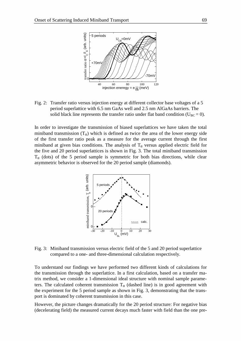
Onset of Scattering Induced Miniband Transport 69
40 60 80 100 120tr
ansf
er r
atio
α=
I C/I
E (
arb.
uni
ts)
injection eneregy = e.UEB
(meV)
5 periods
-70mV0
+70mV
UCB
=0mV
Fig. 2: Transfer ratio versus injection energy at different collector base voltages of a 5period superlattice with 6.5 nm GaAs well and 2.5 nm AlGaAs barriers. Thesolid black line represents the transfer ratio under flat band condition (UBC = 0).
In order to investigate the transmission of biased superlattices we have taken the totalminiband transmission (Tα) which is defined as twice the area of the lower energy sideof the first transfer ratio peak as a measure for the average current through the firstminiband at given bias conditions. The analysis of Tα versus applied electric field forthe five and 20 period superlattices is shown in Fig. 3. The total miniband transmissionTα (dots) of the 5 period sample is symmetric for both bias directions, while clearasymmetric behavior is observed for the 20 period sample (diamonds).
-30 -20 -10 0 10 20 30
min
iban
d tr
ansm
issi
on, T α (
arb.
uni
ts)
USL
(mV)
5 periods
20 periods
0
0
calc.
Fig. 3: Miniband transmission versus electric field of the 5 and 20 period superlatticecompared to a one- and three-dimensional calculation respectively.
To understand our findings we have performed two different kinds of calculations forthe transmission through the superlattice. In a first calculation, based on a transfer ma-trix method, we consider a 1-dimensional ideal structure with nominal sample parame-ters. The calculated coherent transmission Tα (dashed line) is in good agreement withthe experiment for the 5 period sample as shown in Fig. 3, demonstrating that the trans-port is dominated by coherent transmission in this case.
However, the picture changes dramatically for the 20 period structure: For negative bias(decelerating field) the measured current decays much faster with field than the one pre-
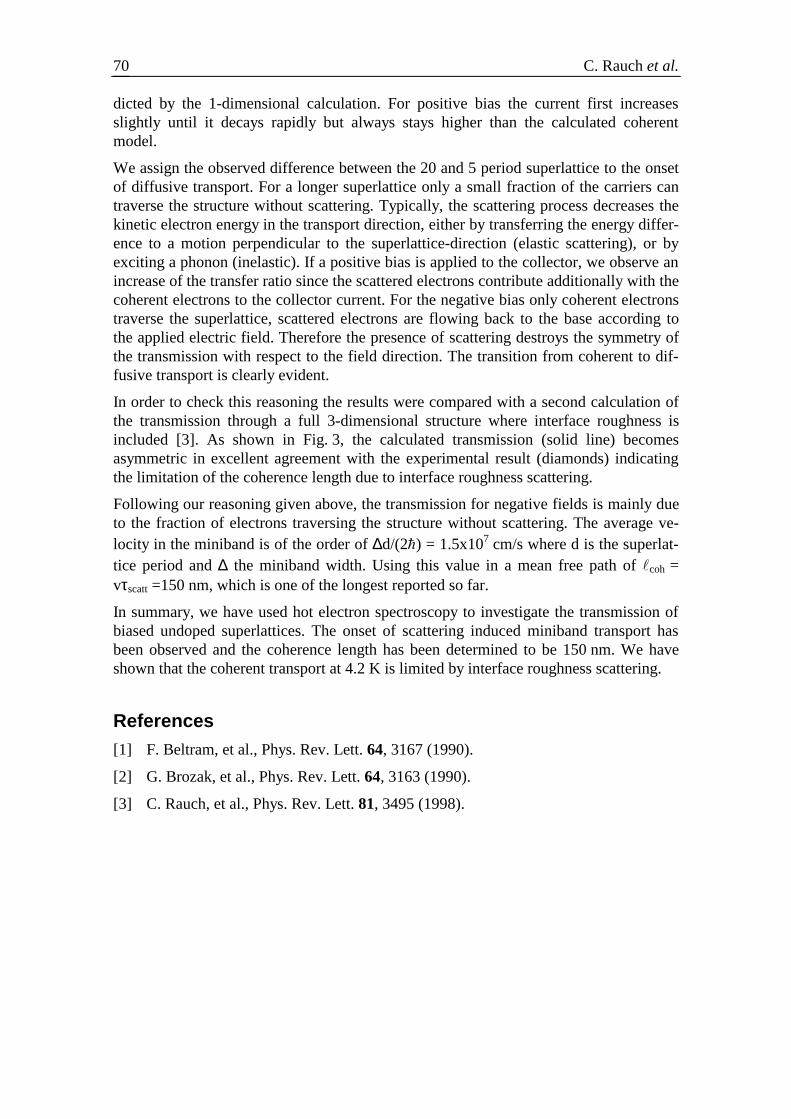
C. Rauch et al.70
dicted by the 1-dimensional calculation. For positive bias the current first increasesslightly until it decays rapidly but always stays higher than the calculated coherentmodel.
We assign the observed difference between the 20 and 5 period superlattice to the onsetof diffusive transport. For a longer superlattice only a small fraction of the carriers cantraverse the structure without scattering. Typically, the scattering process decreases thekinetic electron energy in the transport direction, either by transferring the energy differ-ence to a motion perpendicular to the superlattice-direction (elastic scattering), or byexciting a phonon (inelastic). If a positive bias is applied to the collector, we observe anincrease of the transfer ratio since the scattered electrons contribute additionally with thecoherent electrons to the collector current. For the negative bias only coherent electronstraverse the superlattice, scattered electrons are flowing back to the base according tothe applied electric field. Therefore the presence of scattering destroys the symmetry ofthe transmission with respect to the field direction. The transition from coherent to dif-fusive transport is clearly evident.
In order to check this reasoning the results were compared with a second calculation ofthe transmission through a full 3-dimensional structure where interface roughness isincluded [3]. As shown in Fig. 3, the calculated transmission (solid line) becomesasymmetric in excellent agreement with the experimental result (diamonds) indicatingthe limitation of the coherence length due to interface roughness scattering.
Following our reasoning given above, the transmission for negative fields is mainly dueto the fraction of electrons traversing the structure without scattering. The average ve-locity in the miniband is of the order of ∆d/(2) = 1.5x107 cm/s where d is the superlat-tice period and ∆ the miniband width. Using this value in a mean free path of coh =vτscatt =150 nm, which is one of the longest reported so far.
In summary, we have used hot electron spectroscopy to investigate the transmission ofbiased undoped superlattices. The onset of scattering induced miniband transport hasbeen observed and the coherence length has been determined to be 150 nm. We haveshown that the coherent transport at 4.2 K is limited by interface roughness scattering.
References[1] F. Beltram, et al., Phys. Rev. Lett. 64, 3167 (1990).
[2] G. Brozak, et al., Phys. Rev. Lett. 64, 3163 (1990).
[3] C. Rauch, et al., Phys. Rev. Lett. 81, 3495 (1998).
The Society for Microelectronics – Annual Report 1999 71
Analysis of Single-Mode Grating CoupledTwin Waveguide Laser StructuresN. Finger, P. O. Kellermann, W. Schrenk, and E. Gornik
Institut für Festkörperelektronik, TU-Wien, Floragasse 7, A-1040 Wien
An analysis of semiconductor laser structures with adjustable single-mode emissionbased on a contradirectionally grating coupled twin-waveguide structure consistingof an ITO/low-index dielectric waveguide on top of a corrugated active laserwaveguide is presented. At resonance between the laser mode and the surface modethe grating-coupled radiation losses show a sharp drop with a linewidth comparableto the Fabry-Perot-mode spacing of the laser cavity, thus preferring a single longi-tudinal mode. Intermodal discrimination of up to 20 cm-1 and moderate thresholdgain of ~50 cm-1 can be obtained. Since the resonance wavelength depends on theoptical thickness of the surface waveguide, a simple post-processing adjustment ofthe emission wavelength with a tuning range in excess of ~15 nm can be achieved.
1. IntroductionFor the realization of highly integrated wavelength division multiplexing (WDM)transmitter devices monolithic laser diode arrays are considered as a compact choice dueto their capability of simultaneous transmission of several channels into a single opticalfiber, thus decreasing system size and costs. Efforts on multiwavelength laser diode ar-rays have focussed on DFB [1] and VCSEL laser arrays. Wavelength shift in DFB laserarrays is achieved by changing the grating period of the individual elements which,however, requires a very precise definition of the grating period to achieve a well de-fined emission wavelength. In VCSEL arrays the wavelength shift can be achieved bygenerating a thickness gradient across the wafer during epitaxial growth [2]. Recently afive wavelength laser diode array [3] has been reported which utilizes the surface modeemission (SME) technique [4]. This technique provides the advantage of a simple post-processing adjustment of the emission wavelength of the individual laser diodes byadapting the surface waveguide thickness on top of the structure. A drawback of theSME technique, however, is the relatively low side mode suppression of about 20 dB.The laser structures suggested in this paper combine both the simple post-processingwavelength adjustment of the SME technique and considerable intermodal dis-crimination.
2. Laser StructuresThe laser structures under consideration are based on a GaAs/AlGaAs DH-Laser struc-ture utilizing an InGaAs/GaAs-MQW active region (at λ = 980 nm) embedded in highlyasymmetric cladding layers in order to shift the mode field pattern towards the surface.The n-type cladding layer on top of the GaAs-substrate (refractive index n = 3.523) isformed by Al0.3Ga0.7As (n = 3.333, thickness 1200 nm). The active layer with a thick-ness of 250 nm (n = 3.523) is followed by a typically 300 nm thick p-Al0.2Ga0.8As layer( n =3.393) and a p-GaAs top layer which is 250 nm thick. The top layer is corrugated by
72 N. Finger et al.
a trapezoid shaped grating with the period Λ = 192 nm, duty cycle 0.5, slope angle of70° and a height of 80 nm. The grating is covered with a 120 nm indium tin oxide (ITO,n =1.6 + 0.04i) film which is needed for current injection. The SWG is made of ~200-400 nm SiOx (n = 1.5) below a ~300 nm SiNx layer (n =1.9). This combination of high-index and low-index dielectric is utilized in order to avoid excessive leakage losses intothe high-index substrate.
3. Waveguide ModesSince the WGS is basically a twin waveguide structure, two modes — a laser mode “a”and a surface mode “b” with the propagation constants βa and βb, respectively — exist.The grating causes grating coupled radiation into the substrate thus creating additionallosses. In case of surface mode resonance (SMR), i.e. when the phase matching condi-tion Λπ≈β−β 2ba is satisfied, contradirectional coupling between the mode “a” and
“b” occurs. (Note that 0<ℜ bβ since mode “b” is counterpropagating.) This means that
energy is transferred from the LWG to the SWG and in turn back again. This energytransfer is accompanied by a resonant decrease of the grating coupled radiation loss intothe substrate for both modes. Another benefit of this coupling is the effective increase ofgain which a wave travelling over a certain in the active LWG experiences, since poweris coupled into the SWG where it is transferred into the opposite direction and in turncoupled back into the LWG where it is amplified again.
Fig. 1: Attenuation curves for a WGS with a 120 nm ITO/350 nm SiO/SiN SWG fordifferent SiN thicknesses ranging from 260 to 380 nm. αA and αB are theattenuation constants of the laser mode and the surface mode, respectively.
The analysis used for the calculation of the waveguide properties follows the numericalapproach presented in [5]. It is a coupled mode theory which is based on a rigorous Flo-quet-Bloch analysis of the grating waveguide problem yielding accurate results even forstrong gratings. The governing equations relating the slowly varying amplitudes of thewaves propagating in the LWG and the SWG )(za and )(zb , respectively, are obtained
as ( )bziiaGidzda δ−κ++κ= exp)( 1211 and ( ) biaziidzdb 2221exp κ+δκ= , where the
coupling coefficients κij (i, j = 1, 2) provide information about absorption loss, radiation
Single-Mode Grating Coupled Twin Waveguide Laser Structures 73
loss and coupling between mode “a” and “b”. The influence of gain is described by G ;Λπ−β−β=δ 2ba is the phase mismatch between modes “a” and “b”.
Figure 1 shows the (power) attenuation curves of a WGS with a 250 nm p-Al0.2Ga0.8Aslayer and a 120 nm ITO/350 nm SiO/SiN SWG with SiN-layer thicknesses varying from380 to 260 nm. Since the dispersion of the SWG depends on the SWG thickness theresonance wavelengths range from 990.4 to 975.2 nm. The linewidth of the SMR in-creases from 0.21 nm to 0.53 nm due to increasing leakage losses of the SWG. How-ever, due to the stronger penetration of the SWG field into the grating region a moderateincrease of the mutual coupling coefficient from 27 + 8.4i cm-1 to 45.1 + 21.3i cm-1 isobserved.
4. Finite Length ResonatorsThe finite length resonators are formed by the WGS terminated by as cleaved facets
located at z = ±L/2 (cavity length L) with amplitude reflection coefficients 3.0=ar
and 05.0=br for the LWG and the SWG. The laser structures are basically Fabry-
Perot (FP) cavities with an intrinsic narrow-band wavelength filter favoring to lase justone FP mode coinciding with the resonance wavelength. In order to obtain single modeoperation two requirements must be met: 1) The linewidth of the SMR has to be compa-rable or yet better smaller than the FP mode spacing and 2) a proper matching of theSMR and the FP mode spectrum must be achieved. The former requirement is fulfilledsince both the SMR and the FP mode spacing are in the sub-nm regime. The latter re-quirement, however, needs to be discussed in detail: An effective mode selection onlyoccurs if one of the FP resonances is near the wavelength with minimum losses. If thewavelength of minimum loss is between two FP modes, single mode emission cannot beexpected since both FP modes suffer almost equal losses. The relative position of the FPmodes and the SMR, however, can be adjusted thermally since the FP modes shift witha rate of nm/K067.0=∆∆⋅λ≈∆λ∆ TnnT aaFP , whereas the SMR shifts more slowly
( ( ) nm/K045.0=∆∆⋅+λ≈∆λ∆ TnnnT abares ). This is a consequence of the much
smaller temperature dependence of the effective index of the SWG (nb) than that one ofthe LWG (na). For a cavity length L= 600 µm a temperature deviation of 10 K shifts theFP mode spectrum from one optimum position with respect to the SMR to the next one.Thus in order to avoid mode hopping a temperature stabilization allowing maximumdeviations of ~1 K is necessary.
Figure 2 shows the longitudinal mode spectrum of a laser structure (length 600 µm)with an ITO/SiO/SiN SWG (layer thicknesses 120, 350 and 300 nm; the p-Al0.2Ga0.8Aslayer thickness is 300 nm). Additional losses of 10 cm-1 were assumed for both sub-waveguides. The lowest threshold mode has a mode gain 2G =45.2 cm-1 and a thresholdgain difference of about 14 cm-1 which is suitable for single mode operation with a sidemode suppression of more than 30 dB. A clear resonant decrease of the power radiatedinto the substrate is observed whereas the power emitted via the facets peaks. However,due the resonant increase of optical power in the absorbing ITO layer, also the absorbedpower peaks at the SMR.
74 N. Finger et al.
Fig. 2: Longitudinal mode spectrum (a) and normalized powers (b) for a 600 µm longdevice with an ITO/SiO/SiN SWG. The powers are normalized with respect tothe stimulated emission power.
5. ConclusionWe have suggested a novel design for single-mode laser diodes with adjustable emissionwavelength. The mode selection mechanism is based on a narrow-band suppression ofradiation loss of an active/passive twin-waveguide structure. Intermodal discriminationcan be as high as 20 cm-1 while maintaining relative low threshold gain (~50 cm-1) andmoderate differential output efficiency (~40 %). Simple and precise post-processingwavelength adjustment with a range in excess of ~15 nm is feasible, since changing theSWG thickness yields a shift of the SMR at a rate of 12.0≈∆∆ SWGres dλ .
AcknowledgementsThis work is partly supported by the Volkswagen-Stiftung (Germany).
References[1] L. Davis, M. Mazed, S. Keo, J. Singletary, T. Wang, S. Fourouhar: Proc. SPIE,
vol. 2690, p. 304, 1996.
[2] C.J. Chang-Hasnain, J.P. Harbinson, C.E. Zah, M.W. Maeda, L.T. Florez, N.G.Stoffel, T.P. Lee: IEEE J. Quantum Electron., vol. QE-27, p. 1368, 1991.
[3] A. Golshani, P.O. Kellermann, A. Köck, E. Gornik, L. Korte: “Five-wavelengthsurface emitting laser diode array based on postgrowth wavelength adjustment”,Appl. Phys. Lett., vol. 71, pp. 762-764, 1997.
[4] A. Köck, A. Golshani, R. Hainberger, E. Gornik, L. Korte: “Single-mode andsingle beam emission from surface-emitting laser diodes based on surface modeemission”, Appl. Phys. Lett., vol. 69, pp. 3638-3640, 1996.
[5] N. Finger, E. Gornik: “Analysis of metallized-grating coupled twin-waveguidestructures”, IEEE J. Quantum Electron., submitted for publication, 1998.

The Society for Microelectronics – Annual Report 1999 75
MicroelectronicsTechnology —
Cleanroom Linz

The Society for Microelectronics – Annual Report 1999 77
Microstructure Research: Cleanroom LinzG. Bauer, H. Heinrich, H. Thim, G. Brunthaler
Institut für Halbleiter- und Festkörperphysik,and Institut für Mikroelektronik,
Johannes Kepler Universität Linz, A-4040 Linz, Austria
The GMe supports in Linz the microstructure research in the cleanrooms of the In-stitut für Halbleiter- und Festkörperphysik and the Institut für Mikroelektronik. Inthe field of high frequency devices in 1998 a 0.5 µm MESFET-technology was de-veloped and adapted for the realization of a hot-electron injection field effect tran-sistor. In a collaboration with an Austrian company processing steps for a Si/SiGeheterobipolar transistor were investigated and Si/SiGe MODFET structures werefabricated. The capabilities for nanostructure patterning were expanded by furtherwork on e-beam lithography as well as on scanning force microscopy, where struc-tural widths down to 30 nm could be realized. The optoelectronic activities werepursued for Er-doped Si for light generation in the 1.54 µm wavelength range, and inparticular electroluminescence investigations were carried out at 77 K and 300 K.Furthermore, using II-VI compounds ZnSe/ZnCdSe quantum wires were fabricatedby overgrowth on prepatterned GaAs substrates, and their luminescence was studied,and highly efficient mid-infrared Bragg mirrors were grown using IV-VI heterolay-ers. Semiconductor nanostructures fabricated by self-assembled growth (Si/SiGe,Mn/CdTe and PbSe/PbEuTe) were investigated with respect to their elastic proper-ties, and for the first time a three dimensional ordering could be observed.
1. IntroductionThe funding of the activities in the two cleanrooms at the University of Linz which arejointly used by three groups is of vital importance for our microstructure research ac-tivities. This basic funding allows for investigations which are made possible throughadditional funding coming from the FWF, the OeNB, as well as through cooperationswith industrial groups as listed below.
In the following short presentations an overview is given on the achievements in theyear 1998. The basic equipment which is available in the clean rooms allows for MBEgrowth of Si-based heterostructures, of II-VI and IV-VI heterostructures, as well as forMOCVD growth of III-V compounds like GaAs/GaAlAs and GaAs/GaInAs. Apart fromin-situ and ex-situ structural characterization, lateral patterning is made possible throughequipment like optical, holographic and electron beam lithography. Processing includesalso facilities for the deposition on insulating as well as contact layers.
Consequently, studies related to high frequency electronic and to optoelectronic devicescan be performed which are described in some detail below and which were also pre-sented at the meeting of the GMe held in Hofgastein in March 1999.
For the section on HF-systems, the microelectronics group has performed studies on aKa-band detector InGaAs Schottky diode with high sensitivity for the 35GHz band. Thisdiode is actually used as the receiving part of a Doppler-radar front end, developed bythis group.
78 G. Bauer et al.
HF devices for the lower GHz range are now in the focus of the interest through theirimportance for communication and are important for the Austrian industry as well. Inthe semiconductor physics group in Linz work on the realization of a Si/SiGeC basedheterobipolar transistor is in progress, where the carbon in the base region prevents theoutdiffusion of the boron and thus allows for appreciably higher doping levels than instandard Si/SiGe HBT’s. Si/SiGe based modulation doped field effect transistors werefabricated using MBE grown samples. The complete transistor requires six lithographicsteps, with contact lithography down to 0.5 micrometers and e-beam lithography belowthis size. The essential device and process parameters were established.
Structural investigations on Si/SiGe modulation doped field effect transistors (MOD-FETs) were carried out, by studies of the strain fields in the Si channels as a function ofthe mesa size in the range down to 3x3 micrometers. Furthermore, in collaboration witha Swiss group, structural properties of Si/SiGe MODFET structures which were grownby an extremely fast growth technique using low energy dc plasma enhanced chemicalvapor deposition techniques, a project funded also by the European commission. Finallyin this context studies of growth instabilities found in Si homoepitaxy should be men-tioned which are important for establishing the proper growth conditions for MBEgrown heterostructures on Si substrates.
The lithographic capabilities were enhanced last year in Linz by working both on e-beam lithography as well as on the fabrication of semiconductor nanostructures em-ploying scanning atomic force microscopy.
In the section on optoelectronics several contributions are incorporated into this report:the studies on light generation from Si by using Er doping found wide recognition: itwas established that for properly designed diodes, driven in reverse bias, the electrolu-minescent emission turns out to be nearly temperature independent up to room tem-perature. Fabrication and annealing conditions for these types of diodes for maximumluminescence yield are described.
Finally, as far as the compound semiconductor activities for optoelectronics are con-cerned, plasma etching techniques were developed which turned out to be also useful forthe fabrication of highly efficient Bragg mirrors for the mid-infrared, with stop bandsbetween 4 and 6 micrometers and reflectivity as high as 99%.
In the field of low dimensional quantum wire and quantum dot structures, the lumines-cence from quantum wires grown on prepatterned substrates was investigated as well asthe growth and properties of self assembled nanostructures. For the control of theirgrowth new real time reflectance difference spectroscopy was incorporated into an ex-isting MBE system. Furthermore, exploiting the huge elastic anisotropy as well asgrowth along a crystallographic [111] direction for the first time three dimensional dotcrystals could be realized by self assembled growth.

Microstructure Research: Cleanroom Linz 79
Project Information for 1998
Project ManagerDoz. Dr. Gerhard BRUNTHALER
Institut für Halbleiter-und Festkörperphysik, Johannes Kepler Universität Linz,A-4040 Linz, Austria
Project Group
Last Name First Name Status Remarks
Bauer Günther University professor
Thim Hartwig University professor
Schäffler Friedrich University professor
Brunthaler Gerhard Associate professor
Diskus Christian Associate professor
Helm Manfred Associate professor
Sitter Helmut Associate professor
Heiss Wolfgang Assistant professor
Lübke Kurt Assistant professor
Springer Andreas Assistant professor
Springholz Gunther Assistant professor
Hinterreiter Marion Technician
Kainz Ursula Technician
Katzenmayer Hans Technician
Rabeder Klaus Technician
Wirtl Elisabeth Technician
Wurm Ernst Technician
Kocher-Oberl. Gudrun Technician
Kozanecki Adrian Guest
Wilamowski Zbyslaw Guest
Bierleutgeb Karin Ph.D. student
Bonanni Alberta Ph.D. student
Hilber Wolfgang Ph.D. student
Lanzersdorfer Sven Ph.D. student
Mühlberger Michael Ph.D. student
Pinczolits Michael Ph.D. student
Prechtl Gerhard Ph.D. student
80 G. Bauer et al.
Last Name First Name Status Remarks
Sandersfeld Nils Ph.D. student
Schelling Christoph Ph.D. student
Schmid Michael Ph.D. student
Seyringer Heinz Ph.D. student
Stangl Julian Ph.D. student
Stifter David Ph.D. student
Zhuang Yan Ph.D. student
Fünfstück Britta Diploma student
Köck Franz Diploma student
Sandner Harald Diploma student
Schwarzl Thomas Diploma student
Wiesauer Karin Diploma student
Publications in Reviewed JournalsPublished:
1. Berti M., D. de Salvador, A.V. Drigo, R. Romanato, J. Stangl, S. Zerlauth, F.Schäffler, G. Bauer: “Lattice Parameter in Si1-yCy epilayers: deviation from Vegard’srule”, Appl. Phys. Lett. 72, 1602-1604 (1998), ISSN-No. 0003-6951
2. Darhuber A., J. Zhu, V. Holy, J. Stangl, P. Mikulik, K. Brunnger, G. Abstreiter, G.Bauer: “Highly regular self-organization of step bunches durint growth of SiGe onSi(113)”,Appl. Phys. Lett. 73, 1535-1537 (1998), ISSN No. 003-6951
3. Darhuber A., T. Grill, J. Stangl, G. Bauer, D.J. Lockwood, J.-P. Noel, P.D. Wang,C.M. Sotomayor Torres: “Elastic relaxation of dry-etched Si/SiGe quantum dots”,Phys. Rev.B 58, 4825-4831, (1998), ISSN-No. 0163-1829
4. Darhuber A., V. Holy, P. Schittenhelm, J. Stangl, I. Kegel, Z. Kovats, T.H. Metzger,G. Bauer, G. Abstreiter, G. Grübel: “Structural characterization of self-assembledGe dot multilayers by X-ray diffraction and reflectivity methods”, Physica E 2, 789-793 (1998), ISSN-No. 1386-9477
5. Darhuber A.A., G.Bauer, P.D. Wang, C.M. Sotomayor Torres: “Shear strains in dryetched GaAs/AlAs wires studied by high resolution x-ray reciprocal spacemapping”, J. Appl. Phys 83, 126-131 (1998), ISSN-Number 0021-8979
6. Darowski N., U. Pietsch, Y. Zhuang, S. Zerlauth, G. Bauer, D. Lübbert, T.Baumbach: “In-plane strain and strain relaxation in laterally patterned periodicarrays of Si/SiGe quantum wires and dot arrays”, Appl. Phys. Lett. 73, 806-808(1998), ISSN-No. 0003-6951
7. Helm M., W. Hilber, W. Heiss, B. N. Murdin, G. Strasser, E. Gornik, C. J. G. M.Langerak, C. R. Pidgeon: “Energy relaxation of electrons in GaAs/AlGaAs quantumwells and superlattices”, in “Intersubband Transitions in Quantum Wells: Physicsand Devices” (Eds. S. S. Li and Y. K. Su, Kluwer, Dordrecht, 1998), p. 153
Microstructure Research: Cleanroom Linz 81
8. Holy V., A.A. Darhuber, J. Stangl, G. Bauer, J. Nützel, G. Abstreiter: “X-rayreflectivity investigations of the interface morphology in strained SiGe/Simultilayers”, Semicond. Sci. Technol. 13, 1-9 (1998), ISSN-No. 0268-1242
9. Holy V., A.A. Darhuber, J. Stangl, G. Bauer, J. Nützel, G. Abstreiter: “Obliqueroughness replication in strained SiGe/Si multilayers”, Phys. Rev. B 57, 12435-12442 (1998) ISSN No. 0163-1829
10. Holy V., A.A. Darhuber, J. Stangl, S. Zerlauth, F. Schäffler, G. Bauer, N. Darowski,D. Lübbert, U. Pietsch, I. Vavra: “Coplanar and grazing incidence x-ray diffractioninvestigation of self-organized SiGe quantum dot multilayers”, Phys. Rev. B 58,7934-7943 (1998)
11. Hvozdara L., J.N. Heyman, G. Strasser, K. Unterrainer, P. Kruck, M. Helm, E.Gornik: “Characterization of GaAs/AlGaAs mid-infrared emitters”, Proc. IEEE 24thInt. Symposium on Compound Semiconductors, Ed.: M. Melloch & M. Reed; IEEEInstitute of Physics Publishing, Bristol & Philadelphia 1998, p. 565
12. Krenn H., S. Holl, R. Rupprecht, H. Pascher, W. Faschinger, and G. Bauer:Magnetic structure of short-period CdTe/MnTe superlattices”, Physica B 256-258,584-552 (1998).
13. Kruck P., G. Strasser, M. Helm, L. Hvozdara, E. Gornik: “Quantum cascadeelectroluminescence in GaAs/AlGaAs structures”, Physica E 2, 449 (1998)
14. Kruck P., M. Helm, G. Bauer, J. F. Nützel, G. Abstreiter: “Normal-incidence p-typeSi/SiGe mid-infrared detector with background-limited performance up to 85 K”. in“Intersubband Transitions in Quantum Wells: Physics and Devices” (Eds. S. S. Liand Y. K. Su, Kluwer, Dordrecht, 1998), p. 122
15. Kruck P., M. Helm, G. Strasser, L. Hvozdara, E. Gornik: “Quantum cascadeelectroluminescence in the GaAs/AlGaAs material system”, in “IntersubbandTransitions in Quantum Wells: Physics and Devices” (Eds. S. S. Li and Y. K. Su,Kluwer, Dordrecht, 1998), p. 17
16. Langerak C.J.G.M., B.N. Murdin, C.M. Ciesla, J. Oswald, A. Homer, G. Springholz,G. Bauer, R.A. Stradling, M. Kamal-Saadi, E. Gornik, C.R. Pidgeon: “Landau-levellifetimes in PbTe nipi superlattices, PbTe/PbEuTe and InAs/AlSb quantum wells”,Physica E2. 121-125 (1998)
17. Langerak N., J. Oswald, B.N. Murdin, M. Kamal-Saadi, G. Bauer, C.M. Ciesla, C.R.Pidgeon: “Landau Level Lifetimes in PbTe wide parabolic quantum wells”WorldScientific, Narrow Gap Semiconductors, 308-311 (1998)
18. Li J.H., G. Springholz, J. Stangl, H. Seyringer, V. Holy, F. Schäffler, G. Bauer:“Strain relaxation and surface morphology of compositionally graded Si/Si1-xGex
buffers”, J. Vac. Sci. Technology B 16(3), 1610-1615, (1998), ISSN-No. 0374-211X
19. Niquet Y.M., C. Gourgon, Le Si Dang, H. Mariette, C. Priester, C. Vieu, H. Straub,G. Brunthaler, A. Darhuber, Th. Grill, W. Faschinger, and G. Bauer: “Influence ofinhomogeneous strain relaxation on the photoluminescence of II-VI nanostructures”,J. Crystal Growth 184/185 (1998) 334 - 338.
20. Penn C., S. Zerlauth, J. Stangl, G. Bauer, G. Brunthaler and F. Schäffler: “Photo-luminescence from Pseudomorphic Si1-yCy Layers on Si substrates”, Journal ofVacuum Science and Technology B 16, 1713-1716 (1998).
82 G. Bauer et al.
21. Penn C., P.C.M. Christianen, F. Schäffler, J.C. Maan, G. Bauer: “Photolumine-scence from Si/Si1-xGex single quantum wells in high magnetic fields: localized andfree exciton recombination”, Physica B 256-258, 363 – 366 (1988).
22. Pinczolits M., G. Springholz and G. Bauer: “Direct Formation of Self-AssembledQuantum Dots under Tensile Strain by Heteroepitaxy of PbSe on PbTe (111)”,Applied Physics Letters 73, 250 (1998).
23. Pohlt M., W. Herbst, H. Pascher, W. Faschinger, G. Bauer: “Magnetooptical KerrEffect in Short Period CdTe/MnTe Superlattices”, Phys. Rev. B 57, 9988-9994(1998), ISSN-No. 0163-1829
24. Prinz A., G.Brunthaler, T.Dietl, M.Sawicki, J.Jaroszynski, F.Schäffler, and G.Bauer:“Magnetic-field induced metal-insulator transition due to spin effects in Si/SiGesuperlattices”, Physica B 249-251, 895-899 (1998).
25. Pudalov V.M., G. Brunthaler, A. Prinz and G. Bauer: “Lack of Universal One-Parameter Scaling in the Two-Dimensional Metallic Regime”, JETP Lett. 68 (1998)442-447.
26. Pudalov V.M., G. Brunthaler, A. Prinz and G. Bauer: “Logarithmic TemperatureDependence of the Conductivity of the Two-Dimensional Metal”, JETP Lett. 68(1998) 534-538.
27. Pudalov V.M., G. Brunthaler, A. Prinz and G. Bauer: “Metal-Insulator Transition inTwo Dimensions”, Physica E 3, 79 - 88 (1998).
28. Pudalov V.M., G.Brunthaler, A. Prinz and G.Bauer: “Breakdown of the AnomalousTwo-Dimensional Metallic Phase in a Parallel Magnetic Field”, Physica B 249-251,697-700 (1998).
29. Rupprecht R., H. Pascher, W. Faschinger, H. Sitter, G. Bauer: “Resonant coherentRaman spectroscopy on short-period CdTe/MnTe superlattices”, J. Crystal Growth,184/185, 952-956 (1998) ISSN No. 0022-0248
30. Schäffler F.: “Si/Si1-xGex and Si/Si1-yCy Heterostructures: Materials for High-SpeedField-Effect Transistors”, Thin Solid Films 321, 1-10 (1998)
31. Schinagl F. and H. Krenn: “Antiferromagnetism in reduced-dimensionalsemiconductor structures”, Journal of Phys. Studies, vol. 2, 201-204 (1998).
32. Schittenhelm P., C. Engel, F. Findeis, G. Abstreiter, A.A. Darhuber, G. Bauer, A.O.Kosogov, P. Werner: “Self-assembled Ge dots: Growth, characterization, orderingand application”, J. Vac. Sci. Technol. B 16, 1575-1581 (1998); ISSN.No. 0734-211X
33. Senz S., A. Plößl, U. Gösele, J. Stangl, S. Zerlauth, G. Bauer: “Growth of partiallystrain-relaxed Si1-yCy epilayers on (100) Si”, Applied Physica A 67, 147-150 (1998)
34. Springholz G., V. Holy, M. Piczolits, and G. Bauer: “Self-Organized Growth of 3DQuantum Dot Superlattice with fcc-like Vertical Stacking and Tunable LatticeConstant”, SCIENCE 282, 734-737 (1998).
35. Stangl J., A.A.Darhuber, V. Holy, M. de Naurois, S. Ferreira, W. Faschinger, G.Bauer: “High-resolution X-ray diffraction and X-ray reflectivity studies of short-period CdTe/MnTe-superlattices”, J. Crystal Growth, 184/185, 105-108 (1998),ISSN No. 0022-0248
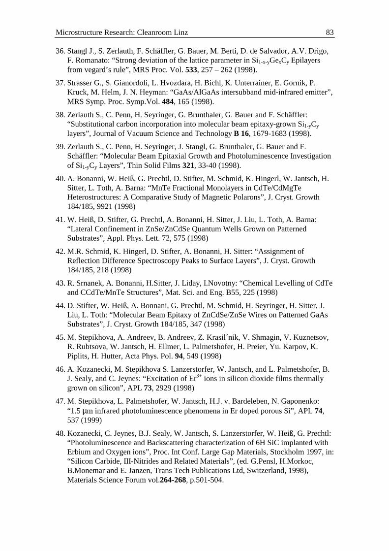
Microstructure Research: Cleanroom Linz 83
36. Stangl J., S. Zerlauth, F. Schäffler, G. Bauer, M. Berti, D. de Salvador, A.V. Drigo,F. Romanato: “Strong deviation of the lattice parameter in Si1-x-yGexCy Epilayersfrom vegard’s rule”, MRS Proc. Vol. 533, 257 – 262 (1998).
37. Strasser G., S. Gianordoli, L. Hvozdara, H. Bichl, K. Unterrainer, E. Gornik, P.Kruck, M. Helm, J. N. Heyman: “GaAs/AlGaAs intersubband mid-infrared emitter”,MRS Symp. Proc. Symp.Vol. 484, 165 (1998).
38. Zerlauth S., C. Penn, H. Seyringer, G. Brunthaler, G. Bauer and F. Schäffler:“Substitutional carbon incorporation into molecular beam epitaxy-grown Si1-yCy
layers”, Journal of Vacuum Science and Technology B 16, 1679-1683 (1998).
39. Zerlauth S., C. Penn, H. Seyringer, J. Stangl, G. Brunthaler, G. Bauer and F.Schäffler: “Molecular Beam Epitaxial Growth and Photoluminescence Investigationof Si1-yCy Layers”, Thin Solid Films 321, 33-40 (1998).
40. A. Bonanni, W. Heiß, G. Prechtl, D. Stifter, M. Schmid, K. Hingerl, W. Jantsch, H.Sitter, L. Toth, A. Barna: “MnTe Fractional Monolayers in CdTe/CdMgTeHeterostructures: A Comparative Study of Magnetic Polarons”, J. Cryst. Growth184/185, 9921 (1998)
41. W. Heiß, D. Stifter, G. Prechtl, A. Bonanni, H. Sitter, J. Liu, L. Toth, A. Barna:“Lateral Confinement in ZnSe/ZnCdSe Quantum Wells Grown on PatternedSubstrates”, Appl. Phys. Lett. 72, 575 (1998)
42. M.R. Schmid, K. Hingerl, D. Stifter, A. Bonanni, H. Sitter: “Assignment ofReflection Difference Spectroscopy Peaks to Surface Layers”, J. Cryst. Growth184/185, 218 (1998)
43. R. Srnanek, A. Bonanni, H.Sitter, J. Liday, I.Novotny: “Chemical Levelling of CdTeand CCdTe/MnTe Structures”, Mat. Sci. and Eng. B55, 225 (1998)
44. D. Stifter, W. Heiß, A. Bonnani, G. Prechtl, M. Schmid, H. Seyringer, H. Sitter, J.Liu, L. Toth: “Molecular Beam Epitaxy of ZnCdSe/ZnSe Wires on Patterned GaAsSubstrates”, J. Cryst. Growth 184/185, 347 (1998)
45. M. Stepikhova, A. Andreev, B. Andreev, Z. Krasil´nik, V. Shmagin, V. Kuznetsov,R. Rubtsova, W. Jantsch, H. Ellmer, L. Palmetshofer, H. Preier, Yu. Karpov, K.Piplits, H. Hutter, Acta Phys. Pol. 94, 549 (1998)
46. A. Kozanecki, M. Stepikhova S. Lanzerstorfer, W. Jantsch, and L. Palmetshofer, B.J. Sealy, and C. Jeynes: “Excitation of Er3+ ions in silicon dioxide films thermallygrown on silicon”, APL 73, 2929 (1998)
47. M. Stepikhova, L. Palmetshofer, W. Jantsch, H.J. v. Bardeleben, N. Gaponenko:“1.5 µm infrared photoluminescence phenomena in Er doped porous Si”, APL 74,537 (1999)
48. Kozanecki, C. Jeynes, B.J. Sealy, W. Jantsch, S. Lanzerstorfer, W. Heiß, G. Prechtl:“Photoluminescence and Backscattering characterization of 6H SiC implanted withErbium and Oxygen ions”, Proc. Int Conf. Large Gap Materials, Stockholm 1997, in:“Silicon Carbide, III-Nitrides and Related Materials”, (ed. G.Pensl, H.Morkoc,B.Monemar and E. Janzen, Trans Tech Publications Ltd, Switzerland, 1998),Materials Science Forum vol.264-268, p.501-504.
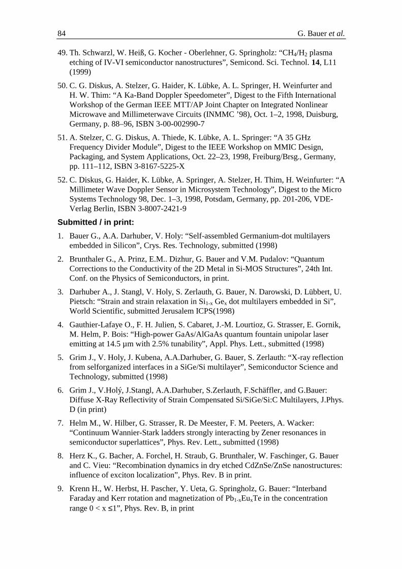
84 G. Bauer et al.
49. Th. Schwarzl, W. Heiß, G. Kocher - Oberlehner, G. Springholz: “CH4/H2 plasmaetching of IV-VI semiconductor nanostructures”, Semicond. Sci. Technol. 14, L11(1999)
50. C. G. Diskus, A. Stelzer, G. Haider, K. Lübke, A. L. Springer, H. Weinfurter andH. W. Thim: “A Ka-Band Doppler Speedometer”, Digest to the Fifth InternationalWorkshop of the German IEEE MTT/AP Joint Chapter on Integrated NonlinearMicrowave and Millimeterwave Circuits (INMMC ’98), Oct. 1–2, 1998, Duisburg,Germany, p. 88–96, ISBN 3-00-002990-7
51. A. Stelzer, C. G. Diskus, A. Thiede, K. Lübke, A. L. Springer: “A 35 GHzFrequency Divider Module”, Digest to the IEEE Workshop on MMIC Design,Packaging, and System Applications, Oct. 22–23, 1998, Freiburg/Brsg., Germany,pp. 111–112, ISBN 3-8167-5225-X
52. C. Diskus, G. Haider, K. Lübke, A. Springer, A. Stelzer, H. Thim, H. Weinfurter: “AMillimeter Wave Doppler Sensor in Microsystem Technology”, Digest to the MicroSystems Technology 98, Dec. 1–3, 1998, Potsdam, Germany, pp. 201-206, VDE-Verlag Berlin, ISBN 3-8007-2421-9
Submitted / in print:
1. Bauer G., A.A. Darhuber, V. Holy: “Self-assembled Germanium-dot multilayersembedded in Silicon”, Crys. Res. Technology, submitted (1998)
2. Brunthaler G., A. Prinz, E.M.. Dizhur, G. Bauer and V.M. Pudalov: “QuantumCorrections to the Conductivity of the 2D Metal in Si-MOS Structures”, 24th Int.Conf. on the Physics of Semiconductors, in print.
3. Darhuber A., J. Stangl, V. Holy, S. Zerlauth, G. Bauer, N. Darowski, D. Lübbert, U.Pietsch: “Strain and strain relaxation in Si1-x Gex dot multilayers embedded in Si”,World Scientific, submitted Jerusalem ICPS(1998)
4. Gauthier-Lafaye O., F. H. Julien, S. Cabaret, J.-M. Lourtioz, G. Strasser, E. Gornik,M. Helm, P. Bois: “High-power GaAs/AlGaAs quantum fountain unipolar laseremitting at 14.5 µm with 2.5% tunability”, Appl. Phys. Lett., submitted (1998)
5. Grim J., V. Holy, J. Kubena, A.A.Darhuber, G. Bauer, S. Zerlauth: “X-ray reflectionfrom selforganized interfaces in a SiGe/Si multilayer”, Semiconductor Science andTechnology, submitted (1998)
6. Grim J., V.Holý, J.Stangl, A.A.Darhuber, S.Zerlauth, F.Schäffler, and G.Bauer:Diffuse X-Ray Reflectivity of Strain Compensated Si/SiGe/Si:C Multilayers, J.Phys.D (in print)
7. Helm M., W. Hilber, G. Strasser, R. De Meester, F. M. Peeters, A. Wacker:“Continuum Wannier-Stark ladders strongly interacting by Zener resonances insemiconductor superlattices”, Phys. Rev. Lett., submitted (1998)
8. Herz K., G. Bacher, A. Forchel, H. Straub, G. Brunthaler, W. Faschinger, G. Bauerand C. Vieu: “Recombination dynamics in dry etched CdZnSe/ZnSe nanostructures:influence of exciton localization”, Phys. Rev. B in print.
9. Krenn H., W. Herbst, H. Pascher, Y. Ueta, G. Springholz, G. Bauer: “InterbandFaraday and Kerr rotation and magnetization of Pb1-xEuxTe in the concentrationrange 0 < x ≤1”, Phys. Rev. B, in print
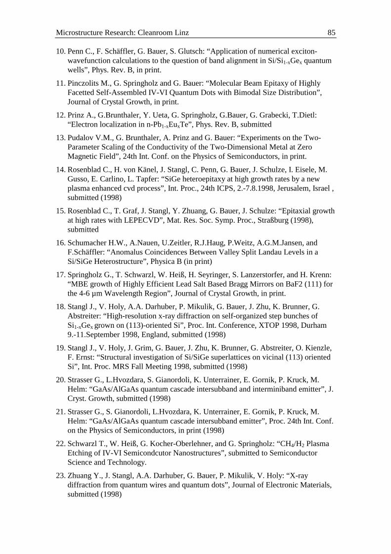
Microstructure Research: Cleanroom Linz 85
10. Penn C., F. Schäffler, G. Bauer, S. Glutsch: “Application of numerical exciton-wavefunction calculations to the question of band alignment in Si/Si1-xGex quantumwells”, Phys. Rev. B, in print.
11. Pinczolits M., G. Springholz and G. Bauer: “Molecular Beam Epitaxy of HighlyFacetted Self-Assembled IV-VI Quantum Dots with Bimodal Size Distribution”,Journal of Crystal Growth, in print.
12. Prinz A., G.Brunthaler, Y. Ueta, G. Springholz, G.Bauer, G. Grabecki, T.Dietl:“Electron localization in n-Pb1-xEuxTe”, Phys. Rev. B, submitted
13. Pudalov V.M., G. Brunthaler, A. Prinz and G. Bauer: “Experiments on the Two-Parameter Scaling of the Conductivity of the Two-Dimensional Metal at ZeroMagnetic Field”, 24th Int. Conf. on the Physics of Semiconductors, in print.
14. Rosenblad C., H. von Känel, J. Stangl, C. Penn, G. Bauer, J. Schulze, I. Eisele, M.Gusso, E. Carlino, L. Tapfer: “SiGe heteroepitaxy at high growth rates by a newplasma enhanced cvd process”, Int. Proc., 24th ICPS, 2.-7.8.1998, Jerusalem, Israel ,submitted (1998)
15. Rosenblad C., T. Graf, J. Stangl, Y. Zhuang, G. Bauer, J. Schulze: “Epitaxial growthat high rates with LEPECVD”, Mat. Res. Soc. Symp. Proc., Straßburg (1998),submitted
16. Schumacher H.W., A.Nauen, U.Zeitler, R.J.Haug, P.Weitz, A.G.M.Jansen, andF.Schäffler: “Anomalus Coincidences Between Valley Split Landau Levels in aSi/SiGe Heterostructure”, Physica B (in print)
17. Springholz G., T. Schwarzl, W. Heiß, H. Seyringer, S. Lanzerstorfer, and H. Krenn:“MBE growth of Highly Efficient Lead Salt Based Bragg Mirrors on BaF2 (111) forthe 4-6 µm Wavelength Region”, Journal of Crystal Growth, in print.
18. Stangl J., V. Holy, A.A. Darhuber, P. Mikulik, G. Bauer, J. Zhu, K. Brunner, G.Abstreiter: “High-resolution x-ray diffraction on self-organized step bunches ofSi1-xGex grown on (113)-oriented Si”, Proc. Int. Conference, XTOP 1998, Durham9.-11.September 1998, England, submitted (1998)
19. Stangl J., V. Holy, J. Grim, G. Bauer, J. Zhu, K. Brunner, G. Abstreiter, O. Kienzle,F. Ernst: “Structural investigation of Si/SiGe superlattices on vicinal (113) orientedSi”, Int. Proc. MRS Fall Meeting 1998, submitted (1998)
20. Strasser G., L.Hvozdara, S. Gianordoli, K. Unterrainer, E. Gornik, P. Kruck, M.Helm: “GaAs/AlGaAs quantum cascade intersubband and interminiband emitter”, J.Cryst. Growth, submitted (1998)
21. Strasser G., S. Gianordoli, L.Hvozdara, K. Unterrainer, E. Gornik, P. Kruck, M.Helm: “GaAs/AlGaAs quantum cascade intersubband emitter”, Proc. 24th Int. Conf.on the Physics of Semiconductors, in print (1998)
22. Schwarzl T., W. Heiß, G. Kocher-Oberlehner, and G. Springholz: “CH4/H2 PlasmaEtching of IV-VI Semicondcutor Nanostructures”, submitted to SemiconductorScience and Technology.
23. Zhuang Y., J. Stangl, A.A. Darhuber, G. Bauer, P. Mikulik, V. Holy: “X-raydiffraction from quantum wires and quantum dots”, Journal of Electronic Materials,submitted (1998)
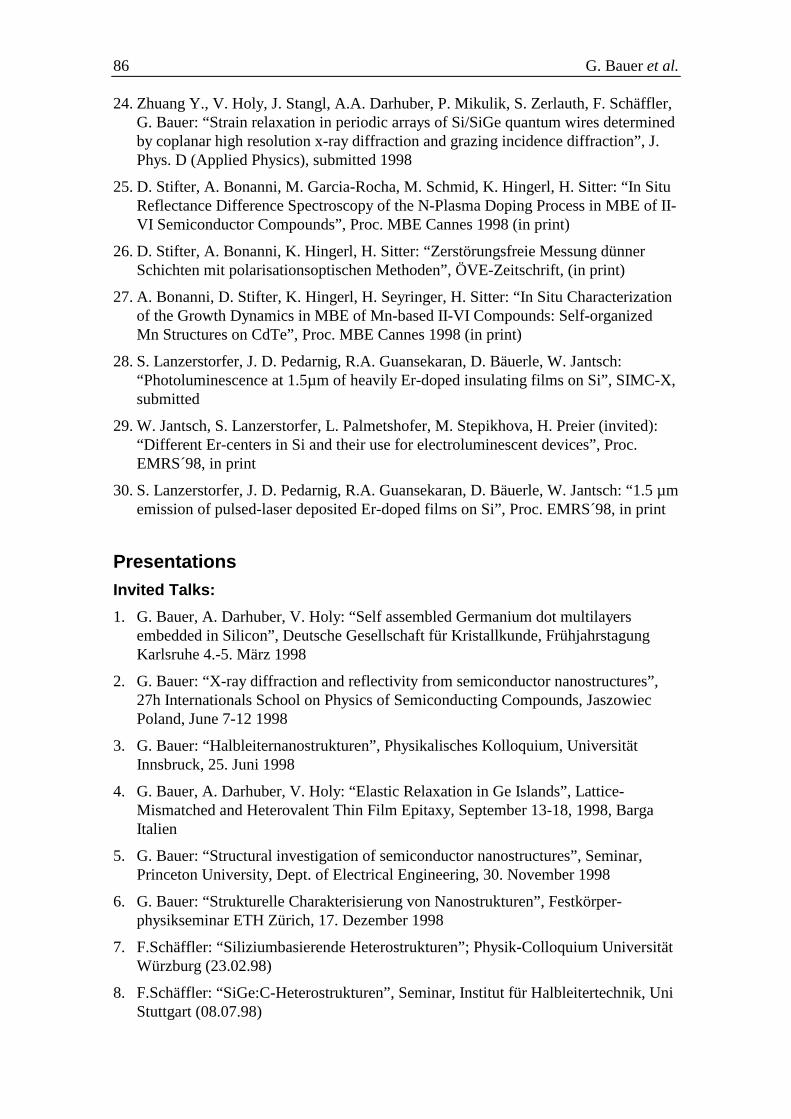
86 G. Bauer et al.
24. Zhuang Y., V. Holy, J. Stangl, A.A. Darhuber, P. Mikulik, S. Zerlauth, F. Schäffler,G. Bauer: “Strain relaxation in periodic arrays of Si/SiGe quantum wires determinedby coplanar high resolution x-ray diffraction and grazing incidence diffraction”, J.Phys. D (Applied Physics), submitted 1998
25. D. Stifter, A. Bonanni, M. Garcia-Rocha, M. Schmid, K. Hingerl, H. Sitter: “In SituReflectance Difference Spectroscopy of the N-Plasma Doping Process in MBE of II-VI Semiconductor Compounds”, Proc. MBE Cannes 1998 (in print)
26. D. Stifter, A. Bonanni, K. Hingerl, H. Sitter: “Zerstörungsfreie Messung dünnerSchichten mit polarisationsoptischen Methoden”, ÖVE-Zeitschrift, (in print)
27. A. Bonanni, D. Stifter, K. Hingerl, H. Seyringer, H. Sitter: “In Situ Characterizationof the Growth Dynamics in MBE of Mn-based II-VI Compounds: Self-organizedMn Structures on CdTe”, Proc. MBE Cannes 1998 (in print)
28. S. Lanzerstorfer, J. D. Pedarnig, R.A. Guansekaran, D. Bäuerle, W. Jantsch:“Photoluminescence at 1.5µm of heavily Er-doped insulating films on Si”, SIMC-X,submitted
29. W. Jantsch, S. Lanzerstorfer, L. Palmetshofer, M. Stepikhova, H. Preier (invited):“Different Er-centers in Si and their use for electroluminescent devices”, Proc.EMRS´98, in print
30. S. Lanzerstorfer, J. D. Pedarnig, R.A. Guansekaran, D. Bäuerle, W. Jantsch: “1.5 µmemission of pulsed-laser deposited Er-doped films on Si”, Proc. EMRS´98, in print
PresentationsInvited Talks:
1. G. Bauer, A. Darhuber, V. Holy: “Self assembled Germanium dot multilayersembedded in Silicon”, Deutsche Gesellschaft für Kristallkunde, FrühjahrstagungKarlsruhe 4.-5. März 1998
2. G. Bauer: “X-ray diffraction and reflectivity from semiconductor nanostructures”,27h Internationals School on Physics of Semiconducting Compounds, JaszowiecPoland, June 7-12 1998
3. G. Bauer: “Halbleiternanostrukturen”, Physikalisches Kolloquium, UniversitätInnsbruck, 25. Juni 1998
4. G. Bauer, A. Darhuber, V. Holy: “Elastic Relaxation in Ge Islands”, Lattice-Mismatched and Heterovalent Thin Film Epitaxy, September 13-18, 1998, BargaItalien
5. G. Bauer: “Structural investigation of semiconductor nanostructures”, Seminar,Princeton University, Dept. of Electrical Engineering, 30. November 1998
6. G. Bauer: “Strukturelle Charakterisierung von Nanostrukturen”, Festkörper-physikseminar ETH Zürich, 17. Dezember 1998
7. F.Schäffler: “Siliziumbasierende Heterostrukturen”; Physik-Colloquium UniversitätWürzburg (23.02.98)
8. F.Schäffler: “SiGe:C-Heterostrukturen”, Seminar, Institut für Halbleitertechnik, UniStuttgart (08.07.98)
Microstructure Research: Cleanroom Linz 87
9. F.Schäffler: “Siliziumbasierende Heterostrukturen”, Seminar, Institut fürFestkörperelektronik, TU Wien (19.06.98)
10. V. M. Pudalov: “Metal-Insulator Transition in Two Dimensions”, 10th InternationalWinterschool on New Developements in Solid State Physics, NEW FRONTIERS INLOW-DIMENSIONAL PHYSICS, 23-27 February, 1998, Mauterndorf, Province ofSalzburg, Austria
11. M. Helm: “Energierelaxation von Elektronen in Halbleiter-Quantenstrukturen:infrarot-spektroskopische Untersuchungen”, Forschungszentrum Rossendorf,Deutschland, 4.6.1998.
12. M. Helm: “Minibands and Wannier-Stark-ladders in semiconductor superlatticesstudied by infrared spectroscopy”, Imperial College, London, UK, 19.11.1998.
13. G. Springholz: “Fabrication of Semiconductor Quantum Dots: FromNanolithography to Self-Organisation”, Austrian Physical Society Annual Meeting,13. - 18.9. 1998, Graz, Austria.
14. G. Springholz: “Self-Organisation of Semiconductor Quantum Dots: Synthesis ofthree-dimensional Quantum dot crystals”, Physik Kolloquium der UniversitätRegensburg, 16.11.1998, Regensburg, BRD.
15. W. Jantsch, S. Lanzerstorfer, L. Palmetshofer, M. Stepikhova, H. Preier: “DifferentEr-centers in Si and their use for electroluminescent devices”, European MaterialsResearch Society Meeting, Strassburg 1998
Conference presentations (talks and posters):
1. C.Schelling, F.Schäffler: “Step-Bunching von SiGe auf verkippten Si(001)Substraten”, MBE-Tagung, Hamburg 22.09.98
2. C.Schelling, J.Stangl, G.Bauer, F.Schäffler: “Step-Bunching in Si1-xGex Layers withMismatch <1%”, MRS Fall-Meeting, Boston 03.12.98
3. G. Brunthaler, A. Prinz, E.M. Dizhur, G. Bauer, V.M. Pudalov: “Quantumcorrections to the conductivity of the 2D metal in Si-Mos structures”, 24thInternational Conference on the Physics of Semiconductors, Jerusalem Israel, 2.-7.August 1998.
4. V.M. Pudalov, G. Brunthaler, A. Prinz, G. Bauer: “Experiments on the two-parameter scaling of the conductivity of the two-dimensional metal at zero magneticfield, 24th International Conference on the Physics of Semiconductors, JerusalemIsrael, 2.-7. August 1998.
5. J. Stangl, G.Bauer, S. Zerlauth, F. Schäffler, M. Berti, D. De Salvador, A.V. Drigo.F. Romanato: “Deviation from Lattice Parameter from Vegard’s Rule in Si1-x-yGexCy
Epilayers”, 24th International Conference on the Physics of Semiconductors,Jerusalem Israel, 2.-7. August 1998.
6. A.A. Darhuber, V. Holy, J. Stangl, S. Zerlauth, G. Bauer: “Strain and strainrelaxation in SiGe dot multilayers embedded in Si”, 24th International Conferenceon the Physics of Semiconductors, Jerusalem Israel, 2.-7. August 1998.
7. C. Rosenblad, T. Graf. J. Stangl, C. Penn, G. Bauer, H.v.Känel: “Si-Ge hetero-epitaxy at high growth rates by a new plasma enhanced CVD process”, 24th
88 G. Bauer et al.
International Conference on the Physics of Semiconductors, Jerusalem Israel, 2.-7.August 1998.
8. J. Stangl, V. Holy, G. Bauer , J.Zhu, K. Brunner, G.Abstreiter: “StructuralInvestigation of Si/SiGe Superlattices on vicinal (113) oriented Si”, MRS FallMeeting, Boston U.S.A., Dezember 1998
9. C. Schelling, J. Stangl, G. Bauer, F. Schäffler: “Step Bunching in Si1-xGex layerswith mismatch ≥ 1 %”, MRS Fall Meeting, 30.11- 4.12.1998, Boston U.S.A.
10. Julian Stangl: “Lattice Parameter in Si1-yCy and Si1-x-yGexCy Epilayers: StrongDeviations from Vegard’s Rule”, MRS Spring Meeting, San Francisco, 13-17. April1998
11. C. Penn, P.C.M. Christianen, F. Schäffler, J.C. Maan, G. Bauer: “Photolumin-escence from Si/Si1-xGex Single Quantum Wells in High Magnetic Fields: Localizedand Free excition Recombination”, 13th International Conference on High MagneticFields in Semiconductor Physics, SemiMag 13, Nijmegen, 10.-14. August 1998
12. A. Prinz, Y. Ueta, G. Springholz, G. Brunthaler, G. Bauer, G. Grabecki, M. Sawickiand T. Dietl: “Electron localization in n-Pb1-xEuxTe”, (Poster), WinterschuleMauterndorf, Feb. 1998.
13. G. Strasser, L.Hvozdara, S. Gianordoli, K. Unterrainer, E. Gornik, P. Kruck, M.Helm: “GaAs/AlGaAs quantum cascade intersubband and interminiband emitter”,10th Int. Conf. on Molecular Beam Epitaxy, 31.8. – 4.9.98 Cannes, France
14. G. Strasser, S. Gianordoli, L.Hvozdara, K. Unterrainer, E. Gornik, P. Kruck, M.Helm: “GaAs/AlGaAs quantum cascade intersubband emitter”, 24th Int. Conf. onthe Physics of Semiconductors (ICPS 24), Jerusalem, Israel, Aug. 1998
15. P. Kruck, M. Helm, G. Strasser, L. Hvozdara, S. Gianordoli, K. Unterrainer, E.Gornik: “Quantenkaskaden-Emitter auf GaAs-Basis”, 28. IR-Kolloquium desFraunhofer-Instituts für Angwandte Festkörperphysik, Freiburg, Gemany, April1998
16. P. Kruck, M. Helm, G. Bauer, J. F. Nützel, G. Abstreiter: “p-type Si/SiGe normal-incidence quantum well infrared detectors”, 28. IR-Kolloquium des Fraunhofer-Instituts für Angewandte Festkörperphysik, Freiburg, Gemany, April 1998
17. G. Springholz, T. Schwarzl, W. Heiß and H. Krenn: “MBE growth of highlyefficient lead-salt based Bragg mirrors on BaF2 (111) for the 4 - 6 µm wavelenghtregion”, 10th International Conference on Molecular Beam Epitaxy, 31.8. -4.9.1998, Cannes, France.
18. G. Springholz, M. Pinczolits, V. Holy and G. Bauer: “Nearly perfect threedimensional ordering of self-assembled PbSe quantum dots in strain symmetrizedPbSe/PbEuTe superlattices grown by molecular beam epitaxy”, Fall Meeting of theMaterials Research Society, 30.11. - 4.12.1998, Boston USA.
19. G. Springholz, T. Schwarzl, W. Heiss: “Fabrication of lead salt-based Bragg mirrorsand microcavities for 4 to 7 µm mid-infrared diode lasers”, Fall Meeting of theMaterials Research Society, 30.11. - 4.12.1998, Boston USA.
20. M. Pinczolits, G. Springholz, and G. Bauer: “Molecular Beam Epitaxy of highlyfacetted self-assembled IV-VI quantum dots with bimodal size distribution”, 10th
Microstructure Research: Cleanroom Linz 89
International Conference on Molecular Beam Epitaxy, 31.8. - 4.9.1998, Cannes,France.
21. M. Pinczolits, G. Springholz and G. Bauer: “Direct Growth of PbSe Quantum Dotson PbTe (111)”, Spring Meeting of the German Physical Society, 23.-27.3.1998,Regensburg, Germany.
22. G. Springholz and F. Köck: “Scanning tunneling microscopy of misfit dislocationsin multilayer heterostructures: depth resolution and dislocation reactions”, 10thInternational Conference on Molecular Beam Epitaxy, 31.8. - 4.9.1998, Cannes,France.
23. K. Wiesauer and G. Springholz: “Nanolithography of Semiconducturs bynanoidentation of Photoresists”, 48th Annual Meeting of the Austrian PhysicalSociety, 15.9.- 18.9.1998, Graz, Austria.
24. C. Pidgeon, P. Findlay, B. N. Mrudin, C. J. G. M. Langerak, C. Ciesla, J. Oswald, A.Homer, G. Springholz, and G. Bauer: “Auger recombination dynamics of lead saltsunder ps free electron laser excitation”, (poster), 24th International Conference onthe Physics of Semiconductors, 2. 7. 8.1998, Jerusalem, Israel.
25. J. H. Li, G. Springholz, H. Seyringer, V. Holy, F. Schäffler and G. Bauer: “Strainrelaxation and surface morphology of compositionally graded Si/Si1-xGex buffers”,International Workshop on Silicon-Germannium Heterostructures, 16.9.-20.9.1997,Barga, Italy.
26. D. Stifter, A. Bonanni, M. Garcia-Rocha, M. Schmid, K. Hingerl, H. Sitter: “In-situreflectance difference spectroscopy: N-plasma doping process of MBE-grown ZnTelayers”, 10th Int. Conference on MBE, Cannes, France 1998
27. A. Bonanni, D. Stifter, K. Hingerl, H. Seyringer, H. Sitter: “In-situ characterizationof the growth dynamics in MBE of Mn-based II-VI compounds: self-organized Mnstructures on CdTe”, 10th Int. Conference on MBE, Cannes, France 1998
28. A. Bonanni, D. Stifter, K. Hingerl, H. Seyringer, H. Sitter: “Self-organized magneticand semimagnetic islands on CdTe”, Jahrestagung der ÖPG, Wien 1998
29. D. Stifter, A. Bonanni, M. Garcia-Rocha, M. Schmid, K. Hingerl, H. Sitter: “In-situreflectance difference spectroscopy: N-plasma doping process of MBE-grown ZnTelayers”, Jahrestagung der ÖPG, Wien 1998
30. I.A. Karpovich, M.V. Stepikhova, W. Jantsch: “Heteroepitaxial passivation of GaAssurfaces and its influence on the photosensitivity spectra and recombinationparameters of GaAs epitaxial layers and semi-insulating materials”, Int. Conf.Semiconductors and Insulators, Berkeley 1998
31. S. Lanzerstorfer, W. Jantsch, M. Stepikhova, L. Palmetshofer, H. Preier: “Whichtype of center is responsible for the 1.54 µm emission in Si:Er at 300K?”, Int.Conference on the Physics of Semiconductors, Jerusalem 1998
32. A. Kozanecki, W. Jantsch, M. Stepikhova, S. Lanzerstorfer, A. Henry, J.P.Bergmann: “Spectroscopic characterization of Er3+ ions in 6H SiC”, Int. Conferenceon the Physics of Semiconductors, Jerusalem 1998
33. W. Jantsch, W. Wilamowski, N. Sandersfeld, F. Schäffler: “ESR investigations ofmodulation doped Si/SiGe quantum wells”, Int. Conference on Shallow Levels inSemiconductors, Montpellier 1998
90 G. Bauer et al.
34. S. Lanzerstorfer, J. D. Pedarnig, R.A. Guansekaran, D. Bäuerle, W. Jantsch:“Photoluminescence at 1.5 µm of heavily Er-doped insulating films on Si”, Int.Conf. Semiconductors and Insulators, Berkeley 1998
35. S. Lanzerstorfer, J. D. Pedarnig, R.A. Guansekaran, D. Bäuerle, W. Jantsch: “1.5 µmemission of pulsed-laser deposited Er-doped films on Si”, European MaterialsResearch Society Meeting, Strassburg 1998
36. W. Jantsch, F. Schäffler, Z. Wilamowski: “Characterization of SiGe Quantum Wellsby Conduction Electron Spin Resonance Spectroscopy”, Herbsttreffen desVerbundes “Nanoelektronik”, Walter-Schottky Institut der TU München, 8. Oktober1998.
37. C. G. Diskus, A. Stelzer, K. Lübke, A. L. Springer, G. Haider, H. W. Thim: “AMatched InGaAs Detector Diode for a Ka-Band Radar Front-End”, Digest to the22nd Workshop on Compound Semiconductor Devices and Integrated Circuits(WOCSDICE ’98), May 24–27, 1998, Zeuthen/Berlin, Germany, pp. 135–136
38. C. G. Diskus, A. Stelzer, K. Lübke, A. L. Springer, H. W. Thim: “A Ka-BandDoppler-Sensor”, Proceedings of the 6th UK Mechatronics Forum InternationalConference (Mechatronics ‘98), Sept. 9–11, 1998, Skövde/Sweden, 1998 Pergamon,Elsevier Science Ltd. Oxford, pp. 565–570. ISBN 0-08-043339-1
Doctor’s Theses1. Dipl.-Ing. Anton Darhuber, “Strukturelle Untersuchungen von Halbleiternano-
strukturen mittels hochauflösender Röntgenbeugung und -Reflexion”, Linz, 1998.
2. M.Sc. Dana Papajova, “Simulation of epitaxial growth by a rate equation model”,Linz, 1998.
3. Dipl.-Ing. David Stifter, “MBE of II-VI semiconductor heterostructures:Growth,doping and characterization”, Linz, 1998.
4. M.Sc. Manh Tuan Nguyen, “Growth, doping and characterization of C60 epilayersgrown by hot wall epitaxy”, Linz, 1998.
Habilitations1. G. Brunthaler, “Lokalisierung von Ladungsträgern in Halbleitersystemen”, Linz
1998.
Cooperations1. Siemens München, Dr.Heide
2. Daimler Benz Reserach Laboratories Ulm, Dr. Presting, Dr. König
3. VOEST ALPINE, Linz, Dr.Angerer,
4. Siemens Villach,
5. AMS Unterpremstätten, Dr.Fromherz
6. KEBA, Linz, Ing.G.Krippner
Microstructure Research: Cleanroom Linz 91
7. Institut für Halbleiterphysik, Frankfurt/Oder
8. Sektion Physik, Ludwig-Maximilians Universität München
9. Physics Department, Cornell University
10. ETH, Zürich
11. ESRF Grenoble
12. DESY, Hasylab, Hamburg
13. FOM Institute Rijnhuizen, Niederlande
14. Walter Schottky Institut, TU München
15. IBM Research Center, Yorktown Heights
16. Institut für Festkörperelektronik, TU Wien
17. Philips Almelo, Niederlande
18. Heriot Watt University, Edinburgh, Scotland
19. University of Southampton, England
20. High Pressure Research Center, Warschau, Polen
21. Institue of Physics, Polish Academy of Sciences, Warschau
22. TU Berlin, Institut für Festkörperphysik
23. Universität Würzburg
24. Universität Bayreuth
25. Universität Bremen
26. Purdue University, Lafayette, IN, USA
27. MIT, Cambridge, MA, USA
28. NIST, Gaithersburg, MD, USA
29. Nanoelectronics Research Center, University of Glasgow, Scotland
30. University of Warwick, Coventry, England
31. North Carolina State University, NC, USA
32. IAF Freiburg
33. CENG Grenoble
34. Universität Paderborn
35. INSA, Lyon
36. Université de Montpellier
37. ELETTRA, Triest
38. Universiteit Instelling, Antwerpen, Niederlande
39. TASC Triest
40. ENEA, Roma
41. CNRSM-PASTIS, Brindisi

92 G. Bauer et al.
42. Akademie der Wissenschaften, Troits, Moskau
43. High Magnetic Field Lab., Grenoble
44. Siemens München, Zentrale Technik, Bereich Halbleiter
45. Fraunhofer-Institut (IAF) Freiburg (Chiptechnologie)
46. TU-München (Mikrowellentechnik)
The Society for Microelectronics – Annual Report 1999 93
A Ka-Band Detector Diode with HighSensitivity
C. G. Diskus, A. Stelzer, K. Lübke, H. W. Thim
Microelectronics Institute, Johannes Kepler UniversityAltenberger Str. 69, 4040 Linz, Austria
In this work the design and matching of a zero bias InGaAs-Schottky detector diodefor 35 GHz is described. High voltage sensitivity at zero bias is achieved by incorpo-rating indium and by matching the input impedance to 50 Ω. This diode is used asthe receiving part of a Doppler-radar front-end.
1. IntroductionIn millimeter-wave systems suited for automotive applications Schottky-barrier diodesare used for detecting and mixing signals because of their high switching speed whichresults from the unipolar conduction mechanism. III-V semiconductors are the preferredmaterials because of their higher electron mobility at low fields compared to Silicon.Important parameters of Schottky barrier detector diodes are series resistance, barrierheight, and junction capacitance. There are two types of detector diodes: zero-bias de-vices and detector diodes used with bias, which need a more complicated circuitry.
2. InGaAs DiodeThe voltage sensitivity of a detector diode is a function of its reverse saturation current[1]. For optimum sensitivity this current has to be in the range of 10–6 A. To achieve thisvalue with GaAs technology at zero bias – which is desirable to keep the circuit as sim-ple as possible – the barrier height must be tailored to 0.22 – 0.25 eV by incorporatingindium. With increasing In content the energy gap of the semiconductor is lowered from1.42 eV (GaAs) to 0.33 eV (InAs). With In0.38Ga0.62As the desired barrier height of theSchottky contact can be achieved.
The diodes were fabricated using epitaxial layers of GaAs and InGaAs grown by metalorganic chemical vapor deposition (MOCVD) on GaAs-substrates. Ni/GeAu/Ni/Aufilms were evaporated thermally and by e-beam, respectively, and annealed to form oh-mic contacts on n-type layers, Ti/Au and Cr/Au were evaporated and used for Schottkycontacts. The ohmic contacts were recessed by wet chemical etching and the connectionto the Schottky contact on the top was led over a SiO2 bridge. The SiO2 layers wereetched in a reactive ion etching (RIE) reactor. The patterns for the contact pads, the in-terconnections and the circuit were transferred to the substrate using e-beam lithogra-phy. The layer sequence of the Schottky-barrier diodes is shown in Fig. 1. Details of thefabrication can be found in [2].
94 C. G. Diskus et al.
n+ -InGaAs 2,7⋅1018
InxGa1-xAs (0<x<0.38)
Buffer Layer
Semi-InsulatingGaAs-Substrate
Schottky
n –InGaAs4⋅1016
0,8 µm
0,8 µm
0,18 µmohmic
Anode Cathode
450 µm
Fig. 1: Layer sequence.
The DC parameters were determined from computer controlled I-V measurements. Themeasured forward current-voltage relationship of a typical device is shown on a semi-logarithmic scale in Fig. 2. The semi-logarithmic plot also allows to calculate idealityfactor, series resistance, and barrier height of the devices. A straight line was fitted tothe semi-logarithmic data to extract the parameters. Typical values for reverse saturationcurrent IS, series resistance RS and ideality factor n of diodes with contact area 3x3 µm2
are shown in Table 1.
idealityfactor
saturationcurrent
seriesresistance
barrierheight
capacitance
1.45 8.2⋅10–6 A 9.7 Ω 0.22 V 10.7 fF
Tab. 1: Typical values of In0.38Ga0.62As Schottky barrier diodes (3 µm x 3 µm)
0.00 0.05 0.10 0.15 0.20 0.25
10–3
10–4
10–5
10–6
10–7
10–8
10–9
Cur
rent
(A)
Voltage (V)
Fig. 2: Semi-logarithmic plot of measured current voltage relation.
A Ka-Band Detector Diode with High Sensitivity 95
From the measured junction capacitance of a diode with 100x100 µm2 Schottky contactarea, the junction capacitance for diodes with 3x3 µm2 anode area can be calculated.The resulting cut-off frequency fco = 1/2πRSC for these devices is approximately1500 GHz.
RS = 5,8 Ω
CJ = 90 fFRP = 950 Ω
L = 300 µm
CPW
Fig. 3: Small signal model of the diode.
3. Impedance Matching
A connection of the diode to a 50 Ω microstrip line with no further impedance matchingyielded a sensitivity of 1 mV/µW. In order to enhance sensibility it is necessary to matchthe diode impedance to the 50 Ω of the transmission line.
10 G Hz
67 G Hz
M ode l
M easure m en t
Fig. 4: Reflection coefficient of unmatched diode, frequency range 10 – 67 GHz.
Firstly, a small signal model of the diode was established by fitting the reflection coeffi-cient (S11) of the circuit shown in Fig. 3 to the measured data. The measurement of thediode was accomplished using a vector network analyzer and a wafer prober with copla-
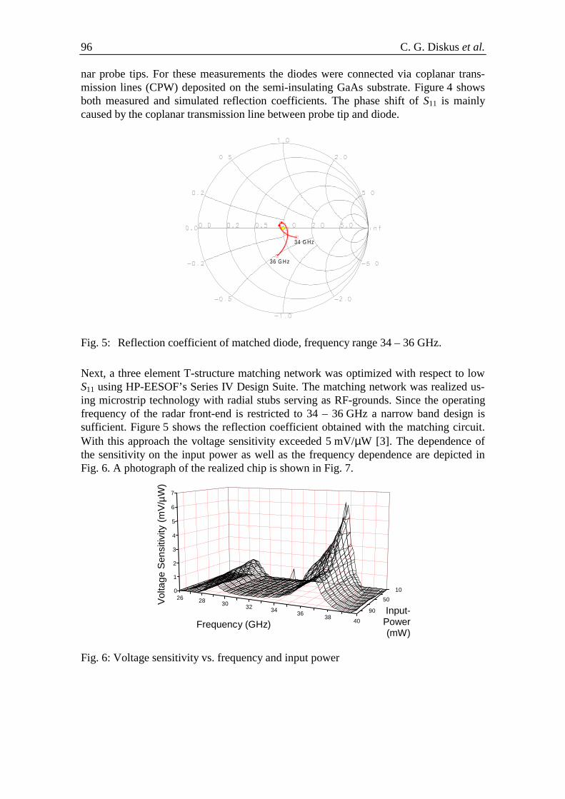
96 C. G. Diskus et al.
nar probe tips. For these measurements the diodes were connected via coplanar trans-mission lines (CPW) deposited on the semi-insulating GaAs substrate. Figure 4 showsboth measured and simulated reflection coefficients. The phase shift of S11 is mainlycaused by the coplanar transmission line between probe tip and diode.
34 G Hz
36 G Hz
Fig. 5: Reflection coefficient of matched diode, frequency range 34 – 36 GHz.
Next, a three element T-structure matching network was optimized with respect to lowS11 using HP-EESOF’s Series IV Design Suite. The matching network was realized us-ing microstrip technology with radial stubs serving as RF-grounds. Since the operatingfrequency of the radar front-end is restricted to 34 – 36 GHz a narrow band design issufficient. Figure 5 shows the reflection coefficient obtained with the matching circuit.With this approach the voltage sensitivity exceeded 5 mV/µW [3]. The dependence ofthe sensitivity on the input power as well as the frequency dependence are depicted inFig. 6. A photograph of the realized chip is shown in Fig. 7.
26 28 30 32 3436
3840
10
50
90
0
1
2
3
4
5
6
7
Frequency (GHz)
Vol
tage
Sen
sitiv
ity (
mV
/ µW
)
Input-Power (mW)
Fig. 6: Voltage sensitivity vs. frequency and input power
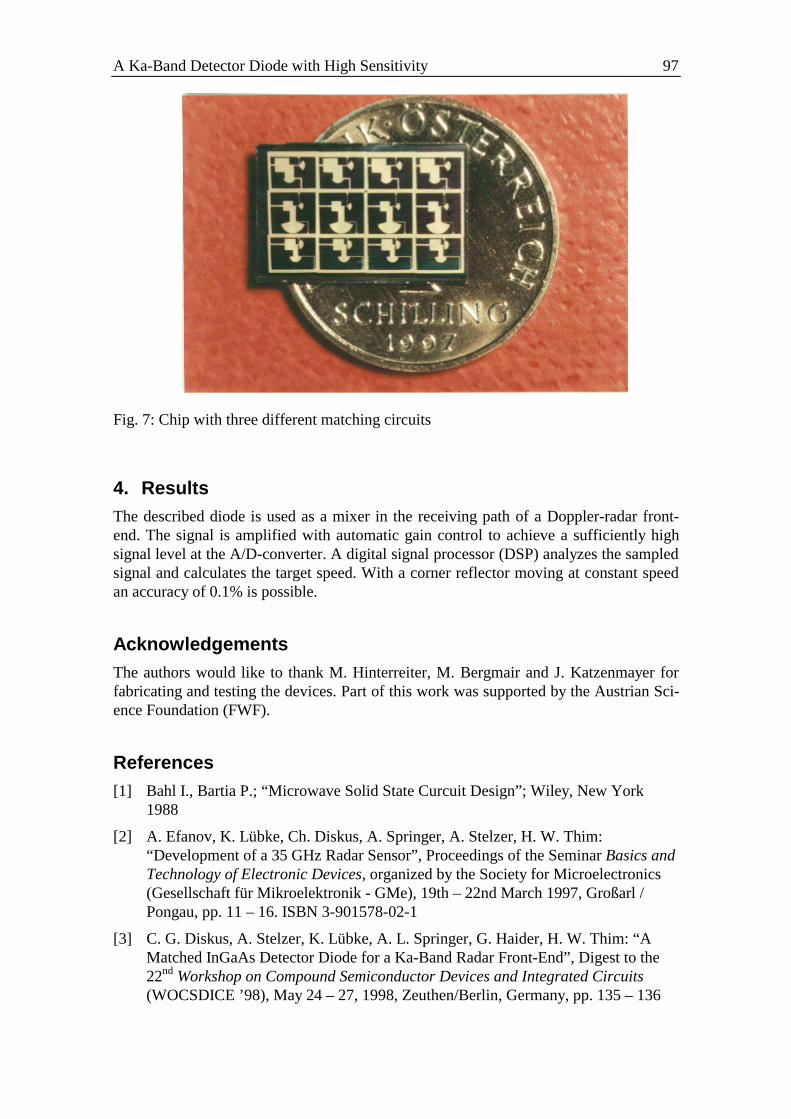
A Ka-Band Detector Diode with High Sensitivity 97
Fig. 7: Chip with three different matching circuits
4. ResultsThe described diode is used as a mixer in the receiving path of a Doppler-radar front-end. The signal is amplified with automatic gain control to achieve a sufficiently highsignal level at the A/D-converter. A digital signal processor (DSP) analyzes the sampledsignal and calculates the target speed. With a corner reflector moving at constant speedan accuracy of 0.1% is possible.
AcknowledgementsThe authors would like to thank M. Hinterreiter, M. Bergmair and J. Katzenmayer forfabricating and testing the devices. Part of this work was supported by the Austrian Sci-ence Foundation (FWF).
References[1] Bahl I., Bartia P.; “Microwave Solid State Curcuit Design”; Wiley, New York
1988
[2] A. Efanov, K. Lübke, Ch. Diskus, A. Springer, A. Stelzer, H. W. Thim:“Development of a 35 GHz Radar Sensor”, Proceedings of the Seminar Basics andTechnology of Electronic Devices, organized by the Society for Microelectronics(Gesellschaft für Mikroelektronik - GMe), 19th – 22nd March 1997, Großarl /Pongau, pp. 11 – 16. ISBN 3-901578-02-1
[3] C. G. Diskus, A. Stelzer, K. Lübke, A. L. Springer, G. Haider, H. W. Thim: “AMatched InGaAs Detector Diode for a Ka-Band Radar Front-End”, Digest to the22nd Workshop on Compound Semiconductor Devices and Integrated Circuits(WOCSDICE ’98), May 24 – 27, 1998, Zeuthen/Berlin, Germany, pp. 135 – 136

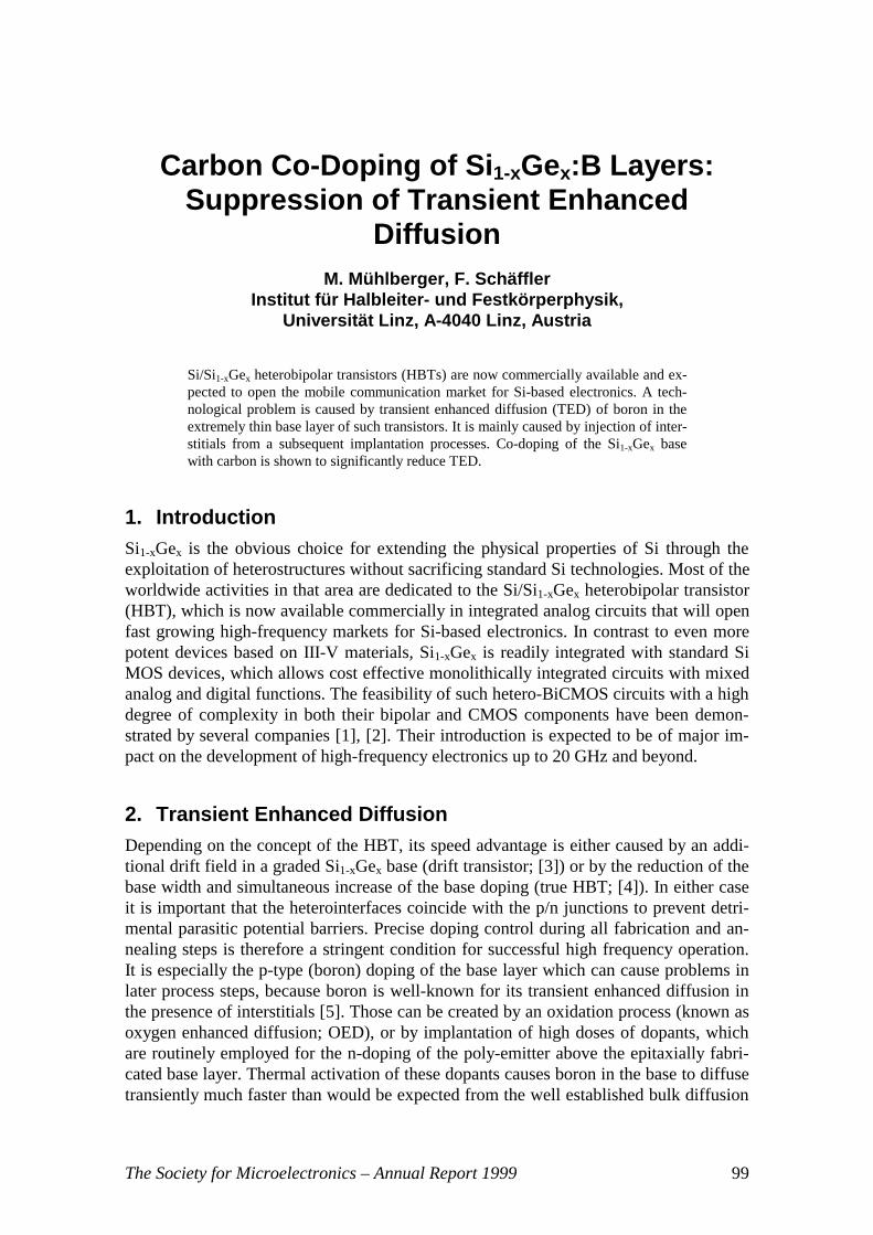
The Society for Microelectronics – Annual Report 1999 99
Carbon Co-Doping of Si 1-xGex:B Layers:Suppression of Transient Enhanced
DiffusionM. Mühlberger, F. Schäffler
Institut für Halbleiter- und Festkörperphysik,Universität Linz, A-4040 Linz, Austria
Si/Si1-xGex heterobipolar transistors (HBTs) are now commercially available and ex-pected to open the mobile communication market for Si-based electronics. A tech-nological problem is caused by transient enhanced diffusion (TED) of boron in theextremely thin base layer of such transistors. It is mainly caused by injection of inter-stitials from a subsequent implantation processes. Co-doping of the Si1-xGex basewith carbon is shown to significantly reduce TED.
1. IntroductionSi1-xGex is the obvious choice for extending the physical properties of Si through theexploitation of heterostructures without sacrificing standard Si technologies. Most of theworldwide activities in that area are dedicated to the Si/Si1-xGex heterobipolar transistor(HBT), which is now available commercially in integrated analog circuits that will openfast growing high-frequency markets for Si-based electronics. In contrast to even morepotent devices based on III-V materials, Si1-xGex is readily integrated with standard SiMOS devices, which allows cost effective monolithically integrated circuits with mixedanalog and digital functions. The feasibility of such hetero-BiCMOS circuits with a highdegree of complexity in both their bipolar and CMOS components have been demon-strated by several companies [1], [2]. Their introduction is expected to be of major im-pact on the development of high-frequency electronics up to 20 GHz and beyond.
2. Transient Enhanced DiffusionDepending on the concept of the HBT, its speed advantage is either caused by an addi-tional drift field in a graded Si1-xGex base (drift transistor; [3]) or by the reduction of thebase width and simultaneous increase of the base doping (true HBT; [4]). In either caseit is important that the heterointerfaces coincide with the p/n junctions to prevent detri-mental parasitic potential barriers. Precise doping control during all fabrication and an-nealing steps is therefore a stringent condition for successful high frequency operation.It is especially the p-type (boron) doping of the base layer which can cause problems inlater process steps, because boron is well-known for its transient enhanced diffusion inthe presence of interstitials [5]. Those can be created by an oxidation process (known asoxygen enhanced diffusion; OED), or by implantation of high doses of dopants, whichare routinely employed for the n-doping of the poly-emitter above the epitaxially fabri-cated base layer. Thermal activation of these dopants causes boron in the base to diffusetransiently much faster than would be expected from the well established bulk diffusion
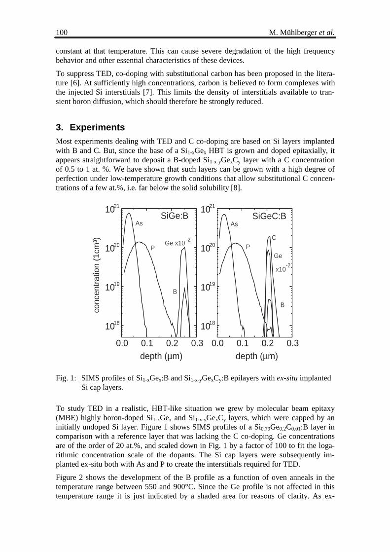
100 M. Mühlberger et al.
constant at that temperature. This can cause severe degradation of the high frequencybehavior and other essential characteristics of these devices.
To suppress TED, co-doping with substitutional carbon has been proposed in the litera-ture [6]. At sufficiently high concentrations, carbon is believed to form complexes withthe injected Si interstitials [7]. This limits the density of interstitials available to tran-sient boron diffusion, which should therefore be strongly reduced.
3. ExperimentsMost experiments dealing with TED and C co-doping are based on Si layers implantedwith B and C. But, since the base of a Si1-xGex HBT is grown and doped epitaxially, itappears straightforward to deposit a B-doped Si1-x-yGexCy layer with a C concentrationof 0.5 to 1 at. %. We have shown that such layers can be grown with a high degree ofperfection under low-temperature growth conditions that allow substitutional C concen-trations of a few at.%, i.e. far below the solid solubility [8].
0.0 0.1 0.2 0.3
1018
1019
1020
1021
SiGe:B
B
Ge x10 -2
P
As
depth (µm)0.0 0.1 0.2 0.3
1018
1019
1020
1021
Ge
x10-2
B
CP
AsSiGeC:B
depth (µm)
conc
entr
atio
n (1
cm³)
conc
entr
atio
n (1
cm³)
Fig. 1: SIMS profiles of Si1-xGex:B and Si1-x-yGexCy:B epilayers with ex-situ implantedSi cap layers.
To study TED in a realistic, HBT-like situation we grew by molecular beam epitaxy(MBE) highly boron-doped Si1-xGex and Si1-x-yGexCy layers, which were capped by aninitially undoped Si layer. Figure 1 shows SIMS profiles of a Si0.79Ge0.2C0.01:B layer incomparison with a reference layer that was lacking the C co-doping. Ge concentrationsare of the order of 20 at.%, and scaled down in Fig. 1 by a factor of 100 to fit the loga-rithmic concentration scale of the dopants. The Si cap layers were subsequently im-planted ex-situ both with As and P to create the interstitials required for TED.
Figure 2 shows the development of the B profile as a function of oven anneals in thetemperature range between 550 and 900°C. Since the Ge profile is not affected in thistemperature range it is just indicated by a shaded area for reasons of clarity. As ex-
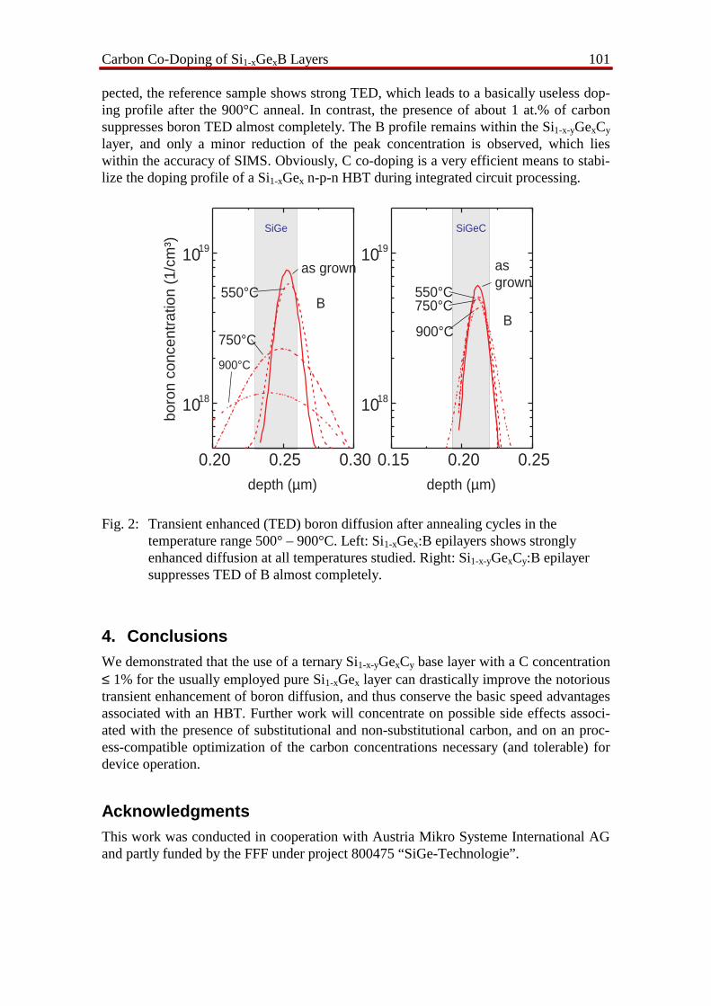
Carbon Co-Doping of Si1-xGexB Layers 101
pected, the reference sample shows strong TED, which leads to a basically useless dop-ing profile after the 900°C anneal. In contrast, the presence of about 1 at.% of carbonsuppresses boron TED almost completely. The B profile remains within the Si1-x-yGexCy
layer, and only a minor reduction of the peak concentration is observed, which lieswithin the accuracy of SIMS. Obviously, C co-doping is a very efficient means to stabi-lize the doping profile of a Si1-xGex n-p-n HBT during integrated circuit processing.
0.20 0.25 0.30
1018
1019
B
SiGe
900°C
750°C
550°C
as grown
depth (µm)
0.15 0.20 0.25
1018
1019
B900°C
750°C550°C
asgrown
SiGeC
depth (µm)
boro
n co
ncen
trat
ion
(1/c
m³)
boro
n co
ncen
trat
ion
(1/c
m³)
Fig. 2: Transient enhanced (TED) boron diffusion after annealing cycles in thetemperature range 500° – 900°C. Left: Si1-xGex:B epilayers shows stronglyenhanced diffusion at all temperatures studied. Right: Si1-x-yGexCy:B epilayersuppresses TED of B almost completely.
4. ConclusionsWe demonstrated that the use of a ternary Si1-x-yGexCy base layer with a C concentration≤ 1% for the usually employed pure Si1-xGex layer can drastically improve the notorioustransient enhancement of boron diffusion, and thus conserve the basic speed advantagesassociated with an HBT. Further work will concentrate on possible side effects associ-ated with the presence of substitutional and non-substitutional carbon, and on an proc-ess-compatible optimization of the carbon concentrations necessary (and tolerable) fordevice operation.
AcknowledgmentsThis work was conducted in cooperation with Austria Mikro Systeme International AGand partly funded by the FFF under project 800475 “SiGe-Technologie”.

102 M. Mühlberger et al.
References[1] B.S.Meyerson (IBM), Proc. MRS Fall Meeting 1998
[2] M.Schatzmayr (AMS), Proc. GMe Tagung, Hofgastein 1999, pp. 133-137
[3] D.L.Harame et al., IEDM Digest 1993, pp.71-74
[4] A.Gruhle et al., IEEE Electron. Dev. Lett. 13, 206-208 (1992)
[5] R.B.Fair, IEEE Trans. Electron. Dev. 35, 285 (1988)
[6] S.Nishikawa et al., Appl. Phys. Lett. 60, 2270-2272 (1992)
[7] N.E.B.Cowern et al., Appl. Phys. Lett. 68, 1150-1152 (1996)
[8] S.Zerlauth et al., Appl. Phys. Lett. 71, 3826-3828 (1997)
The Society for Microelectronics – Annual Report 1999 103
Modulation Doped Si/Si 1-xGex-Field-EffectTransistors
N. Sandersfeld, H. Seyringer, G. Steinbacher, L. Palmetshofer, S. Zerlauth,and F. Schäffler
Institut für Halbleiter- und Festkörperphysik,Johannes-Kepler-Universität Linz, A-4040 Linz
Modulation doped Si/Si1-xGex samples show high electron mobilities because of themotion of the carriers along a crystalline heterointerface and the absence of ionizedimpurities in the conduction channel. We present the methods and technologies thatare applied at our institute to fabricate field-effect transistors on MBE-grown modu-lation doped Si/Si1-xGex substrates. Ion implantation is used to form highly doped re-gions in the substrate; metal evaporation then realizes ohmic source and drain con-tacts on the implanted regions, and Schottky gates on unimplanted regions. In a fol-lowing mesa process, reactive ion etching (RIE) is used to isolate the devices on thesubstrate laterally. The complete transistor process requires six lithographic steps.We employ optical contact lithography for structures down to 0.5 µm and electron-beam lithography for gate lengths <0.5µm. By incorporation of a variety of teststructures in our process, we are able to derive the essential device and process pa-rameters after each technology step. For these characterizations we use an HP 4155semiconductor parameter analyzer and an HP 4284 LCR-meter in connection with anon-wafer prober.
1. IntroductionIn a modulation doped Si/Si1-xGex heterostructure, a 2-dimensional electron gas (2DEG)is formed which shows much higher mobilities than the 2DEG in a conventional SiO2/Siheterostructure [1]. This is for one due to the fact that the charge carriers move along acrystalline heterointerface instead of an amorphous one. In addition, by modulationdoping, the doping layer is spatially separated from the conduction channel, so freeelectrons are provided without having ionized impurities in the conduction path.
Our aim is to test the device applications of modulation doped Si/Si1-xGex heterostruc-tures grown by MBE at our institute. For this purpose we process several test structuresup to a modulation doped field-effect transistor (MODFET). These fabrication processesconsist of different technological steps [2] which have to be controlled and optimizedwith respect to the device and process parameters. In this outline we describe the tech-nological steps that are necessary, as well as the different test structures which we em-ploy to get information about our samples.
2. Technological BackgroundA field-effect transistor requires two kinds of contacts, nonrectifying ohmic contacts andwell rectifying Schottky contacts. For an ohmic metal-semiconductor contact, the semi-conductor has to be highly doped, so the charge carriers can tunnel through the Schottkybarrier. This doping procedure is done by ion implantation, where the ionized dopantsare accelerated toward the sample. The doping profile depth is then a function of the
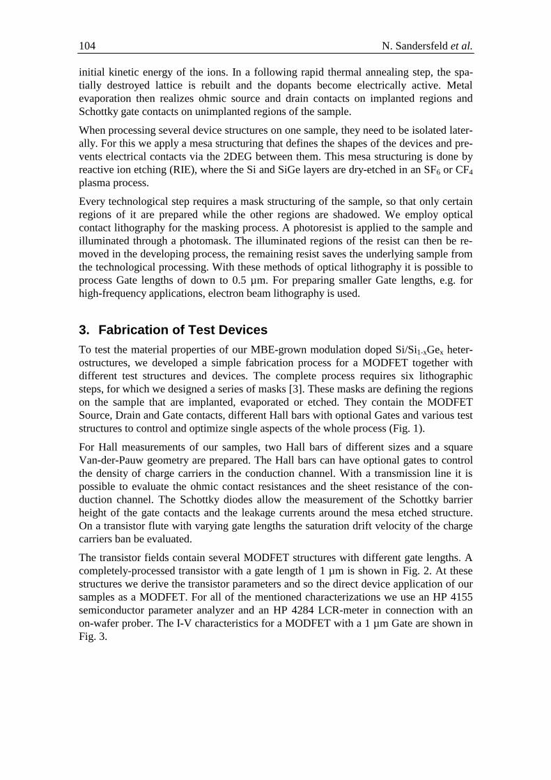
104 N. Sandersfeld et al.
initial kinetic energy of the ions. In a following rapid thermal annealing step, the spa-tially destroyed lattice is rebuilt and the dopants become electrically active. Metalevaporation then realizes ohmic source and drain contacts on implanted regions andSchottky gate contacts on unimplanted regions of the sample.
When processing several device structures on one sample, they need to be isolated later-ally. For this we apply a mesa structuring that defines the shapes of the devices and pre-vents electrical contacts via the 2DEG between them. This mesa structuring is done byreactive ion etching (RIE), where the Si and SiGe layers are dry-etched in an SF6 or CF4
plasma process.
Every technological step requires a mask structuring of the sample, so that only certainregions of it are prepared while the other regions are shadowed. We employ opticalcontact lithography for the masking process. A photoresist is applied to the sample andilluminated through a photomask. The illuminated regions of the resist can then be re-moved in the developing process, the remaining resist saves the underlying sample fromthe technological processing. With these methods of optical lithography it is possible toprocess Gate lengths of down to 0.5 µm. For preparing smaller Gate lengths, e.g. forhigh-frequency applications, electron beam lithography is used.
3. Fabrication of Test DevicesTo test the material properties of our MBE-grown modulation doped Si/Si1-xGex heter-ostructures, we developed a simple fabrication process for a MODFET together withdifferent test structures and devices. The complete process requires six lithographicsteps, for which we designed a series of masks [3]. These masks are defining the regionson the sample that are implanted, evaporated or etched. They contain the MODFETSource, Drain and Gate contacts, different Hall bars with optional Gates and various teststructures to control and optimize single aspects of the whole process (Fig. 1).
For Hall measurements of our samples, two Hall bars of different sizes and a squareVan-der-Pauw geometry are prepared. The Hall bars can have optional gates to controlthe density of charge carriers in the conduction channel. With a transmission line it ispossible to evaluate the ohmic contact resistances and the sheet resistance of the con-duction channel. The Schottky diodes allow the measurement of the Schottky barrierheight of the gate contacts and the leakage currents around the mesa etched structure.On a transistor flute with varying gate lengths the saturation drift velocity of the chargecarriers ban be evaluated.
The transistor fields contain several MODFET structures with different gate lengths. Acompletely-processed transistor with a gate length of 1 µm is shown in Fig. 2. At thesestructures we derive the transistor parameters and so the direct device application of oursamples as a MODFET. For all of the mentioned characterizations we use an HP 4155semiconductor parameter analyzer and an HP 4284 LCR-meter in connection with anon-wafer prober. The I-V characteristics for a MODFET with a 1 µm Gate are shown inFig. 3.
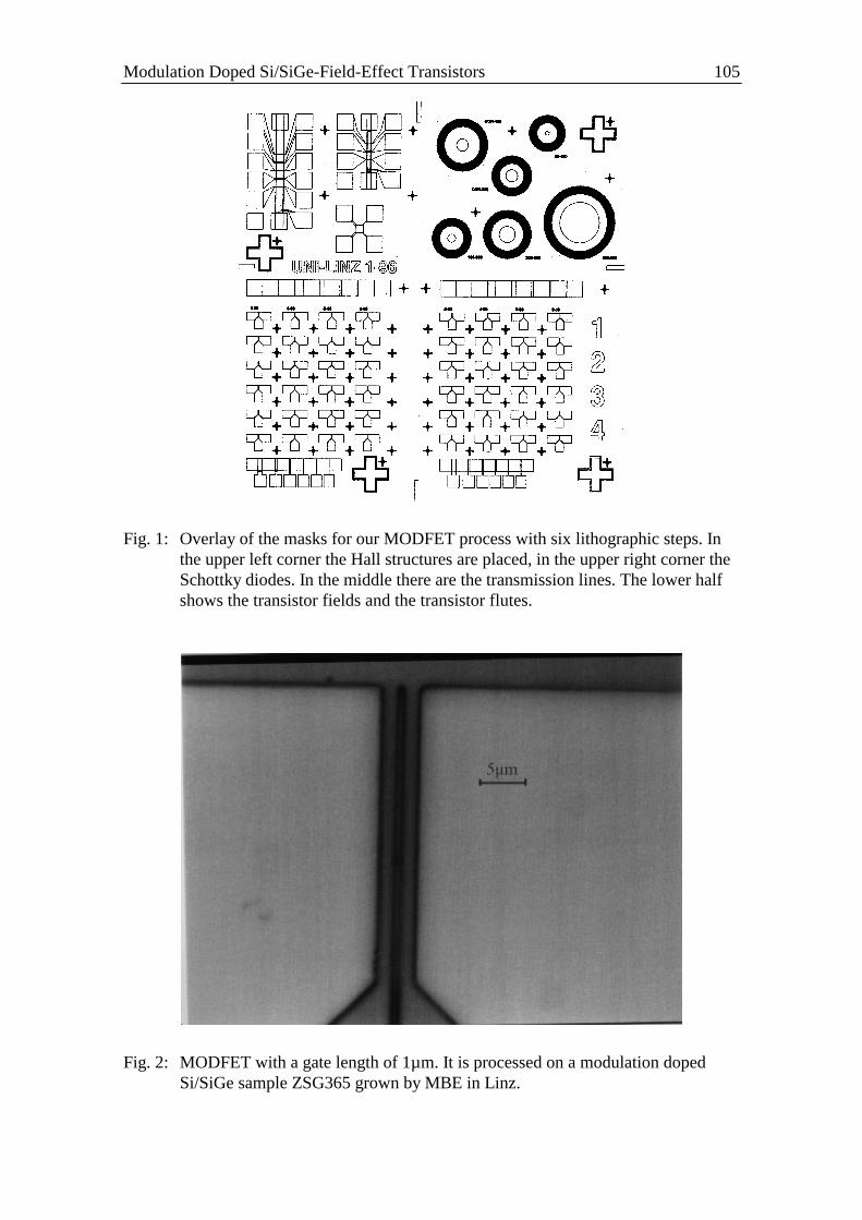
Modulation Doped Si/SiGe-Field-Effect Transistors 105
Fig. 1: Overlay of the masks for our MODFET process with six lithographic steps. Inthe upper left corner the Hall structures are placed, in the upper right corner theSchottky diodes. In the middle there are the transmission lines. The lower halfshows the transistor fields and the transistor flutes.
Fig. 2: MODFET with a gate length of 1µm. It is processed on a modulation dopedSi/SiGe sample ZSG365 grown by MBE in Linz.
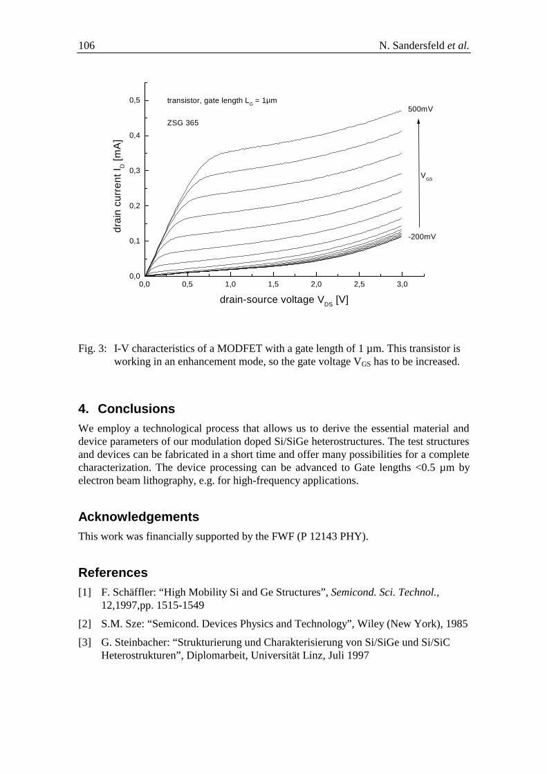
106 N. Sandersfeld et al.
0,0 0,5 1,0 1,5 2,0 2,5 3,00,0
0,1
0,2
0,3
0,4
0,5
VGS
500mV
-200mV
transistor, gate length LG = 1µm
ZSG 365dr
ain
curr
ent
I D [m
A]
drain-source voltage VDS
[V]
Fig. 3: I-V characteristics of a MODFET with a gate length of 1 µm. This transistor isworking in an enhancement mode, so the gate voltage VGS has to be increased.
4. ConclusionsWe employ a technological process that allows us to derive the essential material anddevice parameters of our modulation doped Si/SiGe heterostructures. The test structuresand devices can be fabricated in a short time and offer many possibilities for a completecharacterization. The device processing can be advanced to Gate lengths <0.5 µm byelectron beam lithography, e.g. for high-frequency applications.
AcknowledgementsThis work was financially supported by the FWF (P 12143 PHY).
References[1] F. Schäffler: “High Mobility Si and Ge Structures”, Semicond. Sci. Technol.,
12,1997,pp. 1515-1549
[2] S.M. Sze: “Semicond. Devices Physics and Technology”, Wiley (New York), 1985
[3] G. Steinbacher: “Strukturierung und Charakterisierung von Si/SiGe und Si/SiCHeterostrukturen”, Diplomarbeit, Universität Linz, Juli 1997
The Society for Microelectronics – Annual Report 1999 107
Growth Instabilities in Si HomoepitaxyC. Schelling, G. Springholz, F. Schäffler
Institut für Halbleiterphysik,Johannes-Kepler-Universität Linz, A-4040 Linz
We report on a new type of growth instability in Si homoepitaxy that arises from aslight sample miscut. This instability leads to a considerable surface roughness of upto 20 Å on a distance of 250 nm and occurs in a temperature regime frequently usedfor Si buffer growth. We also provide a recipe to avoid surface roughening.
1. IntroductionThe technical relevance of Si (001) surfaces and interfaces caused strong interest andintensive research efforts in their growth properties. The Si surface shows a general ten-dency for roughening during strained layer heteroepitaxy. Recently, some groups in-vestigate this phenomenon that is commonly known as step bunching and try to amplifyit to obtain templates for lateral ordering in subsequent self-organized growth, such ase.g. Ge islands.
The electronic properties of layers resulting from overgrowth are strongly influenced bytheir interface morphology as carrier scattering from interfacial roughness plays a majorrole for transport in heterostructure devices. Therefore, ideally flat Si and SiGe inter-faces are indispensable prerequisites for optimum performance in present and future Si-based heterostructure devices. It is the goal of our work here to investigate the involvedroughening mechanisms on the Si [001] surface and understand their driving forces toallow for the fabrication of interfaces that are as flat as possible and thus ideal for het-erostructure devices.
2. Experiment
2.1 Experimental
The samples used for this study were cut from standard Si (001) wafers into 17×17 mmpieces. The substrates have well-defined miscuts of some 1° and 2° along the [100] and1,5° along the [110] direction, respectively. We used an HF-free standard RCA cleaningprocedure before loading them into our Riber SIVA 45 MBE machine. An oxide de-sorption step at 1000 °C initiates subsequent overgrowth. Si and SiGe layers were de-posited at growth rates of 0,2 and 0,8 Å/s and growth temperatures between 350 °C and750 °C, the layer thickness usually being 1000 Å.
After growth the surface morphology was immediately mapped in ambient air with aPark Scientific atomic force microscope (AFM) in contact mode.
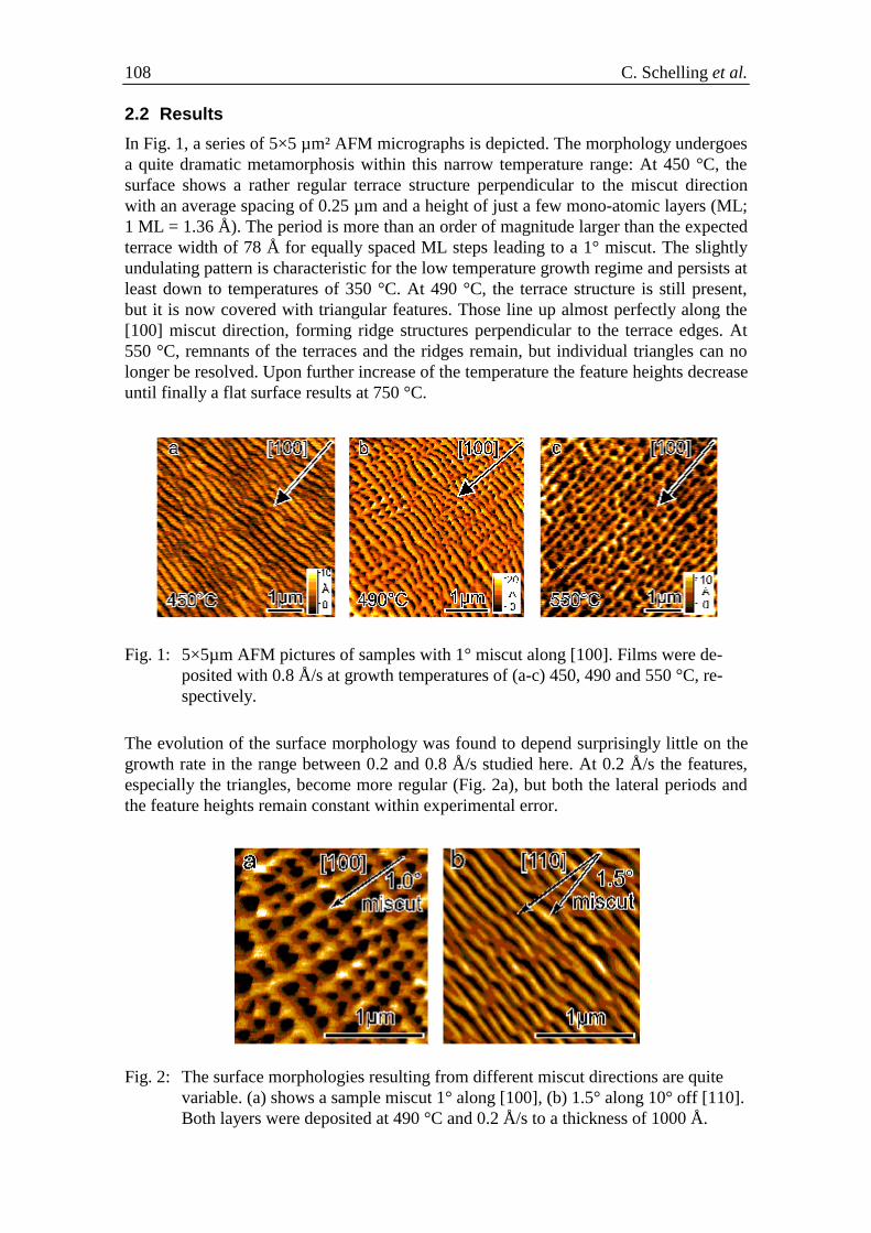
108 C. Schelling et al.
2.2 Results
In Fig. 1, a series of 5×5 µm² AFM micrographs is depicted. The morphology undergoesa quite dramatic metamorphosis within this narrow temperature range: At 450 °C, thesurface shows a rather regular terrace structure perpendicular to the miscut directionwith an average spacing of 0.25 µm and a height of just a few mono-atomic layers (ML;1 ML = 1.36 Å). The period is more than an order of magnitude larger than the expectedterrace width of 78 Å for equally spaced ML steps leading to a 1° miscut. The slightlyundulating pattern is characteristic for the low temperature growth regime and persists atleast down to temperatures of 350 °C. At 490 °C, the terrace structure is still present,but it is now covered with triangular features. Those line up almost perfectly along the[100] miscut direction, forming ridge structures perpendicular to the terrace edges. At550 °C, remnants of the terraces and the ridges remain, but individual triangles can nolonger be resolved. Upon further increase of the temperature the feature heights decreaseuntil finally a flat surface results at 750 °C.
Fig. 1: 5×5µm AFM pictures of samples with 1° miscut along [100]. Films were de-posited with 0.8 Å/s at growth temperatures of (a-c) 450, 490 and 550 °C, re-spectively.
The evolution of the surface morphology was found to depend surprisingly little on thegrowth rate in the range between 0.2 and 0.8 Å/s studied here. At 0.2 Å/s the features,especially the triangles, become more regular (Fig. 2a), but both the lateral periods andthe feature heights remain constant within experimental error.
Fig. 2: The surface morphologies resulting from different miscut directions are quitevariable. (a) shows a sample miscut 1° along [100], (b) 1.5° along 10° off [110].Both layers were deposited at 490 °C and 0.2 Å/s to a thickness of 1000 Å.
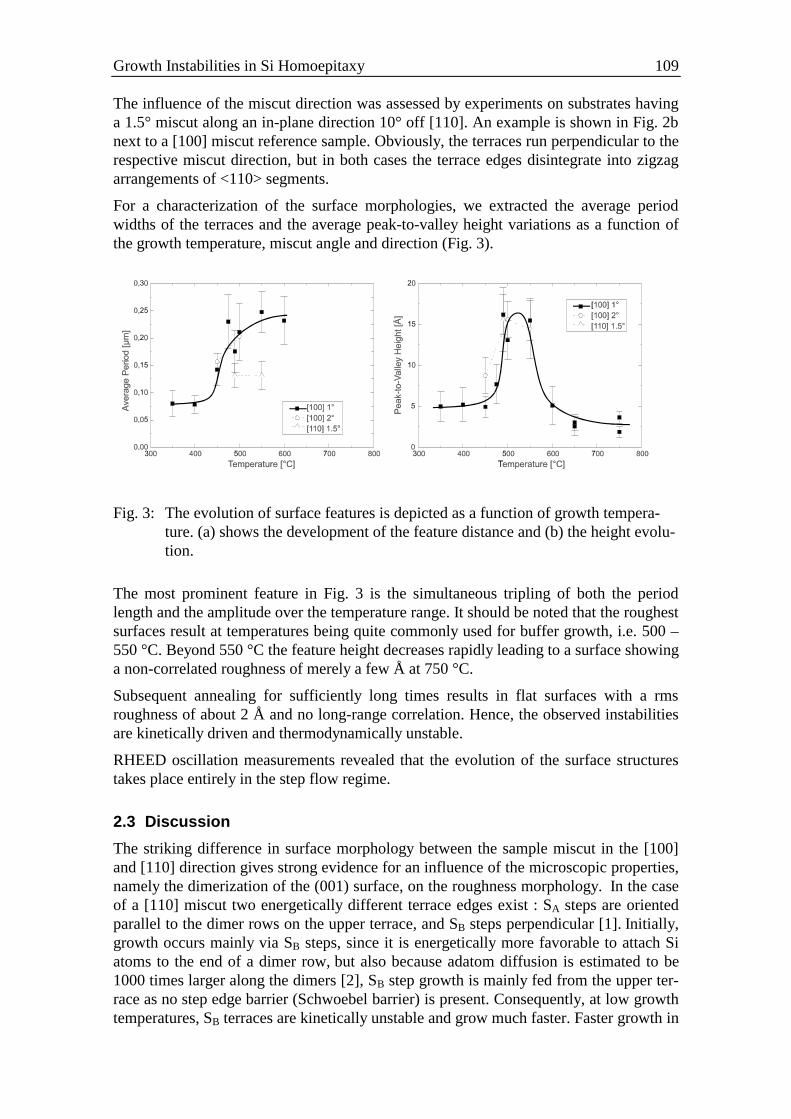
Growth Instabilities in Si Homoepitaxy 109
The influence of the miscut direction was assessed by experiments on substrates havinga 1.5° miscut along an in-plane direction 10° off [110]. An example is shown in Fig. 2bnext to a [100] miscut reference sample. Obviously, the terraces run perpendicular to therespective miscut direction, but in both cases the terrace edges disintegrate into zigzagarrangements of <110> segments.
For a characterization of the surface morphologies, we extracted the average periodwidths of the terraces and the average peak-to-valley height variations as a function ofthe growth temperature, miscut angle and direction (Fig. 3).
Fig. 3: The evolution of surface features is depicted as a function of growth tempera-ture. (a) shows the development of the feature distance and (b) the height evolu-tion.
The most prominent feature in Fig. 3 is the simultaneous tripling of both the periodlength and the amplitude over the temperature range. It should be noted that the roughestsurfaces result at temperatures being quite commonly used for buffer growth, i.e. 500 –550 °C. Beyond 550 °C the feature height decreases rapidly leading to a surface showinga non-correlated roughness of merely a few Å at 750 °C.
Subsequent annealing for sufficiently long times results in flat surfaces with a rmsroughness of about 2 Å and no long-range correlation. Hence, the observed instabilitiesare kinetically driven and thermodynamically unstable.
RHEED oscillation measurements revealed that the evolution of the surface structurestakes place entirely in the step flow regime.
2.3 Discussion
The striking difference in surface morphology between the sample miscut in the [100]and [110] direction gives strong evidence for an influence of the microscopic properties,namely the dimerization of the (001) surface, on the roughness morphology. In the caseof a [110] miscut two energetically different terrace edges exist : SA steps are orientedparallel to the dimer rows on the upper terrace, and SB steps perpendicular [1]. Initially,growth occurs mainly via SB steps, since it is energetically more favorable to attach Siatoms to the end of a dimer row, but also because adatom diffusion is estimated to be1000 times larger along the dimers [2], SB step growth is mainly fed from the upper ter-race as no step edge barrier (Schwoebel barrier) is present. Consequently, at low growthtemperatures, SB terraces are kinetically unstable and grow much faster. Faster growth in
110 C. Schelling et al.
return leads to a larger upper terraces, which again means a larger capture ratio, as com-pared to SA type steps. In the end, this instability generally leads to step bunching andrough surfaces (see fig 2b). At somewhat higher temperatures, however, the diffusionperpendicular to the dimer rows becomes enhanced and finally the predominant diffu-sion asymmetry observed at lower temperatures is overcome, SA steps advance as fast asSB steps and the result is a flat surface.
The behavior of the [100] miscut samples is far more complex and not yet fully under-stood. The <110> segmentation can be understood as caused by “diffusion trenches”along the step edges, where diffusion barriers might be lower and adatoms are highlymobile. The almost perfect alignment of the triangles could be explained in terms ofstrain fields that are known to be connected with the surface dimer rows.
3. ConclusionsConsidering the fact that every wafer is usually specified only within ±0,5° of an exactcrystal plane the outcome of our experiments bears important implications for Si-basedepitaxy. They clearly show that one has to be very concerned about Si buffer growth.Investigations on strain-induced step bunching should be carried out quite carefully.Bearing in mind that HF cleaned wafers cannot be overgrown at high temperatures be-cause of the formation of SiC precipitates and as a consequence thereof the evolution ofa considerable surface roughness. This leaves us in principal with two alternatives : FlatSi buffers on an HF cleaned wafer by either two successive buffer layers the first grownat a low temperature to avoid SiC precipitates to be formed and a second grown athigher temperatures above 600°C to smoothen the surface afterwards or annealing of thesubstrates after buffer growth. The second viable way to achieve a flat surface is to useRCA cleaned wafers. RCA cleaning leaves a nearly C-free oxidized wafer surface thatthus can be overgrown with a Si buffer at temperatures above 650°C. This approachprovides the surfaces best suited for heterostructure devices as well as future surfaceinvestigations.
AcknowledgementsWe would like to thank J. Vanhellemont (Wacker Siltronic) and K. Brunner (WSI Mu-nich) for providing the substrates and J. Stangl for some X-ray measurements. We arealso grateful for discussions with G. Bauer and B. Voigtländer. This work was finan-cially supported by FWF (Project 12143 PHY), OeNB (Project 7333)
References[1] B.S.Swartzentruber, Y.-W.Mo, R.Kariotis, M.G.Lagally, and M.B.Webb : “Direct
Determination of Step and Kink Energies on Vicinal Si(001)”, Phys. Rev. Lett.,Vol. 65, 1990, pp. 1913 – 191
[2] Y.-W. Mo and M. Lagally : “Anisotropy in surface migration of Si and Ge onSi(001)”, Surf. Sci., Vol. 248, 1991, pp. 313 – 319
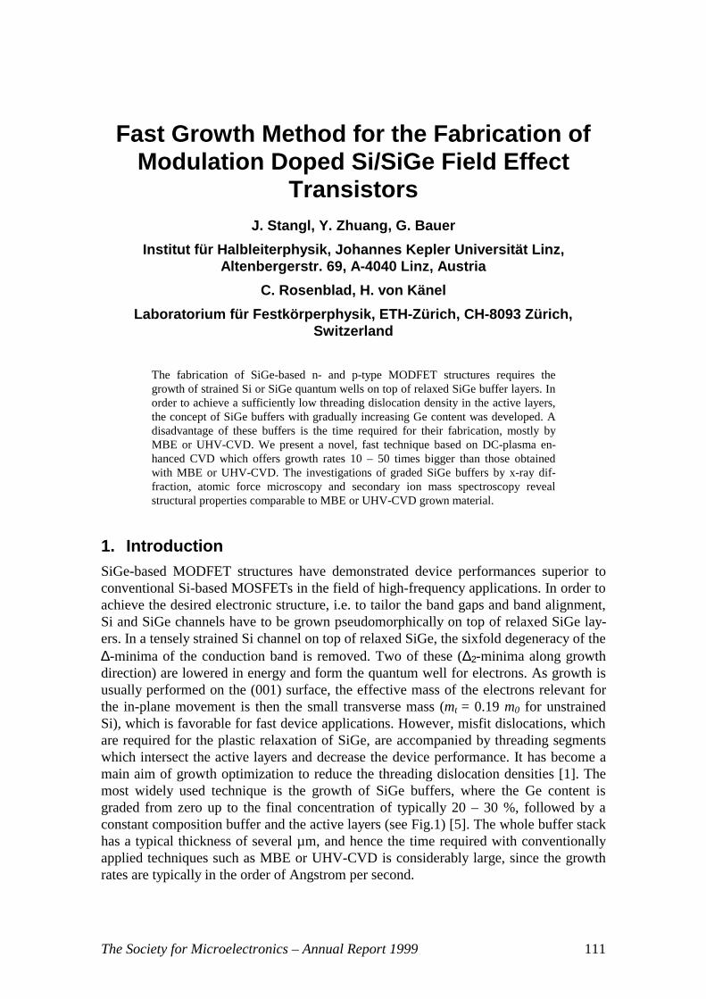
The Society for Microelectronics – Annual Report 1999 111
Fast Growth Method for the Fabrication ofModulation Doped Si/SiGe Field Effect
TransistorsJ. Stangl, Y. Zhuang, G. Bauer
Institut für Halbleiterphysik, Johannes Kepler Universität Linz,Altenbergerstr. 69, A-4040 Linz, Austria
C. Rosenblad, H. von Känel
Laboratorium für Festkörperphysik, ETH-Zürich, CH-8093 Zürich,Switzerland
The fabrication of SiGe-based n- and p-type MODFET structures requires thegrowth of strained Si or SiGe quantum wells on top of relaxed SiGe buffer layers. Inorder to achieve a sufficiently low threading dislocation density in the active layers,the concept of SiGe buffers with gradually increasing Ge content was developed. Adisadvantage of these buffers is the time required for their fabrication, mostly byMBE or UHV-CVD. We present a novel, fast technique based on DC-plasma en-hanced CVD which offers growth rates 10 – 50 times bigger than those obtainedwith MBE or UHV-CVD. The investigations of graded SiGe buffers by x-ray dif-fraction, atomic force microscopy and secondary ion mass spectroscopy revealstructural properties comparable to MBE or UHV-CVD grown material.
1. IntroductionSiGe-based MODFET structures have demonstrated device performances superior toconventional Si-based MOSFETs in the field of high-frequency applications. In order toachieve the desired electronic structure, i.e. to tailor the band gaps and band alignment,Si and SiGe channels have to be grown pseudomorphically on top of relaxed SiGe lay-ers. In a tensely strained Si channel on top of relaxed SiGe, the sixfold degeneracy of the∆-minima of the conduction band is removed. Two of these (∆2-minima along growthdirection) are lowered in energy and form the quantum well for electrons. As growth isusually performed on the (001) surface, the effective mass of the electrons relevant forthe in-plane movement is then the small transverse mass (mt = 0.19 m0 for unstrainedSi), which is favorable for fast device applications. However, misfit dislocations, whichare required for the plastic relaxation of SiGe, are accompanied by threading segmentswhich intersect the active layers and decrease the device performance. It has become amain aim of growth optimization to reduce the threading dislocation densities [1]. Themost widely used technique is the growth of SiGe buffers, where the Ge content isgraded from zero up to the final concentration of typically 20 – 30 %, followed by aconstant composition buffer and the active layers (see Fig.1) [5]. The whole buffer stackhas a typical thickness of several µm, and hence the time required with conventionallyapplied techniques such as MBE or UHV-CVD is considerably large, since the growthrates are typically in the order of Angstrom per second.
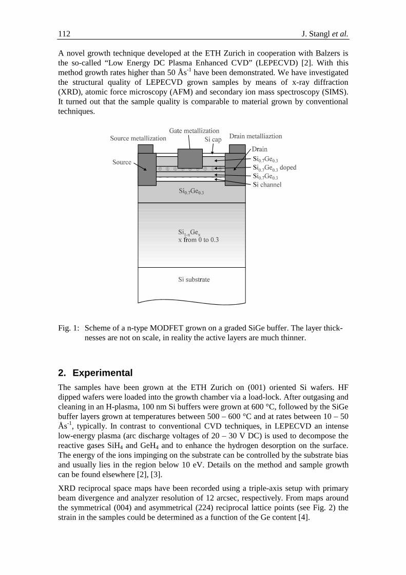
112 J. Stangl et al.
A novel growth technique developed at the ETH Zurich in cooperation with Balzers isthe so-called “Low Energy DC Plasma Enhanced CVD” (LEPECVD) [2]. With thismethod growth rates higher than 50 Ås-1 have been demonstrated. We have investigatedthe structural quality of LEPECVD grown samples by means of x-ray diffraction(XRD), atomic force microscopy (AFM) and secondary ion mass spectroscopy (SIMS).It turned out that the sample quality is comparable to material grown by conventionaltechniques.
Fig. 1: Scheme of a n-type MODFET grown on a graded SiGe buffer. The layer thick-nesses are not on scale, in reality the active layers are much thinner.
2. ExperimentalThe samples have been grown at the ETH Zurich on (001) oriented Si wafers. HFdipped wafers were loaded into the growth chamber via a load-lock. After outgasing andcleaning in an H-plasma, 100 nm Si buffers were grown at 600 °C, followed by the SiGebuffer layers grown at temperatures between 500 – 600 °C and at rates between 10 – 50Ås-1, typically. In contrast to conventional CVD techniques, in LEPECVD an intenselow-energy plasma (arc discharge voltages of 20 – 30 V DC) is used to decompose thereactive gases SiH4 and GeH4 and to enhance the hydrogen desorption on the surface.The energy of the ions impinging on the substrate can be controlled by the substrate biasand usually lies in the region below 10 eV. Details on the method and sample growthcan be found elsewhere [2], [3].
XRD reciprocal space maps have been recorded using a triple-axis setup with primarybeam divergence and analyzer resolution of 12 arcsec, respectively. From maps aroundthe symmetrical (004) and asymmetrical (224) reciprocal lattice points (see Fig. 2) thestrain in the samples could be determined as a function of the Ge content [4].
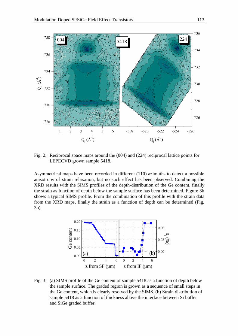
Modulation Doped Si/SiGe Field Effect Transistors 113
Fig. 2: Reciprocal space maps around the (004) and (224) reciprocal lattice points forLEPECVD grown sample 5418.
Asymmetrical maps have been recorded in different (110) azimuths to detect a possibleanisotropy of strain relaxation, but no such effect has been observed. Combining theXRD results with the SIMS profiles of the depth-distribution of the Ge content, finallythe strain as function of depth below the sample surface has been determined. Figure 3bshows a typical SIMS profile. From the combination of this profile with the strain datafrom the XRD maps, finally the strain as a function of depth can be determined (Fig.3b).
0 2 4 6
0.00
0.03
0.06
(b)
ε|| (%
)
z from IF (µm)0 2 4 6
0.00
0.05
0.10
0.15
0.20
(a)
z from SF (µm)
Ge
cont
ent
Fig. 3: (a) SIMS profile of the Ge content of sample 5418 as a function of depth belowthe sample surface. The graded region is grown as a sequence of small steps inthe Ge content, which is clearly resolved by the SIMS. (b) Strain distribution ofsample 5418 as a function of thickness above the interface between Si bufferand SiGe graded buffer.
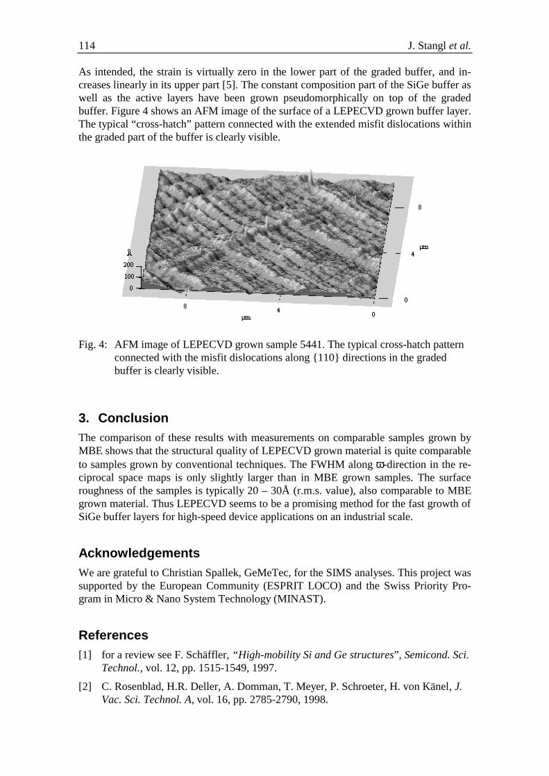
114 J. Stangl et al.
As intended, the strain is virtually zero in the lower part of the graded buffer, and in-creases linearly in its upper part [5]. The constant composition part of the SiGe buffer aswell as the active layers have been grown pseudomorphically on top of the gradedbuffer. Figure 4 shows an AFM image of the surface of a LEPECVD grown buffer layer.The typical “cross-hatch” pattern connected with the extended misfit dislocations withinthe graded part of the buffer is clearly visible.
Fig. 4: AFM image of LEPECVD grown sample 5441. The typical cross-hatch patternconnected with the misfit dislocations along 110 directions in the gradedbuffer is clearly visible.
3. ConclusionThe comparison of these results with measurements on comparable samples grown byMBE shows that the structural quality of LEPECVD grown material is quite comparableto samples grown by conventional techniques. The FWHM along ω-direction in the re-ciprocal space maps is only slightly larger than in MBE grown samples. The surfaceroughness of the samples is typically 20 – 30Å (r.m.s. value), also comparable to MBEgrown material. Thus LEPECVD seems to be a promising method for the fast growth ofSiGe buffer layers for high-speed device applications on an industrial scale.
AcknowledgementsWe are grateful to Christian Spallek, GeMeTec, for the SIMS analyses. This project wassupported by the European Community (ESPRIT LOCO) and the Swiss Priority Pro-gram in Micro & Nano System Technology (MINAST).
References[1] for a review see F. Schäffler, “High-mobility Si and Ge structures”, Semicond. Sci.
Technol., vol. 12, pp. 1515-1549, 1997.
[2] C. Rosenblad, H.R. Deller, A. Domman, T. Meyer, P. Schroeter, H. von Känel, J.Vac. Sci. Technol. A, vol. 16, pp. 2785-2790, 1998.

Modulation Doped Si/SiGe Field Effect Transistors 115
[3] C. Rosenblad, H.R. Deller, H. von Känel, Thin Solid Films, vol. 378, pp. 89-91,1998.
[4] J.H. Li, V. Holý, G. Bauer, F. Schäffler, J. Appl. Phys., vol. 82, pp. 2881-2886,1997.
[5] J. Tersoff, Appl. Phys. Lett., vol. 62, pp. 693-695, 1993.

The Society for Microelectronics – Annual Report 1999 117
Si/SiGe Layers on Patterned Substrates forMODFET Applications
Y. Zhuang, P. Mikulik, V. Holý, G. Bauer
Institut für Halbleiterphysik, Johannes Kepler Universität Linz, Austria
R. Hammond, T. E. Whall, E. H. C. Parker
Department of Physics, University of Warwick, Coventry, England
We present a systematic study on the strain status of Si channel in Si/SiGe MODFETstructures grown on mesa structures with lateral dimensions ranging from 3 to20 µm, as well of its surface morphology. With decreasing mesa size, the surface un-dulations flatten and the in-plane strain of the Si channel is decreased.
1. IntroductionIn Si-channel n-MODFET structures, a two dimensional electron gas is confined in astrained about 100 Å thick Si layer [1]. For tensile strain, the six-fold degenerate con-duction band of Si is split into a two-fold ∆2 and a fourfold ∆4 state. The confining po-tential for the electrons in this Si-channel layer is determined by the conduction bandoffset between the SiGe barrier and the ∆2 states of strained Si. In order to achieve thedesired strain status, usually a graded SiGe buffer layer is deposited on (001) Si, on topof which a constant composition SiGe layer is deposited, followed by the Si channel andfinally a modulation doped SiGe layer on top. The grading rate of the Ge content, thethickness of the graded layer (B1) and of the constant composition buffer (B2, see Fig.1)determine the amount of strain relaxation and thus the in-plane lattice constant of thetop B2 SiGe layer. The subsequently grown Si channel is pseudomorphic, i.e. biaxiallytensily strained with respect to buffer B2. The plastic relaxation of the SiGe buffer layeris through misfit dislocations, the stress fields of which give rise to the roughening ofthe epilayer and consequently also of the interface to the strained Si layer [1], [2] . Theresulting cross-hatch surface or interface morphology has a lateral periodicity of typi-cally 1 µm in the two orthogonal <110> directions, with rms heights of about 20 – 50 Å[2]. Too high values of this surface roughening might be not fully compatible with pla-nar integrated circuit technology.
A concept for Si-based heterostructure devices has been developed, in which such de-vices could be integrated with conventional Si MOS technology on the same wafer(chip) by growing the layer sequence for heterostructure in selected areas. However, thequality of these devices always suffered from the high density of defects induced by thelarge lattice mismatch between Si and Ge. It has been found that reducing the lateraldimensions of the growth zone results to a dramatic decrease in the defect densities [3].In this paper we describe a systematic study both of the strain status of the Si layer con-taining the 2D electron gas and of the surface morphology as a function of the lateraldimensions.
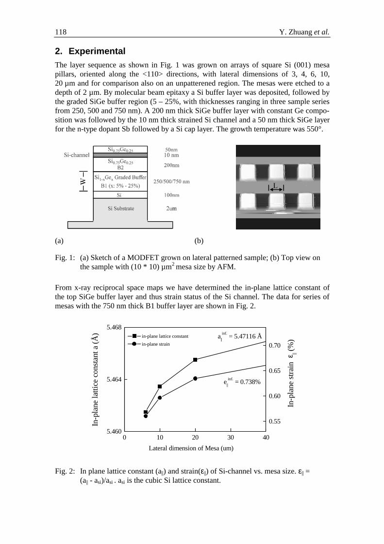
118 Y. Zhuang et al.
2. ExperimentalThe layer sequence as shown in Fig. 1 was grown on arrays of square Si (001) mesapillars, oriented along the <110> directions, with lateral dimensions of 3, 4, 6, 10,20 µm and for comparison also on an unpatterened region. The mesas were etched to adepth of 2 µm. By molecular beam epitaxy a Si buffer layer was deposited, followed bythe graded SiGe buffer region (5 – 25%, with thicknesses ranging in three sample seriesfrom 250, 500 and 750 nm). A 200 nm thick SiGe buffer layer with constant Ge compo-sition was followed by the 10 nm thick strained Si channel and a 50 nm thick SiGe layerfor the n-type dopant Sb followed by a Si cap layer. The growth temperature was 550°.
(a) (b)
Fig. 1: (a) Sketch of a MODFET grown on lateral patterned sample; (b) Top view onthe sample with (10 * 10) µm2 mesa size by AFM.
From x-ray reciprocal space maps we have determined the in-plane lattice constant ofthe top SiGe buffer layer and thus strain status of the Si channel. The data for series ofmesas with the 750 nm thick B1 buffer layer are shown in Fig. 2.
5.460
5.464
5.468
e||
inf. = 0.738%
a||
inf. = 5.47116 Å
In-p
lane
str
ain
ε || (%
) in-plane lattice constant
In-p
lane
latti
ce c
onst
ant a
(Å
)
Lateral dimension of Mesa (um)
0 10 20 30 40
0.55
0.60
0.65
0.70 in-plane strain
Fig. 2: In plane lattice constant (a||) and strain(ε||) of Si-channel vs. mesa size. ε|| =(a|| - asi)/asi . asi is the cubic Si lattice constant.
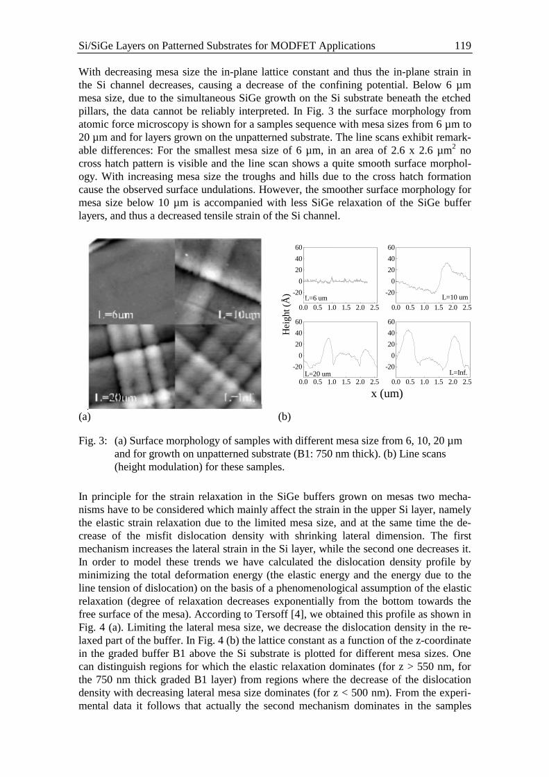
Si/SiGe Layers on Patterned Substrates for MODFET Applications 119
With decreasing mesa size the in-plane lattice constant and thus the in-plane strain inthe Si channel decreases, causing a decrease of the confining potential. Below 6 µmmesa size, due to the simultaneous SiGe growth on the Si substrate beneath the etchedpillars, the data cannot be reliably interpreted. In Fig. 3 the surface morphology fromatomic force microscopy is shown for a samples sequence with mesa sizes from 6 µm to20 µm and for layers grown on the unpatterned substrate. The line scans exhibit remark-able differences: For the smallest mesa size of 6 µm, in an area of 2.6 x 2.6 µm2 nocross hatch pattern is visible and the line scan shows a quite smooth surface morphol-ogy. With increasing mesa size the troughs and hills due to the cross hatch formationcause the observed surface undulations. However, the smoother surface morphology formesa size below 10 µm is accompanied with less SiGe relaxation of the SiGe bufferlayers, and thus a decreased tensile strain of the Si channel.
0.0 0.5 1.0 1.5 2.0 2.5
-20
0
20
40
60
L=6 um
x (um)
He
ight
(Å
)
0.0 0.5 1.0 1.5 2.0 2.5
-20
0
20
40
60
10 um
20 um Inf.
6 um L=10 um
0.0 0.5 1.0 1.5 2.0 2.5
-20
0
20
40
60
L=20 um0.0 0.5 1.0 1.5 2.0 2.5
-20
0
20
40
60
L=Inf.
(a) (b)
Fig. 3: (a) Surface morphology of samples with different mesa size from 6, 10, 20 µmand for growth on unpatterned substrate (B1: 750 nm thick). (b) Line scans(height modulation) for these samples.
In principle for the strain relaxation in the SiGe buffers grown on mesas two mecha-nisms have to be considered which mainly affect the strain in the upper Si layer, namelythe elastic strain relaxation due to the limited mesa size, and at the same time the de-crease of the misfit dislocation density with shrinking lateral dimension. The firstmechanism increases the lateral strain in the Si layer, while the second one decreases it.In order to model these trends we have calculated the dislocation density profile byminimizing the total deformation energy (the elastic energy and the energy due to theline tension of dislocation) on the basis of a phenomenological assumption of the elasticrelaxation (degree of relaxation decreases exponentially from the bottom towards thefree surface of the mesa). According to Tersoff [4], we obtained this profile as shown inFig. 4 (a). Limiting the lateral mesa size, we decrease the dislocation density in the re-laxed part of the buffer. In Fig. 4 (b) the lattice constant as a function of the z-coordinatein the graded buffer B1 above the Si substrate is plotted for different mesa sizes. Onecan distinguish regions for which the elastic relaxation dominates (for z > 550 nm, forthe 750 nm thick graded B1 layer) from regions where the decrease of the dislocationdensity with decreasing lateral mesa size dominates (for z < 500 nm). From the experi-mental data it follows that actually the second mechanism dominates in the samples
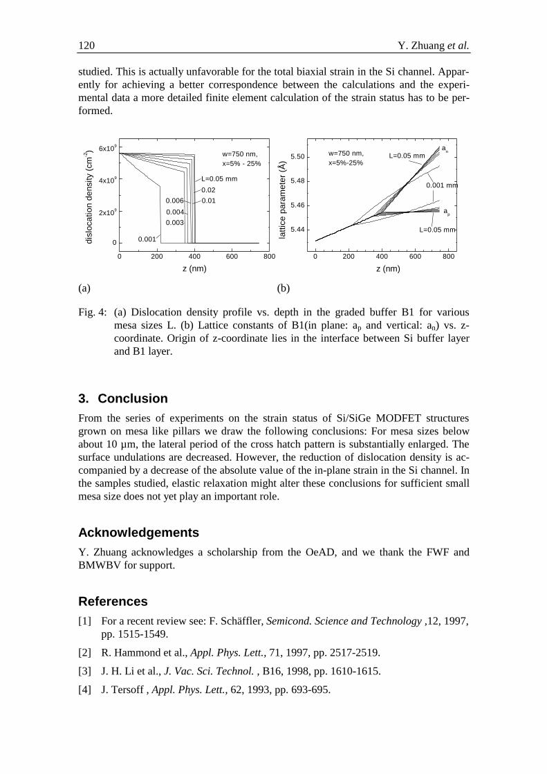
120 Y. Zhuang et al.
studied. This is actually unfavorable for the total biaxial strain in the Si channel. Appar-ently for achieving a better correspondence between the calculations and the experi-mental data a more detailed finite element calculation of the strain status has to be per-formed.
0 200 400 600 800
0
2x10⁹
4x10⁹
6x10⁹
0.001
0.003
0.004
0.006 0.01
0.02
L=0.05 mm
w=750 nm, x=5% - 25%
disl
ocat
ion
dens
ity (
cm-2)
z (nm)
0 200 400 600 800
5.44
5.46
5.48
5.50
ap
an
L=0.05 mm
0.001 mm
z (nm)
latti
ce p
aram
eter
(Å
)
L=0.05 mmw=750 nm,x=5%-25%
(a) (b)
Fig. 4: (a) Dislocation density profile vs. depth in the graded buffer B1 for variousmesa sizes L. (b) Lattice constants of B1(in plane: ap and vertical: an) vs. z-coordinate. Origin of z-coordinate lies in the interface between Si buffer layerand B1 layer.
3. ConclusionFrom the series of experiments on the strain status of Si/SiGe MODFET structuresgrown on mesa like pillars we draw the following conclusions: For mesa sizes belowabout 10 µm, the lateral period of the cross hatch pattern is substantially enlarged. Thesurface undulations are decreased. However, the reduction of dislocation density is ac-companied by a decrease of the absolute value of the in-plane strain in the Si channel. Inthe samples studied, elastic relaxation might alter these conclusions for sufficient smallmesa size does not yet play an important role.
AcknowledgementsY. Zhuang acknowledges a scholarship from the OeAD, and we thank the FWF andBMWBV for support.
References[1] For a recent review see: F. Schäffler, Semicond. Science and Technology ,12, 1997,
pp. 1515-1549.
[2] R. Hammond et al., Appl. Phys. Lett., 71, 1997, pp. 2517-2519.
[3] J. H. Li et al., J. Vac. Sci. Technol. , B16, 1998, pp. 1610-1615.
[4] J. Tersoff , Appl. Phys. Lett., 62, 1993, pp. 693-695.
The Society for Microelectronics – Annual Report 1999 121
Electron Beam Lithography ofNanostructures
H. Seyringer, B. Fünfstück, F. Schäffler
Institut für Halbleiterphysik, Uni LinzAltenbergerstr. 69, 4040-Linz
After a short description of the hard- and software we have used for making the na-nostructures, we report on three activities: i) For Si/SiGe modulation-doped field-effect transistors, we fabricate Schottky gates by a lift-off technique with gate lengthsbelow 100 nm. ii) By exposing arrays of boxes with a side length of less than 70 nmand by transferring them via reactive ion etching into a pre-structured Hall bar weproduced antidots for magnetotransport investigations. iii) Oxide-patterned siliconsubstrates are used as a template for selective molecular beam epitaxy. By combiningthe prepatterned substrates with Stranski-Krastanov growth of Ge or SiGe layers,self-organized quantum dots can be arranged in a regular pattern for selective exci-tation or contacting.
1. IntroductionFor electron beam lithography of nanostructures on Si/SiGe heterostructures we use aJEOL JSM 6400 scanning electron microscope at an accelerating voltage of 40 keV andPolymethylmetacrylat (PMMA) resists with molecular weights between 50k and 950ka.u. The samples are cleaned in acetone and methanol in combination with ultrasonic.On samples with no oxide layer we have used additionally a HF dip to increase the ad-hesion between substrate and photoresist. Beside the HF dip we have used no otherchemicals (like hexamethyldisilicane) to improve the adhesion between substrate andphotoresist.
To create the masks and for exposure we have used “Elphy FE 1.233D” from Raith.After a short trial period we have realized some bugs in the “Elphy FE” software whichmade it necessary to program at least a part of the software by ourselves. The “Nanoli-thography” package, we have programmed as a supplement for the “Elphy FE” softwareincludes a design part which allows to generate the masks and export them to “ElphyFE”. This solved the problem with instabilities in the mask design part of “Elphy FE”.To improve the exposure quality of periodic dot structures we have implemented a smallutility which optimizes the exposure parameters.
As a part of this optimization “Nanolithography” finds the proper combination ofworking area, working distance and magnification based on databases which include allthe technical parameters of the JSM 6400. This optimization takes also into account thatthe JEOL has only some discrete magnifications and working distances. Without theseroutines “Elphy FE” would expose either to small or to big structures.
The calibration of the scaling routines has been done with the help of a Park Scientificatomic force microscope. First we calibrated it with a gold grating of known period.After calibration we investigated a grating, which we had exposed with our electron
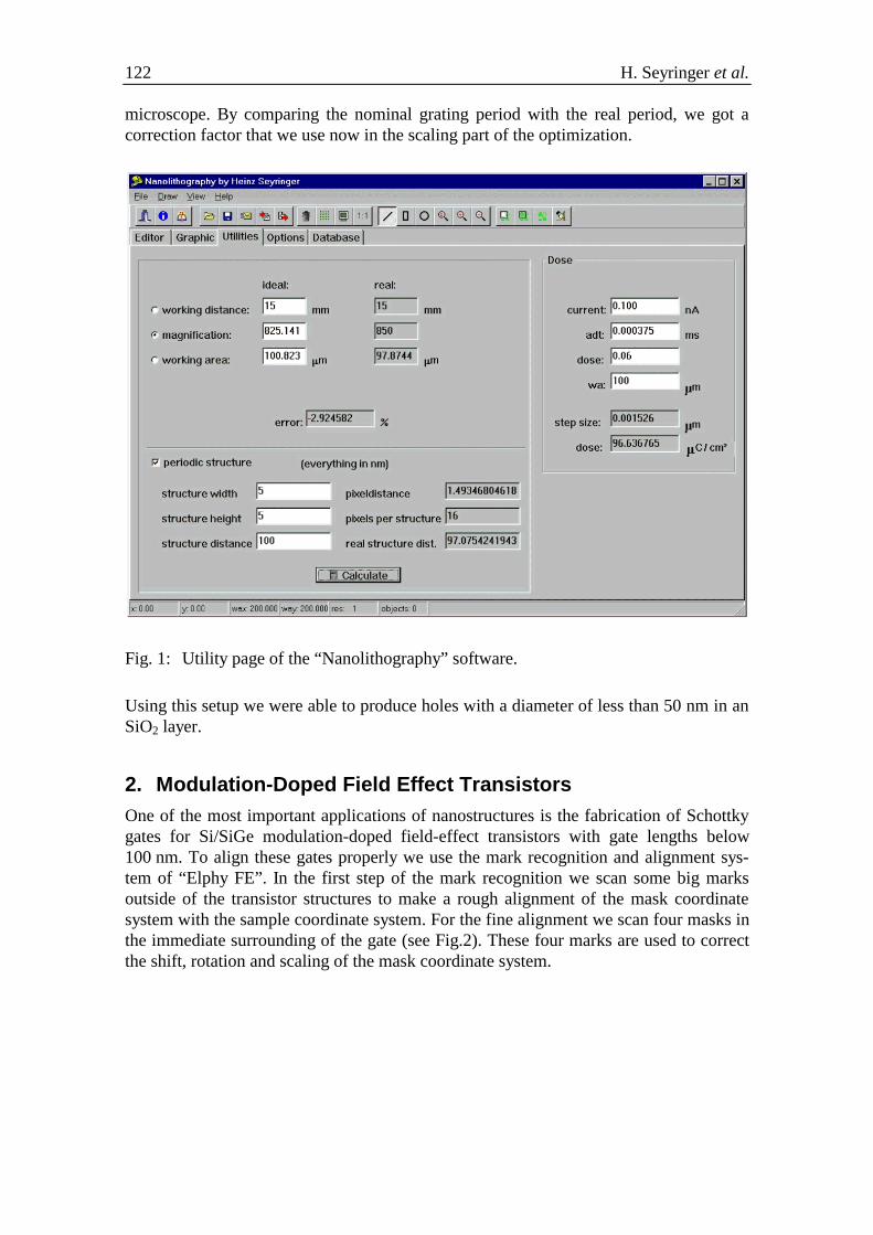
122 H. Seyringer et al.
microscope. By comparing the nominal grating period with the real period, we got acorrection factor that we use now in the scaling part of the optimization.
Fig. 1: Utility page of the “Nanolithography” software.
Using this setup we were able to produce holes with a diameter of less than 50 nm in anSiO2 layer.
2. Modulation-Doped Field Effect TransistorsOne of the most important applications of nanostructures is the fabrication of Schottkygates for Si/SiGe modulation-doped field-effect transistors with gate lengths below100 nm. To align these gates properly we use the mark recognition and alignment sys-tem of “Elphy FE”. In the first step of the mark recognition we scan some big marksoutside of the transistor structures to make a rough alignment of the mask coordinatesystem with the sample coordinate system. For the fine alignment we scan four masks inthe immediate surrounding of the gate (see Fig.2). These four marks are used to correctthe shift, rotation and scaling of the mask coordinate system.
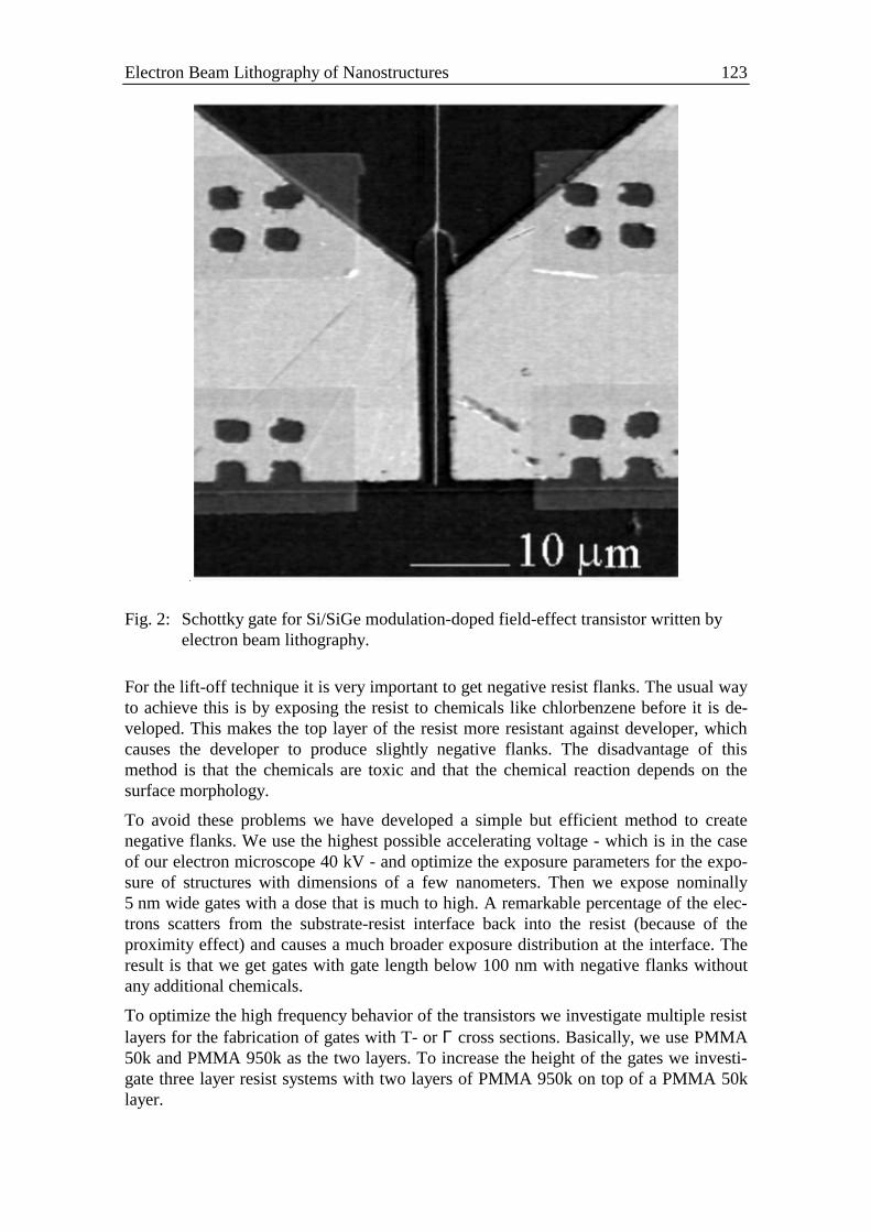
Electron Beam Lithography of Nanostructures 123
Fig. 2: Schottky gate for Si/SiGe modulation-doped field-effect transistor written byelectron beam lithography.
For the lift-off technique it is very important to get negative resist flanks. The usual wayto achieve this is by exposing the resist to chemicals like chlorbenzene before it is de-veloped. This makes the top layer of the resist more resistant against developer, whichcauses the developer to produce slightly negative flanks. The disadvantage of thismethod is that the chemicals are toxic and that the chemical reaction depends on thesurface morphology.
To avoid these problems we have developed a simple but efficient method to createnegative flanks. We use the highest possible accelerating voltage - which is in the caseof our electron microscope 40 kV - and optimize the exposure parameters for the expo-sure of structures with dimensions of a few nanometers. Then we expose nominally5 nm wide gates with a dose that is much to high. A remarkable percentage of the elec-trons scatters from the substrate-resist interface back into the resist (because of theproximity effect) and causes a much broader exposure distribution at the interface. Theresult is that we get gates with gate length below 100 nm with negative flanks withoutany additional chemicals.
To optimize the high frequency behavior of the transistors we investigate multiple resistlayers for the fabrication of gates with T- or Γ cross sections. Basically, we use PMMA50k and PMMA 950k as the two layers. To increase the height of the gates we investi-gate three layer resist systems with two layers of PMMA 950k on top of a PMMA 50klayer.
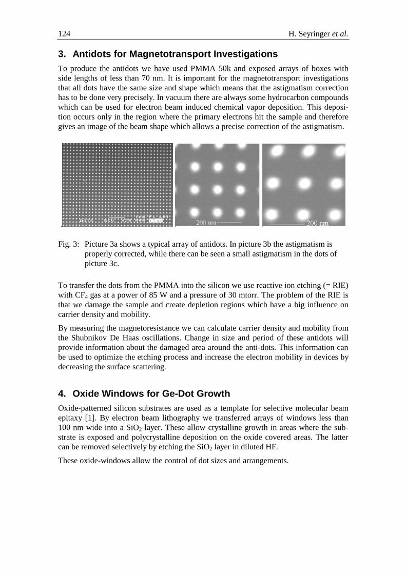
124 H. Seyringer et al.
3. Antidots for Magnetotransport InvestigationsTo produce the antidots we have used PMMA 50k and exposed arrays of boxes withside lengths of less than 70 nm. It is important for the magnetotransport investigationsthat all dots have the same size and shape which means that the astigmatism correctionhas to be done very precisely. In vacuum there are always some hydrocarbon compoundswhich can be used for electron beam induced chemical vapor deposition. This deposi-tion occurs only in the region where the primary electrons hit the sample and thereforegives an image of the beam shape which allows a precise correction of the astigmatism.
Fig. 3: Picture 3a shows a typical array of antidots. In picture 3b the astigmatism isproperly corrected, while there can be seen a small astigmatism in the dots ofpicture 3c.
To transfer the dots from the PMMA into the silicon we use reactive ion etching (= RIE)with CF4 gas at a power of 85 W and a pressure of 30 mtorr. The problem of the RIE isthat we damage the sample and create depletion regions which have a big influence oncarrier density and mobility.
By measuring the magnetoresistance we can calculate carrier density and mobility fromthe Shubnikov De Haas oscillations. Change in size and period of these antidots willprovide information about the damaged area around the anti-dots. This information canbe used to optimize the etching process and increase the electron mobility in devices bydecreasing the surface scattering.
4. Oxide Windows for Ge-Dot GrowthOxide-patterned silicon substrates are used as a template for selective molecular beamepitaxy [1]. By electron beam lithography we transferred arrays of windows less than100 nm wide into a SiO2 layer. These allow crystalline growth in areas where the sub-strate is exposed and polycrystalline deposition on the oxide covered areas. The lattercan be removed selectively by etching the SiO2 layer in diluted HF.
These oxide-windows allow the control of dot sizes and arrangements.
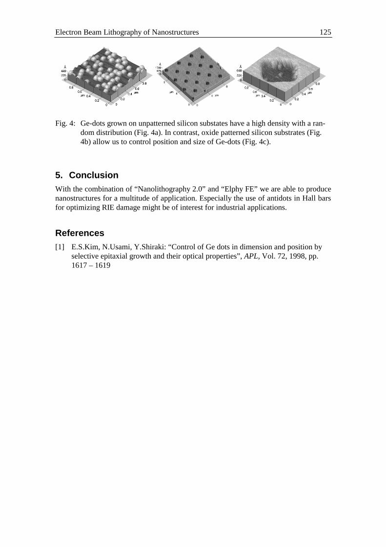
Electron Beam Lithography of Nanostructures 125
Fig. 4: Ge-dots grown on unpatterned silicon substates have a high density with a ran-dom distribution (Fig. 4a). In contrast, oxide patterned silicon substrates (Fig.4b) allow us to control position and size of Ge-dots (Fig. 4c).
5. ConclusionWith the combination of “Nanolithography 2.0” and “Elphy FE” we are able to producenanostructures for a multitude of application. Especially the use of antidots in Hall barsfor optimizing RIE damage might be of interest for industrial applications.
References[1] E.S.Kim, N.Usami, Y.Shiraki: “Control of Ge dots in dimension and position by
selective epitaxial growth and their optical properties”, APL, Vol. 72, 1998, pp.1617 – 1619

The Society for Microelectronics – Annual Report 1999 127
Fabrication of SemiconductorNanostructures by Scanning Force
MicroscopyK. Wiesauer and G. Springholz
Institut für Halbleiter- und Festkörperphysik,Johannes Kepler Universität Linz, A-4040 Linz, Austria
A process for fabrication of semiconductor nanostructures using scanning force mi-croscopy (AFM) in combination with conventional optical lithography is described.It is based on the mechanical modification of ultra-thin photoresist layers with super-sharp AFM tips and subsequent pattern transfer by reactive ion etching. Minimalfeature sizes of 45 nm and periods of 88 nm were achieved by this technique.
1. IntroductionThe fabrication of semiconductor nanostructures for the development of quantum elec-tronic devices has attracted tremendous interest in the last few years. In such devices,the electron wavelengths of typically 20 – 50 nm are comparable to the device dimen-sions. Therefore, the electronic properties are dominated by quantum phenomena. Therealization of nanostructures remains a big technological challenge. Although withscanning probe microscopy controlled surface modifications have become possibledown to the level of single adatoms [1], for practical applications one would like tocombine the high lateral resolution of scanning probe techniques with existing semicon-ductor process technologies [2]. In the present work, we have developed a process se-quence that combines conventional optical lithography with mechanical modificationsof ultra-thin photoresist layers with super-sharp atomic force microscopy (AFM) tips[3]. This allows an efficient definition of very large, as well as nanoscale resist patternswith subsequent pattern transfer to the substrate in one single reactive ion etching step.
2. Process DescriptionThe AFM patterning is realized by indentation of an AFM tip into a soft photoresistlayer. This produces well defined structures where the resist is locally removed. Theminimal feature size is mainly determined by three parameters, namely, 1) the resistthickness, 2) the size and shape of the AFM tips, and 3) the directionality of the finalpattern transfer process. For optimum results the use of ultra-thin photoresist layers is ofparticular importance because the size of bulge of the displaced photoresist around theholes is the main limitation for the minimal feature separation.
2.1 Lithography with Ultra-Thin Photoresists
To produce an ultra-thin photoresist layer, the positive resist ‘Shipley S1805’ is dilutedwith a thinner (’Shipley EC Solvent’) in the proportion 1:12 to 1:15. The highly thinnedphotoresist is spin-coated on the sample with 5500 rpm, forming a homogeneous layer
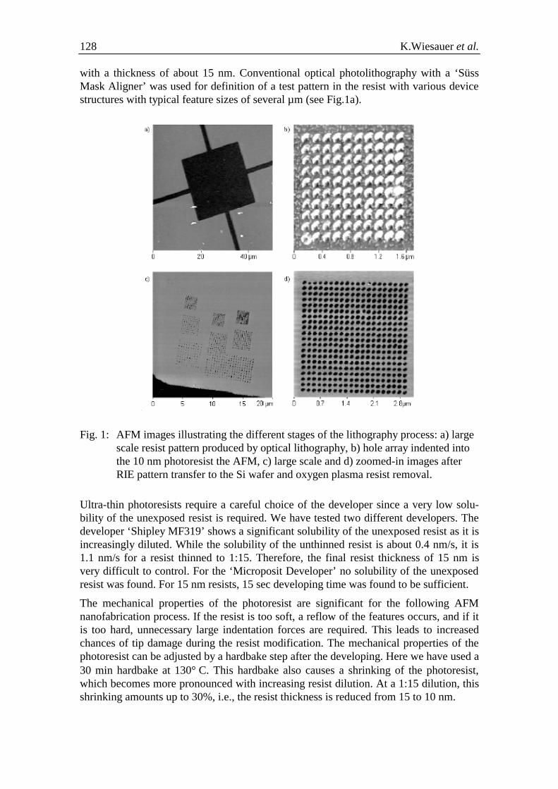
128 K.Wiesauer et al.
with a thickness of about 15 nm. Conventional optical photolithography with a ‘SüssMask Aligner’ was used for definition of a test pattern in the resist with various devicestructures with typical feature sizes of several µm (see Fig.1a).
Fig. 1: AFM images illustrating the different stages of the lithography process: a) largescale resist pattern produced by optical lithography, b) hole array indented intothe 10 nm photoresist the AFM, c) large scale and d) zoomed-in images afterRIE pattern transfer to the Si wafer and oxygen plasma resist removal.
Ultra-thin photoresists require a careful choice of the developer since a very low solu-bility of the unexposed resist is required. We have tested two different developers. Thedeveloper ‘Shipley MF319’ shows a significant solubility of the unexposed resist as it isincreasingly diluted. While the solubility of the unthinned resist is about 0.4 nm/s, it is1.1 nm/s for a resist thinned to 1:15. Therefore, the final resist thickness of 15 nm isvery difficult to control. For the ‘Microposit Developer’ no solubility of the unexposedresist was found. For 15 nm resists, 15 sec developing time was found to be sufficient.
The mechanical properties of the photoresist are significant for the following AFMnanofabrication process. If the resist is too soft, a reflow of the features occurs, and if itis too hard, unnecessary large indentation forces are required. This leads to increasedchances of tip damage during the resist modification. The mechanical properties of thephotoresist can be adjusted by a hardbake step after the developing. Here we have used a30 min hardbake at 130° C. This hardbake also causes a shrinking of the photoresist,which becomes more pronounced with increasing resist dilution. At a 1:15 dilution, thisshrinking amounts up to 30%, i.e., the resist thickness is reduced from 15 to 10 nm.
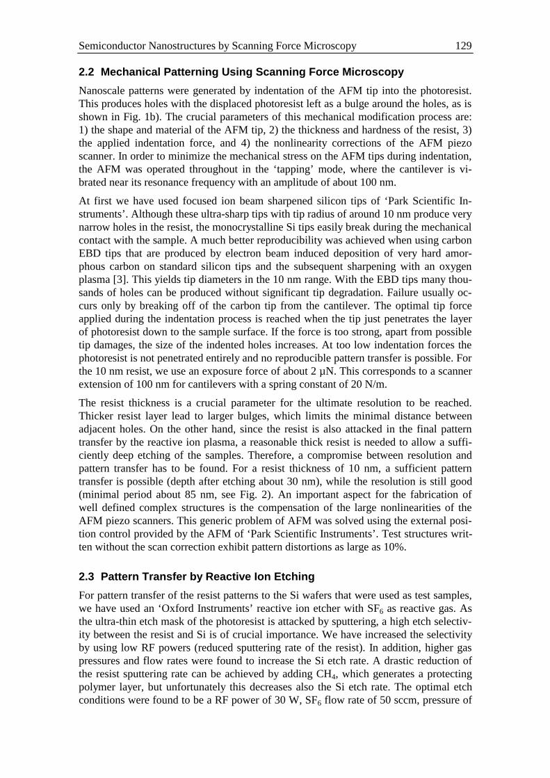
Semiconductor Nanostructures by Scanning Force Microscopy 129
2.2 Mechanical Patterning Using Scanning Force Microscopy
Nanoscale patterns were generated by indentation of the AFM tip into the photoresist.This produces holes with the displaced photoresist left as a bulge around the holes, as isshown in Fig. 1b). The crucial parameters of this mechanical modification process are:1) the shape and material of the AFM tip, 2) the thickness and hardness of the resist, 3)the applied indentation force, and 4) the nonlinearity corrections of the AFM piezoscanner. In order to minimize the mechanical stress on the AFM tips during indentation,the AFM was operated throughout in the ‘tapping’ mode, where the cantilever is vi-brated near its resonance frequency with an amplitude of about 100 nm.
At first we have used focused ion beam sharpened silicon tips of ‘Park Scientific In-struments’. Although these ultra-sharp tips with tip radius of around 10 nm produce verynarrow holes in the resist, the monocrystalline Si tips easily break during the mechanicalcontact with the sample. A much better reproducibility was achieved when using carbonEBD tips that are produced by electron beam induced deposition of very hard amor-phous carbon on standard silicon tips and the subsequent sharpening with an oxygenplasma [3]. This yields tip diameters in the 10 nm range. With the EBD tips many thou-sands of holes can be produced without significant tip degradation. Failure usually oc-curs only by breaking off of the carbon tip from the cantilever. The optimal tip forceapplied during the indentation process is reached when the tip just penetrates the layerof photoresist down to the sample surface. If the force is too strong, apart from possibletip damages, the size of the indented holes increases. At too low indentation forces thephotoresist is not penetrated entirely and no reproducible pattern transfer is possible. Forthe 10 nm resist, we use an exposure force of about 2 µN. This corresponds to a scannerextension of 100 nm for cantilevers with a spring constant of 20 N/m.
The resist thickness is a crucial parameter for the ultimate resolution to be reached.Thicker resist layer lead to larger bulges, which limits the minimal distance betweenadjacent holes. On the other hand, since the resist is also attacked in the final patterntransfer by the reactive ion plasma, a reasonable thick resist is needed to allow a suffi-ciently deep etching of the samples. Therefore, a compromise between resolution andpattern transfer has to be found. For a resist thickness of 10 nm, a sufficient patterntransfer is possible (depth after etching about 30 nm), while the resolution is still good(minimal period about 85 nm, see Fig. 2). An important aspect for the fabrication ofwell defined complex structures is the compensation of the large nonlinearities of theAFM piezo scanners. This generic problem of AFM was solved using the external posi-tion control provided by the AFM of ‘Park Scientific Instruments’. Test structures writ-ten without the scan correction exhibit pattern distortions as large as 10%.
2.3 Pattern Transfer by Reactive Ion Etching
For pattern transfer of the resist patterns to the Si wafers that were used as test samples,we have used an ‘Oxford Instruments’ reactive ion etcher with SF6 as reactive gas. Asthe ultra-thin etch mask of the photoresist is attacked by sputtering, a high etch selectiv-ity between the resist and Si is of crucial importance. We have increased the selectivityby using low RF powers (reduced sputtering rate of the resist). In addition, higher gaspressures and flow rates were found to increase the Si etch rate. A drastic reduction ofthe resist sputtering rate can be achieved by adding CH4, which generates a protectingpolymer layer, but unfortunately this decreases also the Si etch rate. The optimal etchconditions were found to be a RF power of 30 W, SF6 flow rate of 50 sccm, pressure of
130 K.Wiesauer et al.
40 mtorr and a CH4 flow of 25 sccm. This results in an etch rate for Si of 49 nm/min andof 6 nm/min for the resist. Finally, the photoresist is stripped from the sample in thesame RIE reactor with an oxygen plasma (90W, 10 sccm, 60 mtorr). The resulting pat-terns after these processing steps are shown in Fig. 1 c) and d).
Fig. 2: Atomic force microscopy image and cross sectional profile of a periodic holearray in Si fabricated by AFM nanolithography. Array with 10 x 10 holes with aperiod of 88 nm, hole diameter of 44 nm and hole depth of 16 nm.
3. Summary of the ResultsThe minimal feature sizes that were made by the combined optical and AFM lithogra-phy process are shown in Fig. 2. The test pattern of a periodic hole array exhibits featurediameters of about 44 nm with an etch depth of about 30 nm. Minimal grating periods of88 nm were achieved. Apart from such hole structures we have also fabricated lines with45 nm line widths. The lines were drawn by putting a series of holes in very closeproximity (less than 30 nm) to each other. In this way also more complicated structurescan be made. The largest dot arrays we have produced so far consisted of several thou-sand individual dots and exhibited no apparent pattern distortions within fields of sev-eral micrometer in size. The big advantage of our approach is that is a mask-based li-thography technique that is independent of the substrate and which allows the use ofproven semiconductor processing steps. Therefore, we were able use our method forGaAs nanostructure fabrication just by modifying the final etching process.
References[1] D. M. Eigler and E. K. Schweizer, “Positioning Single Atoms with a Scanning
Tunneling Microscope”, Nature, Vol. 344, 1990, p. 524.
[2] E. S. Snow, P. M. Campbell, and F. K. Perkins, “Nanofabrication with ProximalProbes”, Proc. IEEE, Vol. 85, 1997, p. 601.
[3] M. Wendel, H. Lorenz, and J. P. Kotthaus, “Sharpened Electron Beam DepositedTips for High Resolution Atomic Force Microscope Lithography and Imaging”,Appl. Phys. Lett., Vol. 67, 1995, p. 3732.
The Society for Microelectronics – Annual Report 1999 131
Light Generation by Er in Si RelatedMaterials
S. Lanzerstorfer, M. Stepikhova, H. Preier, L. Palmetshofer, W. Jantsch
Institut für Halbleiter- und Festkörperphysik, Johannes Kepler UniversitätLinz, Altenbergerstr. 69, A-4040 Linz
Er-doped Si is utilized for Si-based light generation in the 1.54 µm region, which isof particular interest for optical data communication. The main problem of Si: Erwas so far the huge temperature quenching of the luminescence yield of forward bi-ased diodes. It turned out that properly designed diodes driven in reverse bias avoidthis temperature quenching due to different excitation and deexcitation mechanisms.The fabrication and annealing conditions for maximum luminescence yield at roomtemperature are presented.
1. IntroductionOne of the last unsolved problems and challenges in Si technology is the integration ofcompatible light sources as needed for optical communication within or between chips.Although there are different approaches followed worldwide, there is no obvious solu-tion so far [1]. One of the most promising principles proposed is the light generation byintra-4f transitions in Er, which can be integrated in very different hosts giving alwaysthe same characteristic sharp spectra. Additionally, as a consequence of the wellshielded 4f-shell, the emission wavelength at 1.54 µm is temperature independent. Sincethe first diodes fabricated by Ennen [2] et. al, the temperature quenching of the lumines-cence yield in forward bias is still the main problem, although several groups [3], [4]were focused on Si:Er. The intensity of the room temperature emission in forward bias,however, is rather weak and comparable to the dislocation related luminescence.
For reverse bias, a completely different situation occurs. Almost no temperaturequenching of the electroluminescence (EL) signal is observed indicating different exci-tation and deexcitation mechanisms of the Er-ions compared to forward biased diodes[5]. High resolution spectra show, that no additional emission centers are excited in re-verse bias. The excitation efficiency of some specific center is very different in the twoexcitation modes. The efficiency for exciting isolated Er centers with a sharp emission ishigher in forward bias, whereas in reverse bias mainly centers are excited with an emis-sion similar to Er-doped silica. At elevated temperatures only the SiO2 centers are ex-cited, in both forward and reverse biased diodes. Therefore we investigated the prepara-tion conditions for optimum formation of Er-doped SiO2 centers within the Si host,which lie in a narrow region of Er and O concentrations and specific annealing treat-ments after ion implantation.
2. Experimental
Erbium was implanted in n-type (100)-CZ-Si with a resistivity of 10 Ωcm at room tem-perature. The Er-dose at an implantation energy of 300 keV was varied between 1012
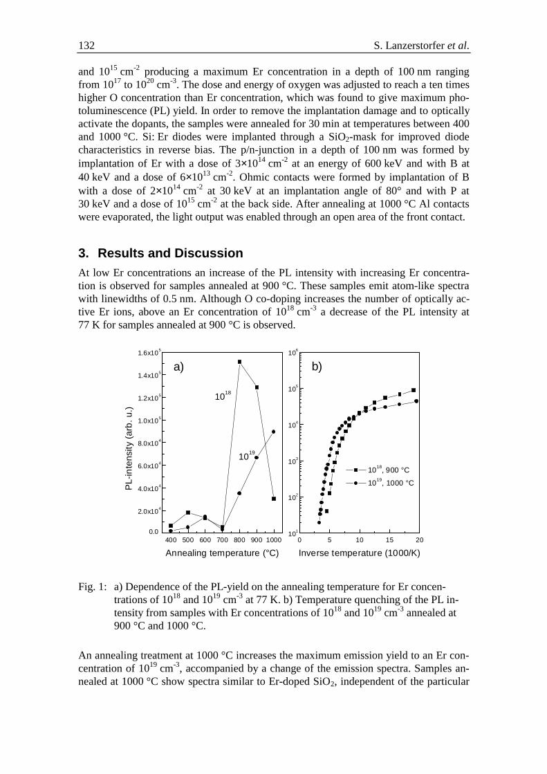
132 S. Lanzerstorfer et al.
and 1015 cm-2 producing a maximum Er concentration in a depth of 100 nm rangingfrom 1017 to 1020 cm-3. The dose and energy of oxygen was adjusted to reach a ten timeshigher O concentration than Er concentration, which was found to give maximum pho-toluminescence (PL) yield. In order to remove the implantation damage and to opticallyactivate the dopants, the samples were annealed for 30 min at temperatures between 400and 1000 °C. Si: Er diodes were implanted through a SiO2-mask for improved diodecharacteristics in reverse bias. The p/n-junction in a depth of 100 nm was formed byimplantation of Er with a dose of 3×1014 cm-2 at an energy of 600 keV and with B at40 keV and a dose of 6×1013 cm-2. Ohmic contacts were formed by implantation of Bwith a dose of 2×1014 cm-2 at 30 keV at an implantation angle of 80° and with P at30 keV and a dose of 1015 cm-2 at the back side. After annealing at 1000 °C Al contactswere evaporated, the light output was enabled through an open area of the front contact.
3. Results and DiscussionAt low Er concentrations an increase of the PL intensity with increasing Er concentra-tion is observed for samples annealed at 900 °C. These samples emit atom-like spectrawith linewidths of 0.5 nm. Although O co-doping increases the number of optically ac-tive Er ions, above an Er concentration of 1018 cm-3 a decrease of the PL intensity at77 K for samples annealed at 900 °C is observed.
400 500 600 700 800 900 10000.0
2.0x10⁴
4.0x10⁴
6.0x10⁴
8.0x10⁴
1.0x10⁵
1.2x10⁵
1.4x10⁵
1.6x10⁵
1019
1018
a)
PL-
inte
nsity
(ar
b. u
.)
Annealing temperature (°C)
0 5 10 15 2010
1
102
103
104
105
106
1018, 900 °C
1019, 1000 °C
b)
Inverse temperature (1000/K)
Fig. 1: a) Dependence of the PL-yield on the annealing temperature for Er concen-trations of 1018 and 1019 cm-3 at 77 K. b) Temperature quenching of the PL in-tensity from samples with Er concentrations of 1018 and 1019 cm-3 annealed at900 °C and 1000 °C.
An annealing treatment at 1000 °C increases the maximum emission yield to an Er con-centration of 1019 cm-3, accompanied by a change of the emission spectra. Samples an-nealed at 1000 °C show spectra similar to Er-doped SiO2, independent of the particular
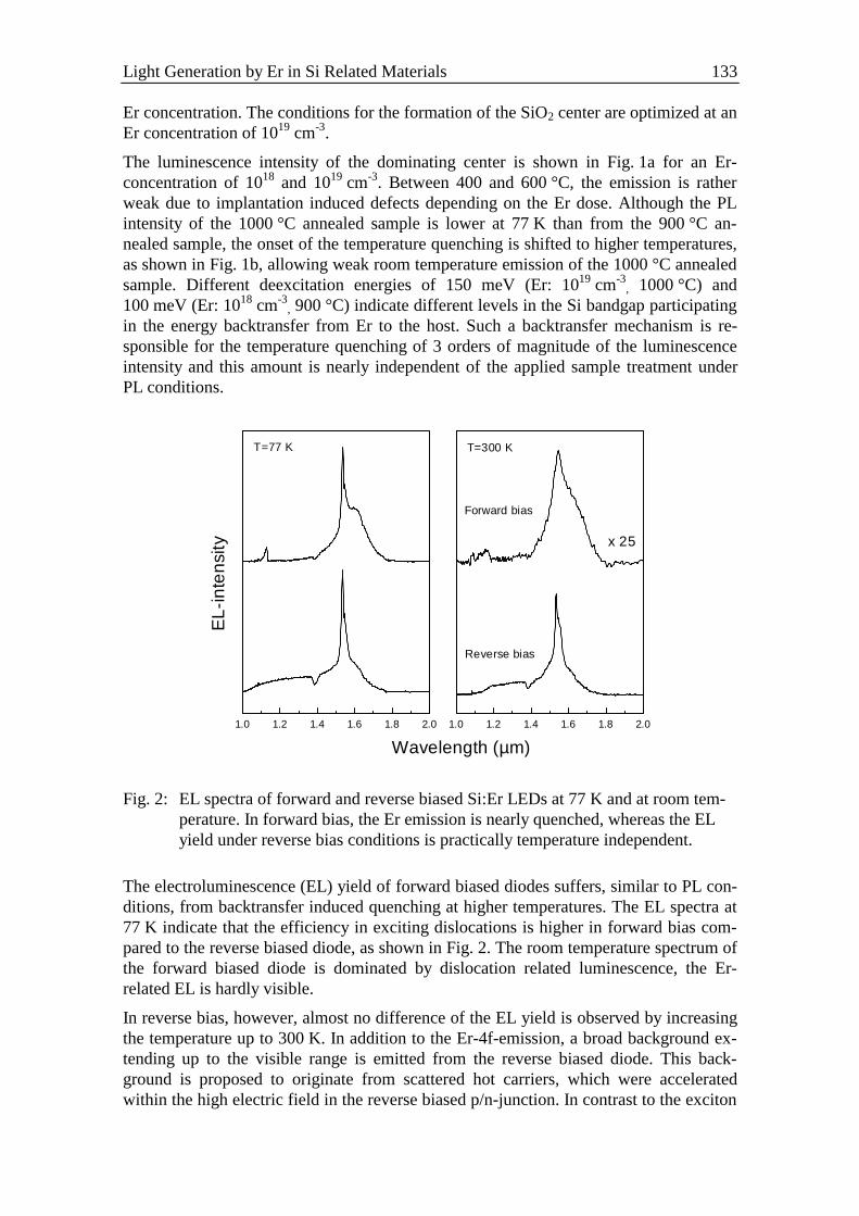
Light Generation by Er in Si Related Materials 133
Er concentration. The conditions for the formation of the SiO2 center are optimized at anEr concentration of 1019 cm-3.
The luminescence intensity of the dominating center is shown in Fig. 1a for an Er-concentration of 1018 and 1019 cm-3. Between 400 and 600 °C, the emission is ratherweak due to implantation induced defects depending on the Er dose. Although the PLintensity of the 1000 °C annealed sample is lower at 77 K than from the 900 °C an-nealed sample, the onset of the temperature quenching is shifted to higher temperatures,as shown in Fig. 1b, allowing weak room temperature emission of the 1000 °C annealedsample. Different deexcitation energies of 150 meV (Er: 1019 cm-3
, 1000 °C) and100 meV (Er: 1018 cm-3
, 900 °C) indicate different levels in the Si bandgap participatingin the energy backtransfer from Er to the host. Such a backtransfer mechanism is re-sponsible for the temperature quenching of 3 orders of magnitude of the luminescenceintensity and this amount is nearly independent of the applied sample treatment underPL conditions.
1.0 1.2 1.4 1.6 1.8 2.0
T=77 K
Reverse bias
Forward bias
x 25
T=300 K
EL
-in
ten
sity
Wavelength (µm)
1.0 1.2 1.4 1.6 1.8 2.0
Fig. 2: EL spectra of forward and reverse biased Si:Er LEDs at 77 K and at room tem-perature. In forward bias, the Er emission is nearly quenched, whereas the ELyield under reverse bias conditions is practically temperature independent.
The electroluminescence (EL) yield of forward biased diodes suffers, similar to PL con-ditions, from backtransfer induced quenching at higher temperatures. The EL spectra at77 K indicate that the efficiency in exciting dislocations is higher in forward bias com-pared to the reverse biased diode, as shown in Fig. 2. The room temperature spectrum ofthe forward biased diode is dominated by dislocation related luminescence, the Er-related EL is hardly visible.
In reverse bias, however, almost no difference of the EL yield is observed by increasingthe temperature up to 300 K. In addition to the Er-4f-emission, a broad background ex-tending up to the visible range is emitted from the reverse biased diode. This back-ground is proposed to originate from scattered hot carriers, which were acceleratedwithin the high electric field in the reverse biased p/n-junction. In contrast to the exciton
134 S. Lanzerstorfer et al.
mediated excitation of forward biased diodes, the Er-ions are impact-excited by hot car-riers under reverse bias [6]. The absence of the strong temperature quenching of the ELyield in reverse bias indicates a different deexcitation as compared to forward bias. Ei-ther the backtransfer path is passivated in the high electric field or only those Er ions areimpact-excited which lie within silica precipitates without efficient energy transfer backto the Si host. The spectra of highly O codoped diodes are similar to Er doped silica,indicating the possibility of Er doped SiO2 precipitates responsible for room temperatureemission.
4. ConclusionThe standard annealing treatment at 900 °C after Er implantation induces the formationof isolated Er centers giving rise for sharp emission at low temperatures. The emissionof those centers, however, is quenched already at temperatures below 200 K. Increasingthe annealing temperature to 1000 °C removes all sharp lines, the obtained spectra aresimilar to those of Er doped silica. The EL spectra of Si: Er diodes indicate that mainlythose Er doped silica precipitates are excited in reverse bias. Therefore, the conditionsfor the formation of this particular center were optimized. Strong room temperature ELwas obtained from diodes in reverse bias with an Er concentration of 1019 cm-3 and anannealing treatment at 1000 °C.
AcknowledgementsPart of the work was supported by the Gesellschaft für Mikroelektronik and the Fondszur Förderung der Wissenschaftlichen Forschung, Wien.
References[1] R. A. Soref: “Silicon-based optoelectronics”, Proc. IEEE, Vol. 81, 1993, pp.
1687 – 1706.
[2] H. Ennen, G. Pomrenke, A. Axmann, K. Eisele, W. Haydl, and J. Schneider:“1.54 µm electroluminescence of erbium-doped silicon grown by molecular beamepitaxy”, Appl. Phys. Lett., Vol. 46, 1985, pp. 381 – 383.
[3] A. Polman, G. N. van den Hoven, J. S. Custer, J. H. Shin, R. Serna, and P. F. A.Alkemade: “Erbium in crystal silicon: Optical activation, excitation, andconcentration limits”, J. Appl. Phys., Vol. 77, 1995, pp. 1256 – 1262.
[4] F. Priolo, G. Franzo, S. Coffa, A. Carnera: “Excitation and nonradiativedeexcitation processes of Er3+ in crystalline Si”, Phys. Rev. B, Vol. 57, 1998, pp.4443 – 4455.
[5] J. Stimmer, A. Reittinger, J. F. Nützel, G. Abstreiter, H. Holzbrecher, and Ch.Buchal: “Electroluminescence of erbium-oxygen-doped silicon diodes grown bymolecular beam epitaxy”, Appl. Phys. Lett., Vol. 68, 1996, pp. 3290 – 3292.
[6] S. Coffa, G. Franzo, F. Priolo, A. Pacelli, and A. Lacaita: “Direct evidence ofimpact excitation and spatial profiling of excited Er in light emitting Si diodes”,Appl. Phys. Lett., Vol. 73, 1998, pp. 93 – 95.
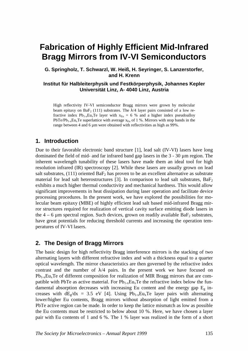
The Society for Microelectronics – Annual Report 1999 135
Fabrication of Highly Efficient Mid-InfraredBragg Mirrors from IV-VI Semiconductors
G. Springholz, T. Schwarzl, W. Heiß, H. Seyringer, S. Lanzerstorfer,and H. Krenn
Institut für Halbleiterphysik und Festkörperphysik, Johannes KeplerUniversität Linz, A- 4040 Linz, Austria
High reflectivity IV-VI semiconductor Bragg mirrors were grown by molecularbeam epitaxy on BaF2 (111) substrates. The λ/4 layer pairs consisted of a low re-fractive index Pb1-xEuxTe layer with xEu = 6 % and a higher index pseudoalloyPbTe/Pb1-xEuxTe superlattice with average xEu of 1 %. Mirrors with stop bands in therange between 4 and 6 µm were obtained with reflectivities as high as 99%.
1. IntroductionDue to their favorable electronic band structure [1], lead salt (IV-VI) lasers have longdominated the field of mid- and far infrared band gap lasers in the 3 - 30 µm region. Theinherent wavelength tunability of these lasers have made them an ideal tool for highresolution infrared (IR) spectroscopy [2]. While these lasers are usually grown on leadsalt substrates, (111) oriented BaF2 has proven to be an excellent alternative as substratematerial for lead salt heterostructures [3]. In comparison to lead salt substrates, BaF2
exhibits a much higher thermal conductivity and mechanical hardness. This would allowsignificant improvements in heat dissipation during laser operation and facilitate deviceprocessing procedures. In the present work, we have explored the possibilities for mo-lecular beam epitaxy (MBE) of highly efficient lead salt based mid-infrared Bragg mir-ror structures required for realization of vertical cavity surface emitting diode lasers inthe 4 – 6 µm spectral region. Such devices, grown on readily available BaF2 substrates,have great potentials for reducing threshold currents and increasing the operation tem-peratures of IV-VI lasers.
2. The Design of Bragg MirrorsThe basic design for high reflectivity Bragg interference mirrors is the stacking of twoalternating layers with different refractive index and with a thickness equal to a quarteroptical wavelength. The mirror characteristics are then governed by the refractive indexcontrast and the number of λ/4 pairs. In the present work we have focused onPb1-xEuxTe of different composition for realization of MIR Bragg mirrors that are com-patible with PbTe as active material. For Pb1-xEuxTe the refractive index below the fun-damental absorption decreases with increasing Eu content and the energy gap Eg in-creases with dEg/dx = 3.5 eV [4]. Using Pb1-xEuxTe layer pairs with alternatinglower/higher Eu contents, Bragg mirrors without absorption of light emitted from aPbTe active region can be made. In order to keep the lattice mismatch as low as possiblethe Eu contents must be restricted to below about 10 %. Here, we have chosen a layerpair with Eu contents of 1 and 6 %. The 1 % layer was realized in the form of a short
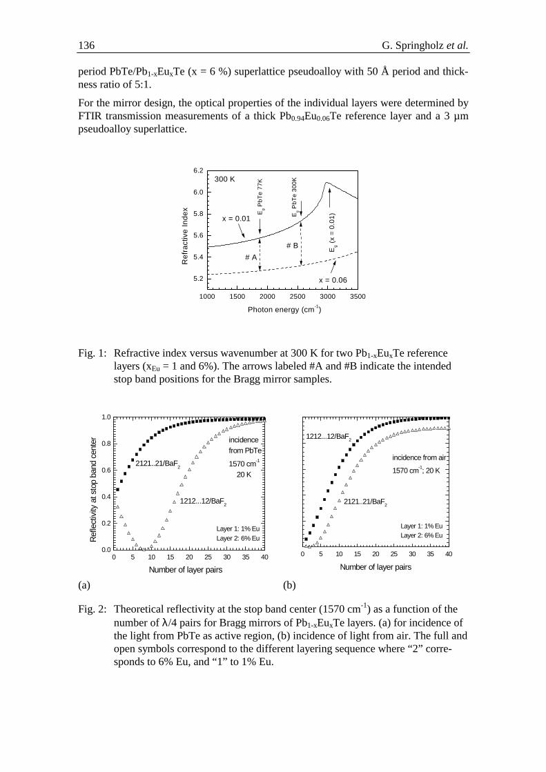
136 G. Springholz et al.
period PbTe/Pb1-xEuxTe (x = 6 %) superlattice pseudoalloy with 50 Å period and thick-ness ratio of 5:1.
For the mirror design, the optical properties of the individual layers were determined byFTIR transmission measurements of a thick Pb0.94Eu0.06Te reference layer and a 3 µmpseudoalloy superlattice.
1000 1500 2000 2500 3000 3500
5.2
5.4
5.6
5.8
6.0
6.2
Eg
Pb
Te
30
0K300 K
Eg
Pb
Te
77
K
# B
# A
Eg
(x =
0.0
1)
x = 0.06
x = 0.01
Re
fra
ctiv
e I
nd
ex
Photon energy (cm-1)
Fig. 1: Refractive index versus wavenumber at 300 K for two Pb1-xEuxTe referencelayers (xEu = 1 and 6%). The arrows labeled #A and #B indicate the intendedstop band positions for the Bragg mirror samples.
0 5 10 15 20 25 30 35 400.0
0.2
0.4
0.6
0.8
1.0
Number of layer pairs
Ref
lect
ivity
at s
top
band
cen
ter
1212...12/BaF2
2121..21/BaF2
Layer 1: 1% EuLayer 2: 6% Eu
incidence from PbTe
1570 cm-1
20 K
0 5 10 15 20 25 30 35 40
1212...12/BaF2
2121..21/BaF2
Layer 1: 1% EuLayer 2: 6% Eu
incidence from air
1570 cm-1; 20 K
Number of layer pairs
(a) (b)
Fig. 2: Theoretical reflectivity at the stop band center (1570 cm-1) as a function of thenumber of λ/4 pairs for Bragg mirrors of Pb1-xEuxTe layers. (a) for incidence ofthe light from PbTe as active region, (b) incidence of light from air. The full andopen symbols correspond to the different layering sequence where “2” corre-sponds to 6% Eu, and “1” to 1% Eu.
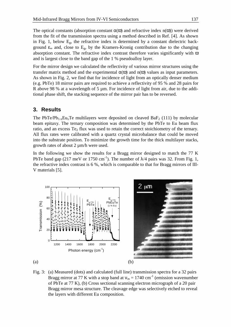
Mid-Infrared Bragg Mirrors from IV-VI Semiconductors 137
The optical constants (absorption constant α(ω) and refractive index n(ω)) were derivedfrom the fit of the transmission spectra using a method described in Ref. [4]. As shownin Fig. 1, below Eg, the refractive index is determined by a constant dielectric back-ground ε∞ and, close to Eg, by the Kramers-Kronig contribution due to the changingabsorption constant. The refractive index contrast therefore varies significantly with ωand is largest close to the band gap of the 1 % pseudoalloy layer.
For the mirror design we calculated the reflectivity of various mirror structures using thetransfer matrix method and the experimental α(ω) and n(ω) values as input parameters.As shown in Fig. 2, we find that for incidence of light from an optically denser medium(e.g. PbTe) 18 mirror pairs are required to achieve a reflectivity of 95 % and 28 pairs forR above 98 % at a wavelength of 5 µm. For incidence of light from air, due to the addi-tional phase shift, the stacking sequence of the mirror pair has to be reversed.
3. ResultsThe PbTe/Pb1-xEuxTe multilayers were deposited on cleaved BaF2 (111) by molecularbeam epitaxy. The ternary composition was determined by the PbTe to Eu beam fluxratio, and an excess Te2 flux was used to retain the correct stoichiometry of the ternary.All flux rates were calibrated with a quartz crystal microbalance that could be movedinto the substrate position. To minimize the growth time for the thick multilayer stacks,growth rates of about 2 µm/h were used.
In the following we show the results for a Bragg mirror designed to match the 77 KPbTe band gap (217 meV or 1750 cm-1). The number of λ/4 pairs was 32. From Fig. 1,the refractive index contrast is 6 %, which is comparable to that for Bragg mirrors of III-V materials [5].
1200 1400 1600 1800 2000 22000
20
40
60
80
100
(1 % Eu)
Eg,77K
PbEuTeEg,77K
PbTe
Tra
nsm
issi
on
(%
)
Photon energy (cm-1
)
(a) (b)
Fig. 3: (a) Measured (dots) and calculated (full line) transmission spectra for a 32 pairsBragg mirror at 77 K with a stop band at νm = 1740 cm-1 (emission wavenumberof PbTe at 77 K), (b) Cross sectional scanning electron micrograph of a 20 pairBragg mirror mesa structure. The cleavage edge was selectively etched to revealthe layers with different Eu composition.
138 G. Springholz et al.
Due to the pseudoalloy superlattices the required total number of individual layers is3230 and the total thickness of the Bragg mirror is 16 µm. The sequence of the λ/4pairs, starting with the 6 % Pb1-xEuxTe on BaF2, was chosen to yield a high reflectivityfor incidence of the light from air. The structural properties of the Bragg mirrors weredetermined by high resolution x-ray diffraction and scanning electron microscopy(SEM). The right hand side of Fig. 3 shows a cross sectional SEM micrograph of a 20pair Bragg mirror sample with mesa structure, demonstrating the high lateral homoge-neity and smooth interface structure of the samples. The cleavage edge was selectivelyetched to reveal the λ/4 layers with different Eu composition using a CH4/H2 plasmaetch. The dark layers correspond to the λ/4 layers with the lower average Eu content, butthe short period superlattice structure of this pseudoalloy layer can be resolved only byx-ray diffraction.
The FTIR transmission spectra of the 32 pair Bragg mirror sample measured at 77 K isshown in Fig. 3 (a). The main features are (1) the Fabry-Perot interference fringes due tothe multiple reflections at the sample surface and the layer/BaF2 interface, (2) the stopband of low transmittance of the Bragg mirror at νm = 1740 cm-1, and (3) the high fre-quency cut off at around 2150 cm-1 due to the absorption edge of the 1 % Pb1-xEuxTepseudo-alloy. The spacing of the fringes corresponds to the inverse optical thickness ofthe multilayer stack. The large refractive index jump at the BaF2 interface also enhancesthe Bragg reflectivity of the samples. The transmission in the stop band region is below0.5 %, which indicates a mirror reflectivity of better than 99 % (negligible absorptionlosses in the stop band region). Bragg mirrors with 20 λ/4 pairs typically exhibit a largerstop band transmission with corresponding reflectivity of about 93 %. Both values agreevery well with our calculations. In spite of the large total thicknesses and large numberof layers we have obtained excellent control and reproducibility of the layer thicknessesand composition. This opens promising perspectives for fabrication and applications ofIV-VI mid-infrared resonant cavity light emitting diodes and vertical cavity surfaceemitting laser devices.
AcknowledgmentsThis work was supported by the OÖ Sparkasse Forschungsförderung, Austria.
References[1] G. Bauer, M. Kriechbaum, Z. Shi, and M. Tacke, “IV-VI Quantum Wells for
infrared lasers”, J. Nonlin. Opt. Phys. Mat., Vol. 4, 1995, pp. 283 – 312.
[2] M. Tacke, Infrared Phys. Technol., Vol. 36, 1995, pp. 447.
[3] A. Y. Ueta, G. Springholz, and G. Bauer, “Improved nucleation and spiral growthof PbTe on BaF2 (111)” J. Cryst. Growth, Vol. 175/176, 1997, pp. 320 – 325.
[4] S. Yuan, H. Krenn, G. Springholz, and G. Bauer, “Dispersion of absorption andrefractive index of PbTe and PbEuTe below and above the fundamental gap” Phys.Rev. B, Vol. 47, 1993, pp. 7213 – 7221.
The Society for Microelectronics – Annual Report 1999 139
CH4/H2 Plasma Etching of IV-VISemiconductors
Th. Schwarzl, W. Heiß, G. Kocher-Oberlehner, and G. Springholz
Institut für Halbleiter- und Festkörperphysik, Johannes Kepler UniversitätLinz, A-4040 Linz, Austria
We demonstrate for the first time CH4/H2 plasma etching of IV-VI nanostructures.Similar as for II-VI compounds, we find a power law dependence between the etchrate and the energy band gap. However, if other than group IV elements are incorpo-rated in the crystal, the etch rate deviates from this behavior. In particular, forPb1-xEuxTe the etch rates drastically decrease with increasing Eu content, which canbe used, e. g., for preferential etching.
1. IntroductionThe narrow gap IV-VI semiconductor compounds have major importance for the fabri-cation of mid infrared optoelectronic devices like lasers and detectors operating in thespectral range between 3 µm and 30 µm [1]. In the fabrication of such devices litho-graphic patterning and etching are of crucial importance. Up to now only wet chemicaletching has been used for the fabrication of buried IV-VI heterostructure lasers. For III-V and II-VI semiconductors, however, it has been shown that plasma etching is superiorin several aspects as compared to wet chemical etching. In this work we demonstrate forthe first time the feasibility of CH4/H2 plasma etching for the structurization of IV-VIsemiconductors.
2. Experimental ProceduresOur etching experiments are performed in a Technics Plasma PP300/M barrel reactoroperating at 2.45 GHz. The samples are placed in the center of the reactor, which con-sists of a glass chamber with a total length of 40 cm and a diameter of 24.5 cm. The gasflow through the reactor is controlled by mass flow controllers for CH4, H2, and Ar, andthe pressure is adjusted at about 0.3 mbar by a control valve to the vacuum pump. Thetypical steady state temperature of the samples during plasma etching reaches 150 °C.Prior to the etching, photoresist patterns are produced by standard photo lithography.Etch masks are obtained by depositing 500 Å to 1500 Å Cr on the photoresist and sub-sequent lift-off. For our etch experiments we use several micrometer thick molecularbeam epitaxial PbTe, PbSe, and Pb1-xEuxTe layers grown on [111] oriented BaF2 sub-strates. The etch process was characterized by a profilometer and by examining theetched profiles by scanning electron microscopy.
3. Plasma Etching of Different IV-VI CompoundsIn a first set of experiments we etched several different IV-VI semiconductor com-pounds simultaneously in the barrel reactor. Thus, the process parameters (gas flows of
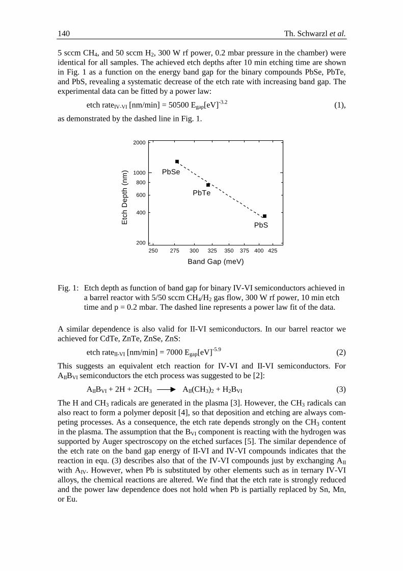
140 Th. Schwarzl et al.
5 sccm CH4, and 50 sccm H2, 300 W rf power, 0.2 mbar pressure in the chamber) wereidentical for all samples. The achieved etch depths after 10 min etching time are shownin Fig. 1 as a function on the energy band gap for the binary compounds PbSe, PbTe,and PbS, revealing a systematic decrease of the etch rate with increasing band gap. Theexperimental data can be fitted by a power law:
etch rateIV-VI [nm/min] = 50500 Egap[eV]-3.2 (1),
as demonstrated by the dashed line in Fig. 1.
250 275 300 325 350 375 400 425200
400
600
800
1000
2000
PbS
PbTe
PbSe
Etc
h D
epth
(nm
)
Band Gap (meV)
Fig. 1: Etch depth as function of band gap for binary IV-VI semiconductors achieved ina barrel reactor with 5/50 sccm CH4/H2 gas flow, 300 W rf power, 10 min etchtime and p = 0.2 mbar. The dashed line represents a power law fit of the data.
A similar dependence is also valid for II-VI semiconductors. In our barrel reactor weachieved for CdTe, ZnTe, ZnSe, ZnS:
etch rateII-VI [nm/min] = 7000 Egap[eV]-5.9 (2)
This suggests an equivalent etch reaction for IV-VI and II-VI semiconductors. ForAIIBVI semiconductors the etch process was suggested to be [2]:
AIIBVI + 2H + 2CH3 AII(CH3)2 + H2BVI (3)
The H and CH3 radicals are generated in the plasma [3]. However, the CH3 radicals canalso react to form a polymer deposit [4], so that deposition and etching are always com-peting processes. As a consequence, the etch rate depends strongly on the CH3 contentin the plasma. The assumption that the BVI component is reacting with the hydrogen wassupported by Auger spectroscopy on the etched surfaces [5]. The similar dependence ofthe etch rate on the band gap energy of II-VI and IV-VI compounds indicates that thereaction in equ. (3) describes also that of the IV-VI compounds just by exchanging AII
with AIV. However, when Pb is substituted by other elements such as in ternary IV-VIalloys, the chemical reactions are altered. We find that the etch rate is strongly reducedand the power law dependence does not hold when Pb is partially replaced by Sn, Mn,or Eu.
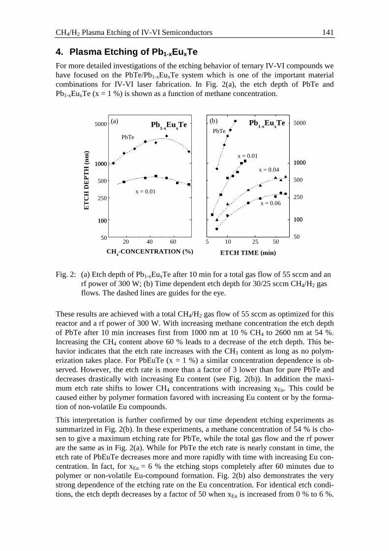
CH4/H2 Plasma Etching of IV-VI Semiconductors 141
4. Plasma Etching of Pb 1-xEuxTeFor more detailed investigations of the etching behavior of ternary IV-VI compounds wehave focused on the PbTe/Pb1-xEuxTe system which is one of the important materialcombinations for IV-VI laser fabrication. In Fig. 2(a), the etch depth of PbTe andPb1-xEuxTe (x = 1 %) is shown as a function of methane concentration.
20 40 6050
100100
250
500
10001000
5000 (a) Pb1-x
EuxTe
x = 0.01
PbTe
ET
CH
DE
PT
H (
nm
)
CH4-CONCENTRATION (%)
5 10 25 5050
100100
250
500
10001000
5000(b) Pb1-x
EuxTe
x = 0.06
x = 0.04
x = 0.01
PbTe
ETCH TIME (min)
Fig. 2: (a) Etch depth of Pb1-xEuxTe after 10 min for a total gas flow of 55 sccm and anrf power of 300 W; (b) Time dependent etch depth for 30/25 sccm CH4/H2 gasflows. The dashed lines are guides for the eye.
These results are achieved with a total CH4/H2 gas flow of 55 sccm as optimized for thisreactor and a rf power of 300 W. With increasing methane concentration the etch depthof PbTe after 10 min increases first from 1000 nm at 10 % CH4 to 2600 nm at 54 %.Increasing the CH4 content above 60 % leads to a decrease of the etch depth. This be-havior indicates that the etch rate increases with the CH3 content as long as no polym-erization takes place. For PbEuTe (x = 1 %) a similar concentration dependence is ob-served. However, the etch rate is more than a factor of 3 lower than for pure PbTe anddecreases drastically with increasing Eu content (see Fig. 2(b)). In addition the maxi-mum etch rate shifts to lower CH4 concentrations with increasing xEu. This could becaused either by polymer formation favored with increasing Eu content or by the forma-tion of non-volatile Eu compounds.
This interpretation is further confirmed by our time dependent etching experiments assummarized in Fig. 2(b). In these experiments, a methane concentration of 54 % is cho-sen to give a maximum etching rate for PbTe, while the total gas flow and the rf powerare the same as in Fig. 2(a). While for PbTe the etch rate is nearly constant in time, theetch rate of PbEuTe decreases more and more rapidly with time with increasing Eu con-centration. In fact, for xEu = 6 % the etching stops completely after 60 minutes due topolymer or non-volatile Eu-compound formation. Fig. 2(b) also demonstrates the verystrong dependence of the etching rate on the Eu concentration. For identical etch condi-tions, the etch depth decreases by a factor of 50 when xEu is increased from 0 % to 6 %.
142 Th. Schwarzl et al.
Therefore, CH4/H2 plasma etching can be used as preferential etch to expose Pb1-xEuxTeheterojunctions.
AcknowledgementsWe would like to thank O. Fuchs and M. Ratajski for technical assistance. This work issupported by the “Fonds zu Förderung der wissenschaftlichen Forschung, FWF,P12100-Phy”, Vienna (Austria).
References[1] A. Katzir, R. Rosman, Y. Shani, K. H. Bachem, H. Böttner, and H. M. Preier,
Handbook of Solid State Lasers, ed. P. K. Cheo, Marcel Dekker Inc. New York,1989, p. 228
[2] A. Semu, L. Montelius, P. Leech, D. Jamieson, P. Silverberg: “Novel CH4/H2
metalorganic reactive ion etching of Hg1-xCdxTe”, Appl. Phys. Lett,. Vol. 59, 1991,pp. 1752 – 1754.
[3] H. Toyoda, H. Kojima, H. Sugai: “Mass spectroscopic investigation of the CH3
radicals in a methane rf discharge”, Appl. Phys. Lett., Vol. 54, 1989, pp. 1507 –1509.
[4] R. Cheung, S. Thoms, S. P. Beamont, G. Doughty, V. Law, C. D. W. Wilkinson:“Reactive ion etching of GaAs using a mixture of methane and hydrogen”Electron. Lett., Vol. 23, 1987, pp. 857 – 858.
[5] M. Neswahl, K. H. Greßlehner, K. Lischka, P. Bauer, A. Brandstötter, K. Lübke:“Properties of dry-etched CdTe-epitaxial layer surfaces and microstructures”,Materials Science and Engineering, Vol. B16, 1993, pp. 108 – 112.
The Society for Microelectronics – Annual Report 1999 143
ZnCdSe/ZnSe Quantum Wires by Epitaxy onPrepatterned GaAs Substrates
W. Heiss, G. Prechtl, D. Stifter, H. Sitter, G. Springholz
Institut für Halbleiter und Festkörperphysik, Universität Linz,Altenbergerstraße 69, A-4040 Linz, Austria
L. Toth
Research Institute for Technical Physics of the Hungarian Academy ofSciences, Ujpest 1, 1325 Budapest, Hungary
The growth rate of ZnSe depends sensitively on the crystalline orientation. This ani-sotropic growth enables us to obtain lateral confinement in quantum wells grown onprepatterned GaAs substrates. We obtain blue light emitting ridge quantum wires anddemonstrate the feasibility to fabricate V-groove quantum wires in II-VI compounds.The lateral confinement is studied by low temperature luminescence experiments.
1. IntroductionZn1-xCdxSe/ZnSe quantum wells can be utilized for the fabrication of laser diodes emit-ting in the blue-green spectral range. For III-V semiconductors it has been demonstratedthat the spike-like density of states in reduced dimensions yields much narrower andhigher gain peak values as compared to quantum well lasers [1]. Up to now, ZnCdSe/ZnSe nanostructures were fabricated by post molecular beam epitaxy (MBE) structuriz-ing and etching techniques [2]. However, these nanostructures suffer from damage in-duced by the etching process, and the optical properties are dominated by nonradiativerecombination and strain relaxation processes [2]. For that reason, we investigate thepossibility to realize quantum wires by MBE on patterned GaAs substrates, to achieve“V-groove” or “ridge” quantum wires.
2. Selectivity of the MBE GrowthAs substrates we prepare (100) oriented GaAs gratings with a period of 800 nm by laserholography and subsequent preferential wet chemical etching. The etching gives trape-zoidal shaped ridges, with (111) and (1-1-1) planes as side walls, embedded betweengrooves with various widths and depths. The substrates were dipped in HCl/H2O beforethey were transferred into the MBE chamber. As reference, an unpatterned GaAs sub-strate was mounted on the same sample holder. The growth was performed at a substratetemperature of 350 °C in an anion enriched growth regime using elementary Zn, Cd, andSe effusion cells. To investigate the anisotropy of the growth, a sample was fabricatedconsisting of a stack of nominally 50 nm thick ZnSe and Zn0.8Cd0.2Se layers. The trans-mission electron micrograph in Fig. 1 shows the cross section of this sample. It clearlydemonstrates that the growth rate of both alloys, the ZnSe and the ZnCdSe, is smaller onthe (111) side walls of the substrate grooves as compared to the (100) oriented substrateregions on the bottom of grooves and on top of the ridges.
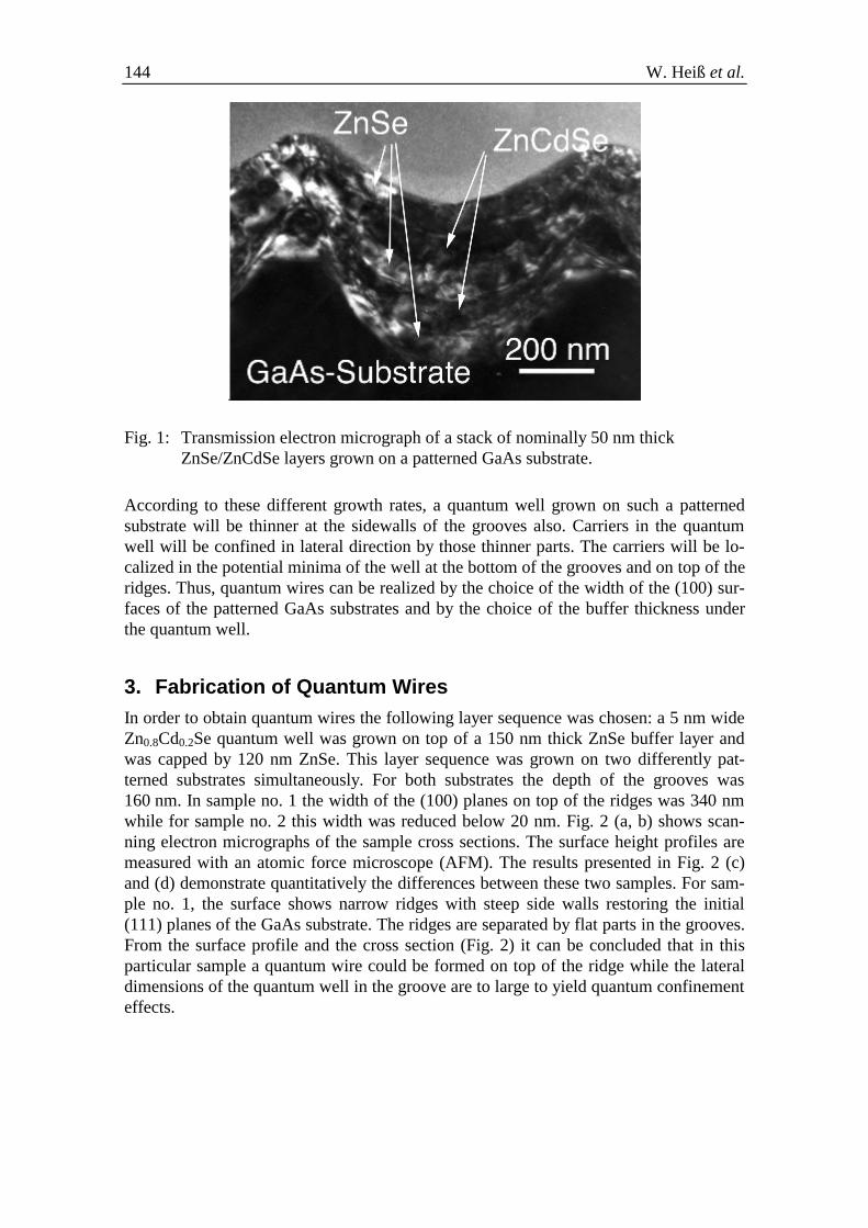
144 W. Heiß et al.
Fig. 1: Transmission electron micrograph of a stack of nominally 50 nm thickZnSe/ZnCdSe layers grown on a patterned GaAs substrate.
According to these different growth rates, a quantum well grown on such a patternedsubstrate will be thinner at the sidewalls of the grooves also. Carriers in the quantumwell will be confined in lateral direction by those thinner parts. The carriers will be lo-calized in the potential minima of the well at the bottom of the grooves and on top of theridges. Thus, quantum wires can be realized by the choice of the width of the (100) sur-faces of the patterned GaAs substrates and by the choice of the buffer thickness underthe quantum well.
3. Fabrication of Quantum WiresIn order to obtain quantum wires the following layer sequence was chosen: a 5 nm wideZn0.8Cd0.2Se quantum well was grown on top of a 150 nm thick ZnSe buffer layer andwas capped by 120 nm ZnSe. This layer sequence was grown on two differently pat-terned substrates simultaneously. For both substrates the depth of the grooves was160 nm. In sample no. 1 the width of the (100) planes on top of the ridges was 340 nmwhile for sample no. 2 this width was reduced below 20 nm. Fig. 2 (a, b) shows scan-ning electron micrographs of the sample cross sections. The surface height profiles aremeasured with an atomic force microscope (AFM). The results presented in Fig. 2 (c)and (d) demonstrate quantitatively the differences between these two samples. For sam-ple no. 1, the surface shows narrow ridges with steep side walls restoring the initial(111) planes of the GaAs substrate. The ridges are separated by flat parts in the grooves.From the surface profile and the cross section (Fig. 2) it can be concluded that in thisparticular sample a quantum wire could be formed on top of the ridge while the lateraldimensions of the quantum well in the groove are to large to yield quantum confinementeffects.
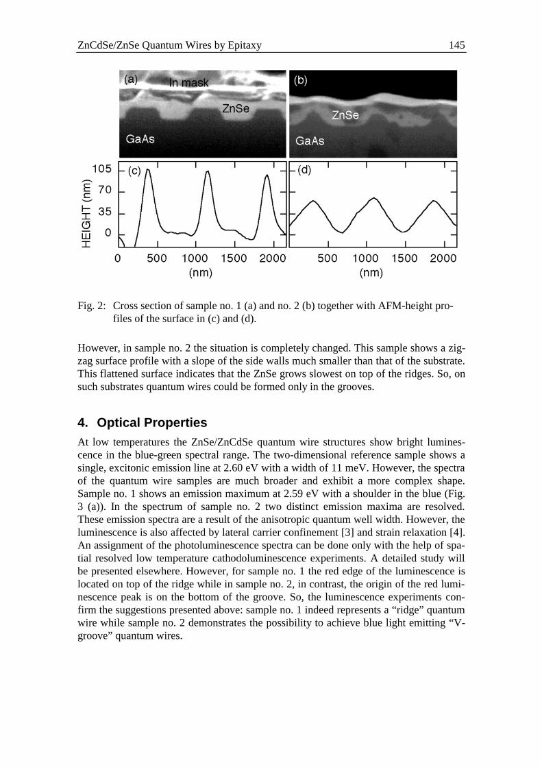
ZnCdSe/ZnSe Quantum Wires by Epitaxy 145
Fig. 2: Cross section of sample no. 1 (a) and no. 2 (b) together with AFM-height pro-files of the surface in (c) and (d).
However, in sample no. 2 the situation is completely changed. This sample shows a zig-zag surface profile with a slope of the side walls much smaller than that of the substrate.This flattened surface indicates that the ZnSe grows slowest on top of the ridges. So, onsuch substrates quantum wires could be formed only in the grooves.
4. Optical PropertiesAt low temperatures the ZnSe/ZnCdSe quantum wire structures show bright lumines-cence in the blue-green spectral range. The two-dimensional reference sample shows asingle, excitonic emission line at 2.60 eV with a width of 11 meV. However, the spectraof the quantum wire samples are much broader and exhibit a more complex shape.Sample no. 1 shows an emission maximum at 2.59 eV with a shoulder in the blue (Fig.3 (a)). In the spectrum of sample no. 2 two distinct emission maxima are resolved.These emission spectra are a result of the anisotropic quantum well width. However, theluminescence is also affected by lateral carrier confinement [3] and strain relaxation [4].An assignment of the photoluminescence spectra can be done only with the help of spa-tial resolved low temperature cathodoluminescence experiments. A detailed study willbe presented elsewhere. However, for sample no. 1 the red edge of the luminescence islocated on top of the ridge while in sample no. 2, in contrast, the origin of the red lumi-nescence peak is on the bottom of the groove. So, the luminescence experiments con-firm the suggestions presented above: sample no. 1 indeed represents a “ridge” quantumwire while sample no. 2 demonstrates the possibility to achieve blue light emitting “V-groove” quantum wires.
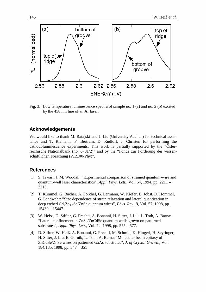
146 W. Heiß et al.
Fig. 3: Low temperature luminescence spectra of sample no. 1 (a) and no. 2 (b) excitedby the 458 nm line of an Ar laser.
AcknowledgementsWe would like to thank M. Ratajski and J. Liu (University Aachen) for technical assis-tance and T. Riemann, F. Bertram, D. Rudloff, J. Christen for performing thecathodoluminescence experiments. This work is partially supported by the “Öster-reichische Nationalbank (no. 6781/2)” and by the “Fonds zur Förderung der wissen-schaftlichen Forschung (P12100-Phy)”.
References[1] S. Tiwari, J. M. Woodall: ”Experimental comparison of strained quantum-wire and
quantum-well laser characteristics”, Appl. Phys. Lett., Vol. 64, 1994, pp. 2211 –2213.
[2] T. Kümmel, G. Bacher, A. Forchel, G. Lermann, W. Kiefer, B. Jobst, D. Hommel,G. Landwehr: ”Size dependence of strain relaxation and lateral quantization indeep etched CdxZn1-xSe/ZnSe quantum wires”, Phys. Rev. B, Vol. 57, 1998, pp.15439 – 15447.
[3] W. Heiss, D. Stifter, G. Prechtl, A. Bonanni, H. Sitter, J. Liu, L. Toth, A. Barna:“Lateral confinement in ZnSe/ZnCdSe quantum wells grown on patternedsubstrates”, Appl. Phys. Lett., Vol. 72, 1998, pp. 575 – 577.
[4] D. Stifter, W. Heiß, A. Bonanni, G. Prechtl, M. Schmid, K. Hingerl, H. Seyringer,H. Sitter, J. Liu, E. Gornik, L. Toth, A. Barna: “Molecular beam epitaxy ofZnCdSe/ZnSe wires on patterned GaAs substrates”, J. of Crystal Growth, Vol.184/185, 1998, pp. 347 – 351
The Society for Microelectronics – Annual Report 1999 147
Self-Assembling Mn-Based NanostructuresA. Bonanni, H. Seyringer, K. Hingerl, and H. Sitter
Institut für Halbleiterphysik, Johannes Kepler Universität, A-4040 Linz
D. Stifter
Profactor GmbH, Wehrgrabengasse 5, A-4040 Steyr
We report on the fabrication, by means of molecular beam epitaxy, of Mn-based na-nostructures on CdTe and on the possibility to obtain regular islands with differentmorphology during the subsequent deposition of semiconductor compounds. Theprocesses are monitored in situ and in real time via reflectance difference spectros-copy.
1. IntroductionIn the area of semiconductor materials, self-assembling nanostructures [1] are attractingconsiderable attention because of their potential applications in electronic and optoelec-tronic devices as e.g. single electron transistors and quantum dot lasers. CdTe-basedsemiconducting magnetic heterostructures (MH), both in the diluted semimagnetic(DMS) phase of Cd1-xMnxTe [2] and in the digital (DMH) arrangement embeddingMnTe magnetic layers [3], [4], offer the unique opportunity of having electronic bandstructures which can considerably be tuned by the application of magnetic fields ofmoderate intensity [5], [6]. In addition, the introduction of magnetic clusters in a semi-conducting matrix opens new perspectives for applications in spin-dependent switchingdevices and in storage technology [7]. Puzzling morphologies of self-assembled islands,depending on the growth conditions and due to strain and stress effects [8], [9] and sur-face diffusion processes, could represent, when properly controlled, interesting newsystems for electronic confinement in low dimensions. In addition, with the presence ofmagnetic elements, they could allow for the study of non-collinear magnetic structures’formation [10] and of strain effects on magnetic phases. In the present work, we essen-tially focus on the formation of pure Mn nanocrystallites on CdTe and then on the pos-sibility to obtain regular islands with different morphology during the subsequent depo-sition of semiconductor compounds.
2. ExperimentalAll structures are fabricated by molecular beam epitaxy (MBE) on GaAs(001)-orientedsubstrates: a 0.5 µm thick CdTe buffer layer is at first deposited in excess of Te at a sub-strate temperature of 280 °C. The subsequent heteroepitaxy leading to island formationis carried out on the 2x1 Te-terminated CdTe(001)-oriented surface, keeping the sub-strate temperature constant. The MBE system is equipped with a reflection high energyelectron diffraction (RHEED) apparatus with 20 keV operating voltage, suitable to fol-low changes in the surface reconstruction during the growth process.
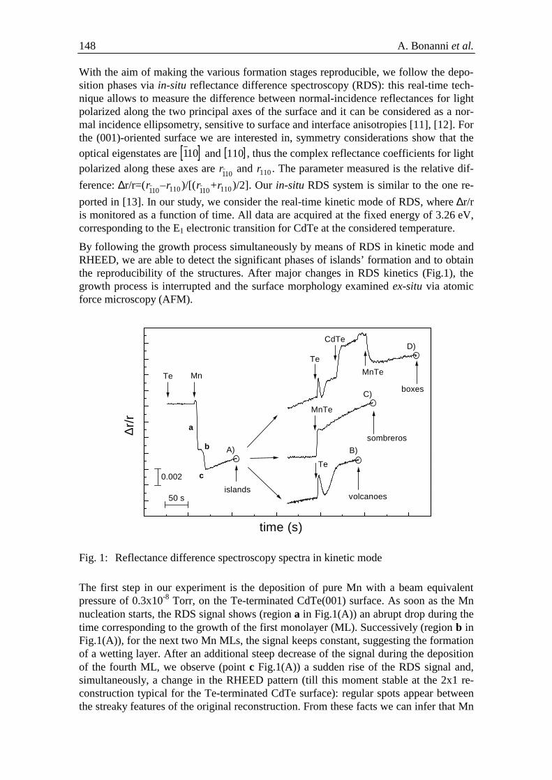
148 A. Bonanni et al.
With the aim of making the various formation stages reproducible, we follow the depo-sition phases via in-situ reflectance difference spectroscopy (RDS): this real-time tech-nique allows to measure the difference between normal-incidence reflectances for lightpolarized along the two principal axes of the surface and it can be considered as a nor-mal incidence ellipsometry, sensitive to surface and interface anisotropies [11], [12]. Forthe (001)-oriented surface we are interested in, symmetry considerations show that the
optical eigenstates are [ ]110 and [ ]110 , thus the complex reflectance coefficients for lightpolarized along these axes are r
110 and r110. The parameter measured is the relative dif-
ference: ∆r/r=(r110
–r110)/[( r110
+r110)/2]. Our in-situ RDS system is similar to the one re-
ported in [13]. In our study, we consider the real-time kinetic mode of RDS, where ∆r/ris monitored as a function of time. All data are acquired at the fixed energy of 3.26 eV,corresponding to the E1 electronic transition for CdTe at the considered temperature.
By following the growth process simultaneously by means of RDS in kinetic mode andRHEED, we are able to detect the significant phases of islands’ formation and to obtainthe reproducibility of the structures. After major changes in RDS kinetics (Fig.1), thegrowth process is interrupted and the surface morphology examined ex-situ via atomicforce microscopy (AFM).
50 s
c
b
a
0.002
boxes
sombreros
volcanoesislands
MnTe
CdTe
Te
MnTe
Te
MnTe
B)
C)
D)
A)
∆ r/r
time (s)
Fig. 1: Reflectance difference spectroscopy spectra in kinetic mode
The first step in our experiment is the deposition of pure Mn with a beam equivalentpressure of 0.3x10⁻⁸ Torr, on the Te-terminated CdTe(001) surface. As soon as the Mnnucleation starts, the RDS signal shows (region a in Fig.1(A)) an abrupt drop during thetime corresponding to the growth of the first monolayer (ML). Successively (region b inFig.1(A)), for the next two Mn MLs, the signal keeps constant, suggesting the formationof a wetting layer. After an additional steep decrease of the signal during the depositionof the fourth ML, we observe (point c Fig.1(A)) a sudden rise of the RDS signal and,simultaneously, a change in the RHEED pattern (till this moment stable at the 2x1 re-construction typical for the Te-terminated CdTe surface): regular spots appear betweenthe streaky features of the original reconstruction. From these facts we can infer that Mn
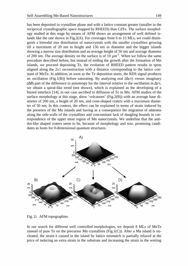
Self-Assembling Mn-Based Nanostructures 149
has been deposited in crystalline phase and with a lattice constant greater (smaller in thereciprocal crystallographic space mapped by RHEED) than CdTe. The surface morphol-ogy studied at this stage by means of AFM shows an arrangement of well defined is-lands like the one shown in Fig.2(A). For coverages from 6 to 15 MLs, we could distin-guish a bimodal size distribution of nanocrystals with the smaller crystallites growingtill a maximum of 20 nm in height and 150 nm in diameter and the bigger islandsshowing a narrow size distribution and an average height of 50 nm and average diameterof 200 nm. The average density on the surface is of 10 µm-2. When we follow the sameprocedure described before, but instead of ending the growth after the formation of Mnislands, we proceed depositing Te, the evolution of RHEED pattern results in spotsaligned along the 2x1 reconstruction with a distance corresponding to the lattice con-stant of MnTe. In addition, as soon as the Te deposition starts, the RDS signal producesan oscillation (Fig.1(B)) before saturating. By analyzing real (∆r/r) versus imaginary(∆θ) part of the difference in anisotropy for the interval relative to the oscillation in ∆r/r,we obtain a spiral-like trend (not shown), which is explained as the developing of aburied interface [14], in our case ascribed to diffusion of Te in Mn. AFM studies of thesurface morphology at this stage, show ‘volcanoes’ (Fig.2(B)) with an average base di-ameter of 200 nm, a height of 20 nm, and cone-shaped craters with a maximum diame-ter of 50 nm. In this context, the effect can be explained in terms of strain induced bythe presence of the Mn islands and having as a consequence the migration of adatomsalong the side-walls of the crystallites and concomitant lack of dangling bounds in cor-respondence of the upper most region of Mn nanocrystals. We underline that the anti-dot-like shaped craters seem to be, because of morphology and size, promising candi-dates as hosts for 0-dimensional quantum structures.
Fig. 2: AFM topographies.
In our search for different well controlled morphologies, we deposit 8 MLs of MnTeinstead of pure Te on the precursor Mn crystallites (Fig.1(C)). After a Mn island is nu-cleated, the strain ε caused in the island by lattice mismatch is partially relaxed at theprice of inducing an extra strain in the substrate and increasing the strain in the wetting
150 A. Bonanni et al.
layer near the crystallite edge. Therefore, adatoms deposited on the wetted surface willhave to overcome an energy barrier ∆µs before they can attach to the island [15]. Duringsuccessive growth, the evolution of the morphology is also influenced kinetically bysurface stress, since adatoms tend to diffuse on the surface away from sites with highstrain [16]. The strain concentration at the island edge increases monotonically with theisland size; when it exceeds a critical value, the free energy for atoms to occupy a posi-tion at the island edge may become higher than that for atoms to occupy a crystal-lographically unusual, but less strained site [15]. These considerations explain why thegrowth of MnTe is hampered at the edges of the crystallites and tends to develop farfrom the borders of precursor Mn islands and generate the ‘sombrero’-like featuresshown in Fig.2(C).
Finally, after the deposition of Te and successive 15 MLs of CdTe followed by 8 MLs ofMnTe on the precursor Mn island (Fig.1(D)), we obtain a quasi-periodic arrangement ofequally shaped ‘boxes’ with very regular squared bases of 200 nm x 200 nm and heightof 20 nm (Fig.2(D)). Despite the presence of these features on the surface, the RHEEDpattern appears streaky 2x1, due to the high density and the ML-scale flatness of theislands’ top. The structures show the tendency to arrange along the [100] and [010]crystallographic directions, as predicted [17] for a stable array of islands on a (001)-oriented surface. Thermodynamic calculations have shown that after an island is nucle-ated the system free energy decreases monotonically with increasing island size [10].Thus, a free energy minimum at a certain size is required in order to explain why ob-served islands’ sizes tend to be so uniform. One should bear in mind not only the ener-getics, but also the kinetics, which implies that the islands’ height grows slowly com-pared to the basis and may be treated as roughly constant. The kinetics can be incorpo-rated by minimizing the total island energy with respect to width and length of the crys-tallite keeping the height constant. The result is that, in thermodynamic limit, with highdensity of islands, they should grow until each nanocrystal is square-based. This mor-phology represents the optimal trade-off between surface energy and strain. In our casethe ‘boxes’, after reaching the squared-basis configuration, do not undergo further rip-ening and shape and basis size keep constant. Additional growth of MnTe leads to anincrease of the crystallite height.
3. ConclusionsIn conclusion, we achieved the reproducibility of self-assembling Mn-based nanocrys-tals, by monitoring in real time the subsequent stages of the growth process. The exten-sion to other material systems and growth techniques would be straightforward, the RDSbeing suitable for MBE as well as for non-ultra-high-vacuum systems like chemical va-por deposition (CVD) reactors.
References[1] D.Leonard, K.Pond, P.M.Petroff, Phys. Rev. B 50, 11687 (1994).
[2] A.Haury, A.Wasiela, A.Arnoult, J.Cibert, S.Tatarenko, T.Dietl, Y.Merled’Aubigné, Phys. Rev. Lett. 79, 511 (1997).
[3] S.A.Crooker, D.A.Tulchinsky, J.Levy, D.D. Awschalom, R.Garcia, N.Samarth,Phys. Rev. Lett. 75, 505 (1995).
Self-Assembling Mn-Based Nanostructures 151
[4] A.Bonanni, W.Heiß, G.Prechtl, D.Stifter, K.Hingerl, H.Sitter, Phys. Stat. Sol. (a)164, 331 (1997).
[5] H.Ulmer-Tuffigo, F.Kany, J.M.Hartmann, G.Feuillet, J.L.Pautrat, Solid-StateComm. 40, 75 (1996).
[6] T.Mizokawa, A.Fujimori Phys. Rev. B 56, 6669 (1997) and references therein.
[7] Jing Shi, S.Gider, K.Babcock, D.D.Awschalom, Science 271, 937 (1996).
[8] J.Tersoff, F.K.LeGoues, Phys. Rev. Lett. 72, 3570 (1994).
[9] W.Yu, A. Madhukar, Phys. Rev. Lett. 79, 905 (1997).
[10] T.M.Giebultowicz, N.Samarth, H.Luo, J.K.Furdyna, P.Klosowski, J.J.Rhyne, Phys.Rev. B 46, 12076 (1992).
[11] D.E.Aspnes, A.A.Studna, Phys. Rev. Lett. 54, 1956 (1985).
[12] T.Jasuda, K.Kimura, S.Miwa, L.H.Kuo, C.G.Jin, K.Tanaka, T.Yao, Phys. Rev.Lett. 77, 326 (1996).
[13] O.Acher, B.Drévillon, Rev. Sci. Instrum. 63, 5332 (1992).
[14] B.A.Phillips, I.Kamiya, K.Hingerl, L.T.Florez, D.E.Aspnes, S.Mahajan,J.P.Harbison, Phys. Rev. Lett. 74, 3640 (1995).
[15] Y.Chen, J.Washburn, Phys. Rev. Lett. 77, 4046 (1996).
[16] Q.Xie, P.Chen, A.Madhrukar, Appl. Phys. Lett. 65, 2051 (1994).
[17] V.A.Shuchukin, N.N.Ledentsof, P.S.Kop’ev, D.Bimberg, Phys. Rev. Lett. 75, 2968(1995).

The Society for Microelectronics – Annual Report 1999 153
Molecular Beam Epitaxy Growth of 3DQuantum Dot Crystals
M. Pinczolits, G. Springholz, V. Holy, and G. BauerInstitut für Halbleiterphysik, Johannes Kepler Universität,
A-4040 Linz, AustriaH. H Kang and L. Salamanca-Riba
Material and Nuclear Engineering Department, University of Maryland,College Park, USA
The self-organization of pyramidal PbSe islands that spontaneously form duringstrained-layer epitaxial growth of PbSe/PbEuTe superlattices results in the formationof three-dimensional quantum-dot crystals. In these crystals, the dots are arranged ina trigonal lattice with a face-centered cubic (fcc)-like ABCABC... stacking sequence.As shown by theoretical calculations, the elastic anisotropy in these artificial dotcrystals acts in a manner similar to that of the directed chemical bonds of crystallinesolids.
1. IntroductionThe spontaneous formation of nano-scale three dimensional (3D) islands duringstrained-layer heteroepitaxy has recently emerged as novel technique for fabrication ofself-assembled quantum dots. It is based on the fundamental instability of highlystrained surfaces that leads to nucleation of coherent islands on the surface after com-pletion of the wetting layer. In multilayer structures, the buried dots tend to influence thedot nucleation in the subsequent layers due to long range elastic interactions. This usu-ally results in a vertical alignment of the dots, but may also lead to an ordering in thelateral direction. This could lead to improved quantum dot size homogenities, which isof crucial importance for device applications.
2. Experimental ResultsIn the present work, we have investigated the evolution of vertical and lateral correla-tions in self-assembled PbSe/PbEuTe quantum dot superlattices grown by molecularbeam epitaxy on PbTe (111) surfaces. In these superlattices, the composition of the ter-nary layer was adjusted to achieve a complete strain symmetrization of the superlatticestack, which allows the growth of an unlimited number of superlattice periods withoutmisfit dislocation formation. Atomic force microscopy (AFM) investigations (Fig. 1)indicate a nearly perfect hexagonal ordering of the PbSe quantum dots within the layersas the number of superlattice periods increases. From high resolution x-ray diffractionand transmission electron microscopy (TEM) studies we find that the vertical correlationof the dots is not parallel but inclined with respect to the growth direction. As a conse-quence, an ABCABC... vertical dot stacking sequence is formed, similar to the stackingof the closely packed (111) planes in fcc-lattices.
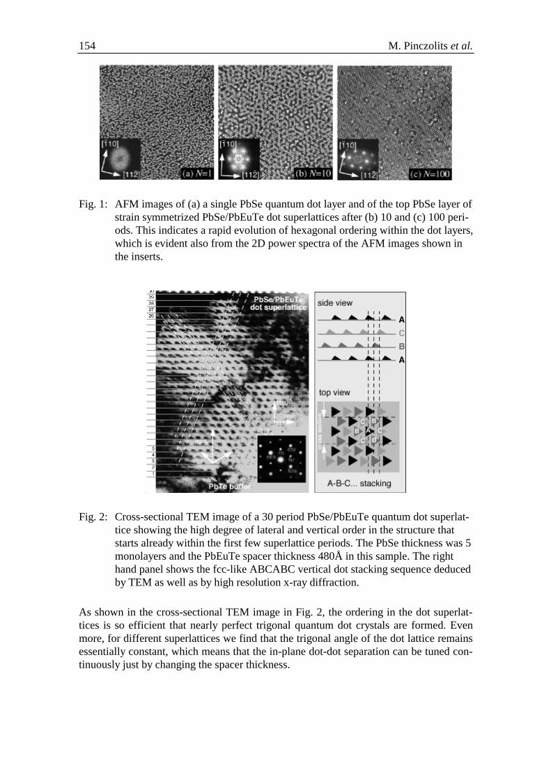
154 M. Pinczolits et al.
Fig. 1: AFM images of (a) a single PbSe quantum dot layer and of the top PbSe layer ofstrain symmetrized PbSe/PbEuTe dot superlattices after (b) 10 and (c) 100 peri-ods. This indicates a rapid evolution of hexagonal ordering within the dot layers,which is evident also from the 2D power spectra of the AFM images shown inthe inserts.
Fig. 2: Cross-sectional TEM image of a 30 period PbSe/PbEuTe quantum dot superlat-tice showing the high degree of lateral and vertical order in the structure thatstarts already within the first few superlattice periods. The PbSe thickness was 5monolayers and the PbEuTe spacer thickness 480Å in this sample. The righthand panel shows the fcc-like ABCABC vertical dot stacking sequence deducedby TEM as well as by high resolution x-ray diffraction.
As shown in the cross-sectional TEM image in Fig. 2, the ordering in the dot superlat-tices is so efficient that nearly perfect trigonal quantum dot crystals are formed. Evenmore, for different superlattices we find that the trigonal angle of the dot lattice remainsessentially constant, which means that the in-plane dot-dot separation can be tuned con-tinuously just by changing the spacer thickness.
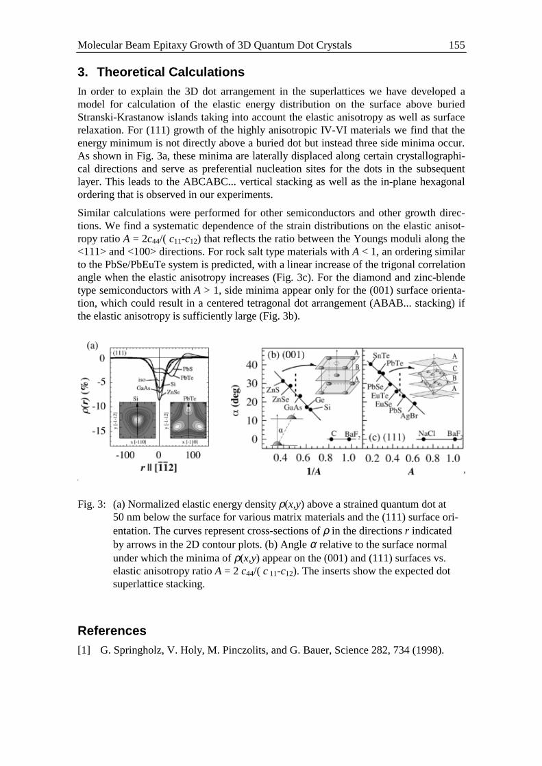
Molecular Beam Epitaxy Growth of 3D Quantum Dot Crystals 155
3. Theoretical CalculationsIn order to explain the 3D dot arrangement in the superlattices we have developed amodel for calculation of the elastic energy distribution on the surface above buriedStranski-Krastanow islands taking into account the elastic anisotropy as well as surfacerelaxation. For (111) growth of the highly anisotropic IV-VI materials we find that theenergy minimum is not directly above a buried dot but instead three side minima occur.As shown in Fig. 3a, these minima are laterally displaced along certain crystallographi-cal directions and serve as preferential nucleation sites for the dots in the subsequentlayer. This leads to the ABCABC... vertical stacking as well as the in-plane hexagonalordering that is observed in our experiments.
Similar calculations were performed for other semiconductors and other growth direc-tions. We find a systematic dependence of the strain distributions on the elastic anisot-ropy ratio A = 2c44/( c11-c12) that reflects the ratio between the Youngs moduli along the<111> and <100> directions. For rock salt type materials with A < 1, an ordering similarto the PbSe/PbEuTe system is predicted, with a linear increase of the trigonal correlationangle when the elastic anisotropy increases (Fig. 3c). For the diamond and zinc-blendetype semiconductors with A > 1, side minima appear only for the (001) surface orienta-tion, which could result in a centered tetragonal dot arrangement (ABAB... stacking) ifthe elastic anisotropy is sufficiently large (Fig. 3b).
Fig. 3: (a) Normalized elastic energy density ρ(x,y) above a strained quantum dot at50 nm below the surface for various matrix materials and the (111) surface ori-entation. The curves represent cross-sections of ρ in the directions r indicatedby arrows in the 2D contour plots. (b) Angle α relative to the surface normalunder which the minima of ρ(x,y) appear on the (001) and (111) surfaces vs.elastic anisotropy ratio A = 2 c44/( c 11-c12). The inserts show the expected dotsuperlattice stacking.
References[1] G. Springholz, V. Holy, M. Pinczolits, and G. Bauer, Science 282, 734 (1998).


The Society for Microelectronics – Annual Report 1999 157
Appendix

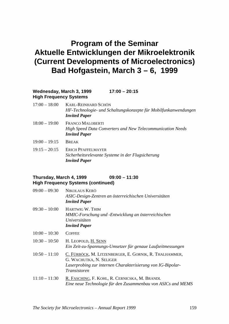
The Society for Microelectronics – Annual Report 1999 159
Program of the SeminarAktuelle Entwicklungen der Mikroelektronik(Current Developments of Microelectronics)
Bad Hofgastein, March 3 – 6, 1999
Wednesday, March 3, 1999 17:00 – 20:15High Frequency Systems
17:00 – 18:00 KARL-REINHARD SCHÖN
HF-Technologie- und Schaltungskonzepte für MobilfunkanwendungenInvited Paper
18:00 – 19:00 FRANCO MALOBERTI
High Speed Data Converters and New Telecommunication NeedsInvited Paper
19:00 – 19:15 BREAK
19:15 – 20:15 ERICH PFAFFELMAYER
Sicherheitsrelevante Systeme in der FlugsicherungInvited Paper
Thursday, March 4, 1999 09:00 – 11:30High Frequency Systems (continued)
09:00 – 09:30 NIKOLAUS KERÖ
ASIC-Design-Zentren an österreichischen UniversitätenInvited Paper
09:30 – 10:00 HARTWIG W. THIM
MMIC-Forschung und -Entwicklung an österreichischenUniversitätenInvited Paper
10:00 – 10:30 COFFEE
10:30 – 10:50 H. LEOPOLD, H. SENN
Ein Zeit-zu-Spannungs-Umsetzer für genaue Laufzeitmessungen
10:50 – 11:10 C. FÜRBÖCK, M. LITZENBERGER, E. GORNIK, R. THALHAMMER ,G. WACHUTKA, N. SELIGER
Laserprobing zur internen Charakterisierung von IG-Bipolar-Transistoren
11:10 – 11:30 R. FASCHING, F. KOHL, R. CERNICSKA, M. BRANDL
Eine neue Technologie für den Zusammenbau von ASICs and MEMS
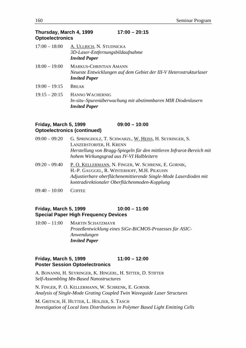
160 Seminar Program
Thursday, March 4, 1999 17:00 – 20:15Optoelectronics
17:00 – 18:00 A. ULLRICH, N. STUDNICKA
3D-Laser-EntfernungsbildaufnahmeInvited Paper
18:00 – 19:00 MARKUS-CHRISTIAN AMANN
Neueste Entwicklungen auf dem Gebiet der III-V HeterostrukturlaserInvited Paper
19:00 – 19:15 BREAK
19:15 – 20:15 HANNO WACHERNIG
In-situ–Spurenüberwachung mit abstimmbaren MIR DiodenlasernInvited Paper
Friday, March 5, 1999 09:00 – 10:00Optoelectronics (continued)
09:00 – 09:20 G. SPRINGHOLZ, T. SCHWARZL, W. HEISS, H. SEYRINGER, S.LANZERSTORFER, H. KRENN
Herstellung von Bragg-Spiegeln für den mittleren Infrarot-Bereich mithohem Wirkungsgrad aus IV-VI Halbleitern
09:20 – 09:40 P. O. KELLERMANN, N. FINGER, W. SCHRENK, E. GORNIK,H.-P. GAUGGEL, R. WINTERHOFF, M.H. PILKUHN
Adjustierbare oberflächenemittierende Single-Mode Laserdioden mitkontradirektionaler Oberflächenmoden-Kopplung
09:40 – 10:00 COFFEE
Friday, March 5, 1999 10:00 – 11:00Special Paper High Frequency Devices
10:00 – 11:00 MARTIN SCHATZMAYR
Prozeßentwicklung eines SiGe-BiCMOS-Prozesses für ASIC-AnwendungenInvited Paper
Friday, March 5, 1999 11:00 – 12:00Poster Session Optoelectronics
A. BONANNI, H. SEYRINGER, K. HINGERL, H. SITTER, D. STIFTER
Self-Assembling Mn-Based Nanostructures
N. FINGER, P. O. KELLERMANN, W. SCHRENK, E. GORNIK
Analysis of Single-Mode Grating Coupled Twin Waveguide Laser Structures
M. GRITSCH, H. HUTTER, L. HOLZER, S. TASCH
Investigation of Local Ions Distributions in Polymer Based Light Emitting Cells
Seminar Program 161
W. HEISS, G. PRECHTL, D. STIFTER, H. SITTER, G. SPRINGHOLZ, L. TOTH
ZnCdSe/ZnSe Quantum Wires by Epitaxy on Prepatterned GaAs Substrate
L. HVOZDARA, S. GIANORDOLI, G. STRASSER, K. UNTERRAINER, E. GORNIK
GaAs/AlGaAs Based Intersubband and Interminiband Mid-Infrared Emitters
S. LANZERSTORFER, M. STEPIKHOVA, H. PREIER, L. PALMETSHOFER, W. JANTSCH
Light Generation by Er in Si Related Materials
T. MAIER, G. STRASSER, E. GORNIK
GaAs VCSELs with Dielectric Si3N4/SiO2 Mirrors
S. MUSSER, H. HUTTER, P. WILHARTITZ
Determination of Trace Element Distribution in Cr Sputter Targets by 3-d SIMS
W. SCHRENK, N. FINGER, T. MAIER, P. O. KELLERMANN, G. STRASSER, E. GORNIK
GaAs/AlGaAs/InGaAs Bandgap Lasers — From DH Lasers to VCSELs
J. ULRICH, R. ZOBL, K. UNTERRAINER, G. STRASSER, E. GORNIK, K. D. MARANOWSKI,A. C. GOSSARD
Far-Infrared Electroluminescence in Parabolic Quantum Wells
Friday, March 5, 1999 17:00 – 20:15High Frequency Devices
17:00 – 18:00 HARTMUT PRESTING, ULF KÖNIG
Stand und Anwendungen von Si/SiGe-Hochfrequenz- undOptoelektronik-BauelementenInvited Paper
18:00 – 19:00 ANDREAS SCHÜPPEN
Stand der Prozeßentwicklung und Markteinführung des SiGe-HBTInvited Paper
19:00 – 19:15 BREAK
19:15 – 20:15 HARTMUT KAPUSTA
GaAs-MMIC Design-Aspekte für MassenproduktionInvited Paper
Saturday, March 6, 1999 09:00 – 11:00High Frequency Devices (continued)
09:00 – 10:00 FRIEDRICH SCHÄFFLER
Hoch- und Höchstfrequenz-Bauelemententwicklung anösterreichischen UniversitätenInvited Paper
10:00 – 10:20 COFFEE
10:20 – 10:40 K. WIESAUER, G. SPRINGHOLZ
Nanolithographie für Halbleiter-Nanostrukturen unter Verwendungvon Rasterkraftmikroskopie
162 Seminar Program
10:40 – 11:00 A. LUGSTEIN, H. WANZENBÖCK, E. BERTAGNOLLI
Fokussierte Ionenstrahlen, eine neue Technologie für dieMikrostrukturierung im Bereich unter 100 Nanometern
Saturday, March 6, 1999 11:00 – 12:00Poster Session High Frequency Devices
R. HEER, J. SMOLINER, G. STRASSER, E. GORNIK
Enhanced Energy Resolution in Ballistic Electron Emission Microscopy Through InAsBase Layers
C. RAUCH, G. STRASSER, AND E. GORNIK
Onset of Scattering Induced Miniband Transport
N. SANDERSFELD, H. SEYRINGER, G. STEINBACHER, L. PALMETSHOFER, S. ZERLAUTH, F.SCHÄFFLER
Modulation Doped Si/Si1-xGex-Field-Effect Transistors
C. SCHELLING, G. SPRINGHOLZ, F. SCHÄFFLER
Growth Instabilities in Si Homoepitaxy
TH. SCHWARZL, W. HEISS, G. KOCHER-OBERLEHNER, G. SPRINGHOLZ
CH4/H2 Plasma Etching of IV-VI Semiconductors
H. SEYRINGER, B. FÜNFSTÜCK, F. SCHÄFFLER
Electron Beam Lithography of Nanostructures
J. STANGL, Y. ZHUANG, G. BAUER C. ROSENBLAD, H. VON KÄNEL
Fast Growth Method for the Fabrication of Modulation Doped Si/SiGe Field EffectTransistors
Y. ZHUANG, P. MIKULIK , V. HOLÝ, G. BAUER, R. HAMMOND, T. E. WHALL ,E. H. C. PARKER
Si/SiGe Layers on Patterned Substrates for MODFET Applications
The Society for Microelectronics – Annual Report 1999 163
The Society’s Managing Committee andAddress
President:Univ.Prof. Dr. Erich GORNIK
TU Wien, Institut für Festkörperelektronik
First Vice-President:Mag. Miron PASSWEG
Bundesarbeitskammer
Second Vice-President:Univ.Prof. Dr. Günther BAUER
Universität Linz, Institut für Halbleiterphysik
Board:Dr. Wolfgang ATTWENGER
ÖFZ Seibersdorf
Univ.Prof. Dr. Wolfgang FALLMANN
TU Wien, Institut für Angewandte Elektronik und Quantenelektronik
Univ.Prof. Dr. Helmut HEINRICH
Universität Linz, Institut für Experimentalphysik
Dipl.-Ing. Gerhard KRAINZ
Wirtschaftskammer Österreich
Univ.Prof. Dr. Hans LEOPOLD
TU Graz, Institut für Elektronik
Univ.Prof. Dr. Fritz PASCHKE
TU Wien, Institut für Angewandte Elektronik und Quantenelektronik
Dr. Robert SCHAWARZ
TU Wien, Institut für Angewandte Elektronik und Quantenelektronik
Univ.Prof. Dr. Arnold SCHMIDT
TU Wien, Institut für Angewandte Elektronik und Quantenelektronik
Univ.Prof. Dr. Siegfried SELBERHERR
TU Wien, Institut für Mikroelektronik

164 The Society's Managing Committee
Secretary-General:A.o. Univ.Prof. Dr. Karl RIEDLING
TU Wien, Institut für Angewandte Elektronik und Quantenelektronik
Administration:Claudia BENEDELA
Address:Gesellschaft für Mikroelektronikc/o Technische Universität WienInstitut für Angewandte Elektronik und QuantenelektronikGußhausstraße 27-29/359, A-1040 Wien
Phone: +43-1-588 01-35947
Fax: +43-1-588 01-35999
Mail: [email protected]
WWW: http://www.iaee.tuwien.ac.at/gme/