Embed Size (px)
Citation preview
Simulation of Medical Irradiationand
X-Ray Detector Signals
Der Naturwissenschaftlichen Fakultatder Friedrich-Alexander-Universitat
Erlangen-Nurnberg
zur
Erlangung des Doktorgrades Dr. rer. nat.
vorgelegt von
Bjorn Kreisleraus Frankfurt am Main

Als Dissertation genehmigtvon der Naturwissenschaftlichen Fakultatder Friedrich-Alexander Universitat Erlangen-Nurnberg
Tag der mundlichen Prufung: 8. Februar 2010Vorsitzender derPromotionskommission: Prof. Dr. Eberhard BanschErstberichterstatterin: Prof. Dr. Gisela AntonZweitberichterstatter: Prof. Dr. Stanislav Pospisil


Contents
Introduction 1
I Semiconductor Detector Signals 5
1 Basics of the Signal Calculation for Semiconductor X-Ray Detectors 71.1 X-Ray Semiconductor Detectors . . . . . . . . . . . . . . . . . . . . . . . 71.2 Electric Fields in Matter . . . . . . . . . . . . . . . . . . . . . . . . . . . . 8
1.2.1 Bias Field . . . . . . . . . . . . . . . . . . . . . . . . . . . . . . . . 91.2.2 Weighting Field . . . . . . . . . . . . . . . . . . . . . . . . . . . . . 9
1.3 Charge Motion and Induced Currents . . . . . . . . . . . . . . . . . . . . 101.4 Adjoint Solution . . . . . . . . . . . . . . . . . . . . . . . . . . . . . . . . 121.5 Generalised Adjoint Solution . . . . . . . . . . . . . . . . . . . . . . . . . 14
2 Signal Simulation 152.1 Finite Element Simulation . . . . . . . . . . . . . . . . . . . . . . . . . . . 152.2 Static Electric Fields . . . . . . . . . . . . . . . . . . . . . . . . . . . . . . 162.3 Charge Motion and Electric Induction . . . . . . . . . . . . . . . . . . . . 162.4 Adjoint Solution and Charge Induction Map . . . . . . . . . . . . . . . . . 17
3 Results 213.1 Electric Fields . . . . . . . . . . . . . . . . . . . . . . . . . . . . . . . . . . 213.2 Currents and Collected Charges . . . . . . . . . . . . . . . . . . . . . . . . 24
3.2.1 Different Bias Voltages . . . . . . . . . . . . . . . . . . . . . . . . . 273.2.2 Different Initial Charge . . . . . . . . . . . . . . . . . . . . . . . . 293.2.3 Different Pixel Pitch . . . . . . . . . . . . . . . . . . . . . . . . . . 323.2.4 Different Pixel Electrodes . . . . . . . . . . . . . . . . . . . . . . . 32
3.3 Steering Grid Geometry . . . . . . . . . . . . . . . . . . . . . . . . . . . . 34
4 Summary and Discussion of Part I 37
II Radiation Field of a Medical Linear Accelerator 41
5 Basics of Medical Irradiation 435.1 Dose Definition . . . . . . . . . . . . . . . . . . . . . . . . . . . . . . . . . 435.2 Tumour Treatment . . . . . . . . . . . . . . . . . . . . . . . . . . . . . . . 44
5.2.1 Photons vs. Electrons . . . . . . . . . . . . . . . . . . . . . . . . . 465.2.2 Multifield Irradiation . . . . . . . . . . . . . . . . . . . . . . . . . . 48

6 Simulation Setup 496.1 Basic Setup . . . . . . . . . . . . . . . . . . . . . . . . . . . . . . . . . . . 496.2 Electron Irradiation . . . . . . . . . . . . . . . . . . . . . . . . . . . . . . 506.3 Photon Irradiation . . . . . . . . . . . . . . . . . . . . . . . . . . . . . . . 526.4 Data Analysis . . . . . . . . . . . . . . . . . . . . . . . . . . . . . . . . . . 52
7 Results 557.1 Electron Irradiation . . . . . . . . . . . . . . . . . . . . . . . . . . . . . . 55
7.1.1 Validation of the Simulation . . . . . . . . . . . . . . . . . . . . . . 557.1.2 Analysis of Parameters . . . . . . . . . . . . . . . . . . . . . . . . . 57
7.2 Photon Irradiation . . . . . . . . . . . . . . . . . . . . . . . . . . . . . . . 65
8 Summary and Discussion of Part II 71
Summary 73
Zusammenfassung 75
Bibliography 76
Acknowledgements 81


Introduction
The World Health Organisation (WHO) runs a program to classify the causes of mortalitycalled the International Statistical Classification of Diseases (ICD). This classification hasits origins in the 1850s and has been part of the WHO since 1948 when the sixth versionof the ICD was published. The latest version (ICD-10, Version 2007 ) outlines two majormortality reasons in the member states of the WHO: Diseases of the circulatory systemand Neoplasms.In modern societies, the early diagnosis of tumours is one aim of the routine medicalchecks. But even in the case of a diagnosis, the treatment of tumours requires deepermedical and physical knowledge. A case dependent combination of surgery, chemother-apy and irradation offers the best chance to cure the disease. In chemotherapy, drugmedication is used to reduce the tumour size and growth, but the complete body has tocope with the drug. Irradiation medicates the tumour cells by depositing energy insidethe tumour tissue, destroying the DNA (desoxyribonucleic acid - the long term carrier ofgenetic instructions) inside the cell nucleus and thereby forcing the cells into apoptosis.The irradiation is possible with different sorts of particles: electrons, photons, protons orheavy ions. The choice between the different irradiation options is guided by the need toprotect the surrounding healthy tissue from dose deposition. As facilities for proton orheavy ion irradiation are rather large and expensive and not suitable for all cases, mostirradiation is performed with photons and electrons.Electron or photon beams are generated by accelerating electrons in a linear acceleratorand then widening and flattening the beam by scattering foils. In the case of photon irra-diation, a target is part of the beamline where photons are generated by Bremsstrahlung.The beam shaping is performed by collimation units which confine the beam laterally.For electron irradiation, the collimation is additionally performed by applicators to limitthe electron beam dimensions close to the patient to reduce the divergency of the beam.The irradiation of the tumour tissue is planned based on computed tomography datausing simplified Monte-Carlo tools. The beam input data for these planning systems aregained by measurements of the beam characteristics. The beam shape and homogeneityare commonly measured by films and dose chambers, which are both indirect measures asthe deposited energy inside a given small volume is determined. Thereby, the informationof the spectral distribution of the beam is lost, although this knowledge would be inter-esting as the penetration depth varies strongly with the initial energy. The measurementof the spatial and spectral distribution of the beam is technically difficult because the fluxinside the beam is very large.The complete beam characteristics can therefore only be acquired by a detailed simula-tion or by a new detector which can handle the flux in the beam. State of the art X-raydetectors are based on a semiconductor sensor layer which converts the incoming flux ofphotons (or high energy electrons) into electron hole pairs, which are then translated intoan electronic signal. The separation of single interactions of the incoming particles can be
1
achieved. The signal shape and deposited energy per electron can be used to determinethe spectral information of the incoming beam. Furthermore, if the sensor is pixelated,the detection can even be carried out with a spatial resolution. Nonetheless, the exactknowledge of the signals which are generated by the incoming beam is essential for thedesign of a detector.The following work is separated in two main parts. In the first part, the design of adetector for X-rays is the central point. The signal generation after the interaction of anX-ray photon in the sensor will be explained. The influence of the geometrical dimensionsand applied voltages is investigated and can be used to provide a guide for the design ofthe readout electronics. In the second part, the main focus is on the medical irradiation.Beginning with the basics of dosimetry and tumour treatment, the simulation of a medicalirradiation system will be presented followed by the analysis of some parameters for theunderstanding of the systematics of the medical irradiation.Together, both parts can show a way to improve the quality of medical irradiation. Theenhanced knowledge on the beam parameters can be compared to accurate measure-ments with possible new detectors. And the advanced development of medical irradiationsystems will improve by making use of simulations which offers an elegant way for opti-misation.


Part I
Semiconductor Detector Signals
5


1 Basics of the Signal Calculation forSemiconductor X-Ray Detectors
Digital state of the art X-ray detection is realised either by scintillation or semiconductorsystems. In comparison to the analog film (or digital storage phosphor) systems, thedigital detection systems show a linear response over a wide energy and intensity rangeand can be used in multi imaging devices like computed tomography.Scintillation and semiconductor systems have a fundamental difference: the X-rays insidea scintillator system are detected indirectly by converting the X-rays into visible lightand then taking an image of this visible light with a charge-coupled device camera. Thefollowing work will focus on the direct detection with a semicondutor sensor layer wherethe X-rays are immediately converted into charges which are then transferred to thereadout electronics.The charge drift by a static electric bias field can be described by the continuity equation.The signal which enters the electronics is induced during the charge motion, and thischarge induction process can be calculated using the so called pseudo electric weightingfield. The indicated electric fields, the motion process and the charge induction calculationwill be presented in the following chapter. The chapter will start with a short introductioninto semiconductor X-ray detector design and operating mode.
1.1 X-Ray Semiconductor Detectors
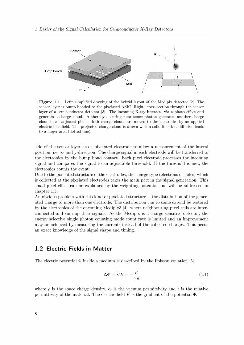
Digital X-ray detection can be divided into two major steps: energy transfer from theincoming X-ray photons to a sensor volume and collection of the generated charge signalby a dedicated electronics. These two steps can be very clearly observed when looking atthe hybrid X-ray detector Medipix [1], which is drawn in the left of figure 1.1. A semi-conductor sensor layer is bump bonded to the Medipix ASIC pixel by pixel. Thereforeenergy transfer takes place in the sensor layer, but signal processing is performed in theelectronics below.The dimensions of the detector are rather small: each square pixel has an edge lengthof 55µm, and there are 256 × 256 pixels per sensor, which leads to a sensitive area of1.98 cm2. The bump bonding can be altered in a way that not every electronic pixel isconnected to the sensor layer. This leads to fewer but larger pixels as the area of theASIC is limited. An option to enlarge the sensitive area is to tile a larger area with morereadout ASICs. As the ASIC is three side buttable, a large sensitive area with a width of512 pixels can be constructed.In the right part of figure 1.1, a cross-section though a sensor layer is drawn. An incomingX-ray photon interacts with the sensor material and free charge carriers are generated.As a bias voltage is applied across the sensor layer, i.e. the z-direction, the charge carrierswill be separated and drift with respect to their charge sign towards the electrodes. One
7
1 Basics of the Signal Calculation for Semiconductor X-Ray Detectors
Figure 1.1 Left: simplified drawing of the hybrid layout of the Medipix detector [2]. Thesensor layer is bump bonded to the pixelated ASIC. Right: cross-section through the sensorlayer of a semiconductor detector [3]. The incoming X-ray interacts via a photo effect andgenerats a charge cloud. A thereby occuring fluoresence photon generates another chargecloud in an adjacent pixel. Both charge clouds are moved to the electrodes by an appliedelectric bias field. The projected charge cloud is drawn with a solid line, but diffusion leadsto a larger area (dotted line).
side of the sensor layer has a pixelated electrode to allow a measurement of the lateralposition, i.e. x- and y-direction. The charge signal in each electrode will be transferred tothe electronics by the bump bond contact. Each pixel electrode processes the incomingsignal and compares the signal to an adjustable threshold. If the threshold is met, theelectronics counts the event.Due to the pixelated structure of the electrodes, the charge type (electrons or holes) whichis collected at the pixelated electrodes takes the main part in the signal generation. Thissmall pixel effect can be explained by the weighting potential and will be addressed inchapter 1.3.An obvious problem with this kind of pixelated structure is the distribution of the gener-ated charge to more than one electrode. The distribution can to some extend be restoredby the electronics of the oncoming Medipix3 [4], where neighbouring pixel cells are inter-connected and sum up their signals. As the Medipix is a charge sensitive detector, theenergy selective single photon counting mode count rate is limited and an improvementmay be achieved by measuring the currents instead of the collected charges. This needsan exact knowledge of the signal shape and timing.
1.2 Electric Fields in Matter
The electric potential Φ inside a medium is described by the Poisson equation [5],
∆Φ = ~∇ ~E = − ρ
εε0(1.1)
where ρ is the space charge density, ε0 is the vacuum permittivity and ε is the relativepermittivity of the material. The electric field ~E is the gradient of the potential Φ.
8
1.2 Electric Fields in Matter
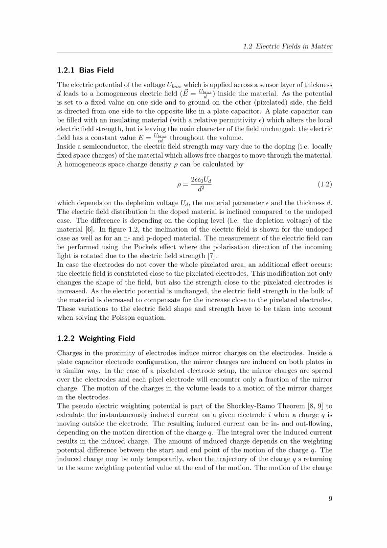
1.2.1 Bias Field
The electric potential of the voltage Ubias which is applied across a sensor layer of thicknessd leads to a homogeneous electric field ( ~E = Ubias
d ) inside the material. As the potentialis set to a fixed value on one side and to ground on the other (pixelated) side, the fieldis directed from one side to the opposite like in a plate capacitor. A plate capacitor canbe filled with an insulating material (with a relative permittivity ε) which alters the localelectric field strength, but is leaving the main character of the field unchanged: the electricfield has a constant value E = Ubias
εd throughout the volume.Inside a semiconductor, the electric field strength may vary due to the doping (i.e. locallyfixed space charges) of the material which allows free charges to move through the material.A homogeneous space charge density ρ can be calculated by
ρ =2εε0Udd2
(1.2)
which depends on the depletion voltage Ud, the material parameter ε and the thickness d.The electric field distribution in the doped material is inclined compared to the undopedcase. The difference is depending on the doping level (i.e. the depletion voltage) of thematerial [6]. In figure 1.2, the inclination of the electric field is shown for the undopedcase as well as for an n- and p-doped material. The measurement of the electric field canbe performed using the Pockels effect where the polarisation direction of the incominglight is rotated due to the electric field strength [7].In case the electrodes do not cover the whole pixelated area, an additional effect occurs:the electric field is constricted close to the pixelated electrodes. This modification not onlychanges the shape of the field, but also the strength close to the pixelated electrodes isincreased. As the electric potential is unchanged, the electric field strength in the bulk ofthe material is decreased to compensate for the increase close to the pixelated electrodes.These variations to the electric field shape and strength have to be taken into accountwhen solving the Poisson equation.
1.2.2 Weighting Field
Charges in the proximity of electrodes induce mirror charges on the electrodes. Inside aplate capacitor electrode configuration, the mirror charges are induced on both plates ina similar way. In the case of a pixelated electrode setup, the mirror charges are spreadover the electrodes and each pixel electrode will encounter only a fraction of the mirrorcharge. The motion of the charges in the volume leads to a motion of the mirror chargesin the electrodes.The pseudo electric weighting potential is part of the Shockley-Ramo Theorem [8, 9] tocalculate the instantaneously induced current on a given electrode i when a charge q ismoving outside the electrode. The resulting induced current can be in- and out-flowing,depending on the motion direction of the charge q. The integral over the induced currentresults in the induced charge. The amount of induced charge depends on the weightingpotential difference between the start and end point of the motion of the charge q. Theinduced charge may be only temporarily, when the trajectory of the charge q s returningto the same weighting potential value at the end of the motion. The motion of the charge
9
1 Basics of the Signal Calculation for Semiconductor X-Ray Detectors
d
bias dU +U
U
d
bias
d
bias dU −U
distance to anode0 d
E
Figure 1.2 Electric field strength E inside a semiconductor in a plate capacitor-like elec-trode configuration as a function of the distance to one plate. The electric field is calculatedby the bias voltage Ubias divided by the thickness of the semiconductor d. If a locally fixedspace charge is present in the semiconductor, the depletion voltage Ud changes the local elec-tric field strength. In the undoped case (solid line), the field strength is constant, in then-doped (dashed line) and p-doped (dotted line) case, the electric field strength is a linearfunction of the distance towards the electrode.
q depends on the actual electric field at the position of the charge, which means the mo-tion is not influenced by the weighting potential.The weighting potential can be obtained by solving the Poisson equation for a very sim-ple case: all electrodes are set to ground except the one of interest (electrode i) whichis set to unit potential. The volume is treated like vacuum, meaning no space chargeand no relative permittivity. The potiential includes values between zero and one. Theweighting field ~Wi is the gradient of the weighting potential calculated this way. Theweighting potential takes only geometrical aspects into account as no material propertiesare implemented in its calculation.
1.3 Charge Motion and Induced Currents
The electric bias field in the semiconductor sensor layer of an X-ray detector results in adrift of free charges. A charge cloud generated by an X-ray interaction will therefore driftwith respect to the electric field. This drift motion is superimposed by a gradient drivendiffusion and an inner electric repulsion.The charge motion neglecting replusion can be described by a continuity equation of thecharge concentration c
∂c
∂t− ~∇ · (D~∇c)− ~∇ · (c~v) = c0 (1.3)
10
1.3 Charge Motion and Induced Currents
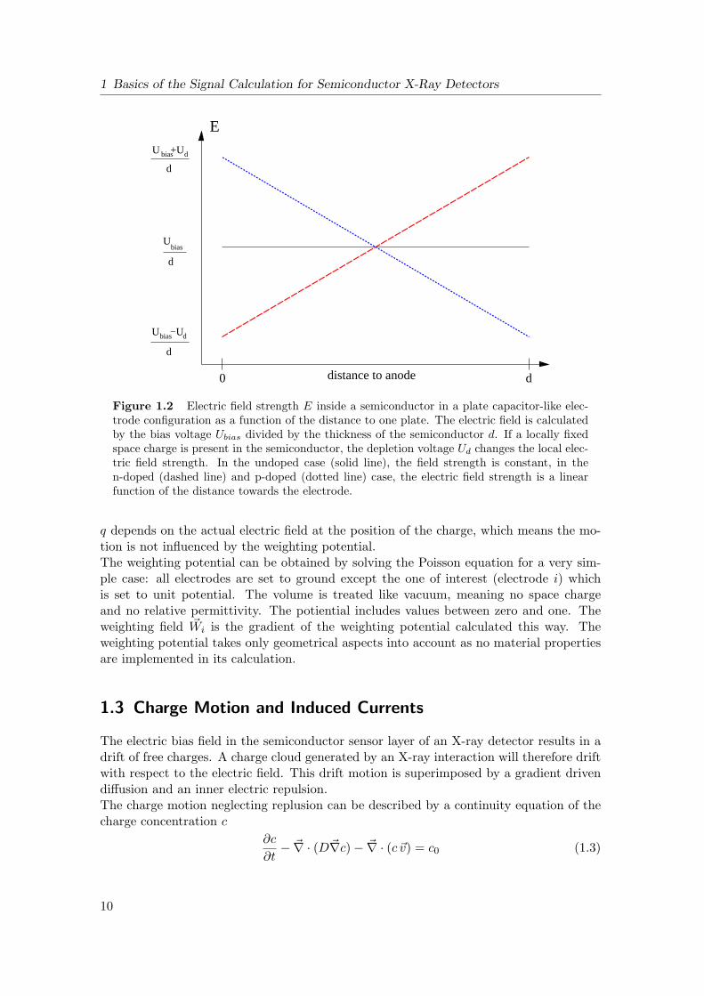
Figure 1.3 The electron drift velocity v inside CdTe is a function of the electric fieldstrength [10]. The slope of the function is the mobility µ, which is used to couple the motionwith the electric field.
where the drift velocity ~v is directly coupled to the electric field by the Einstein equation~v = µ~E. The mobility µ is a material parameter and depends on the electric field strength.In figure 1.3, the variation of the electron velocity in CdTe is plotted as a function of theelectric field. For other materials like silicon, the graph reaches a finite value for highelectric fields, i.e. a saturation velocity [11]. The isotropic diffusion is parametrised bythe coefficient D. The initial charge distribution c0 is placed at the interaction point ofthe incoming X-ray photon [12]. The transient flux ~F of this initial charge cloud is thenavailable,
~F (t) = c(t)~v +D ~∇c(t). (1.4)
The motion of the charge cloud (see figure 1.4) leads to a motion of the mirror chargesin the electrodes. The current in the electrodes, i.e. the motion of the mirror charges, isinduced during the motion of the charge cloud [13]. This effect can be described by theformalism proposed by Ramo [8]. The induction process makes use of the weighting field,as the geometrical setup of the sensor is coded in this pseudo electric field. The inducedelectric current I(t) on the ith electrode can be obtained by integrating the scalar productof the charge flux ~F (t) and the weighting field ~Wi of the ith electrode over the completesensor volume Vs,
I(t) =∫Vs
~F (t) · ~Wi dV. (1.5)
The collected charge on the electrode can be obtained by integrating the induced currentover the collection time. This calculation results in a current and charge signal on theelectrode of interest for a single interaction point of the X-ray photon. Signals from
11
1 Basics of the Signal Calculation for Semiconductor X-Ray Detectors
0 0,5 1 1,5distance from pixelated surface in mm
0
0,2
0,4
0,6
0,8
1
norm
alis
ed c
harg
e ca
rrie
r co
ncen
trat
ion
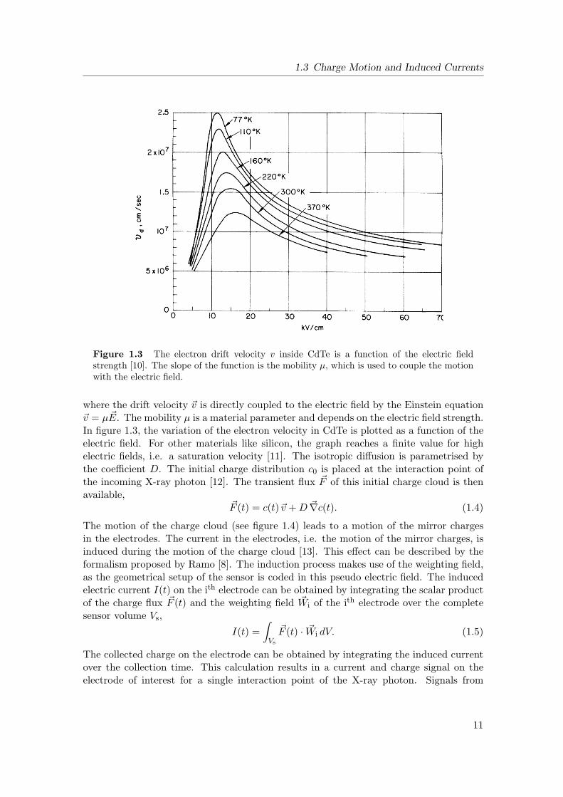
Figure 1.4 Stroboscopic view on a moving charge cloud with equal time stepping. Thecharge cloud starts on the right side and is moving to the left while the speed is decreasingdue to a decrease of the electric field strength.
adjacent electrodes can be obtained by integrating the charge flux multiplied by therespective weighting field of the adjacent electrode [14].The motion of the charge cloud has to be calculated for each possible starting point inthe sensor and the integration for each electrode has to be performed subsequently. Thisleads to a considerable computing time for a reasonable density of starting points.
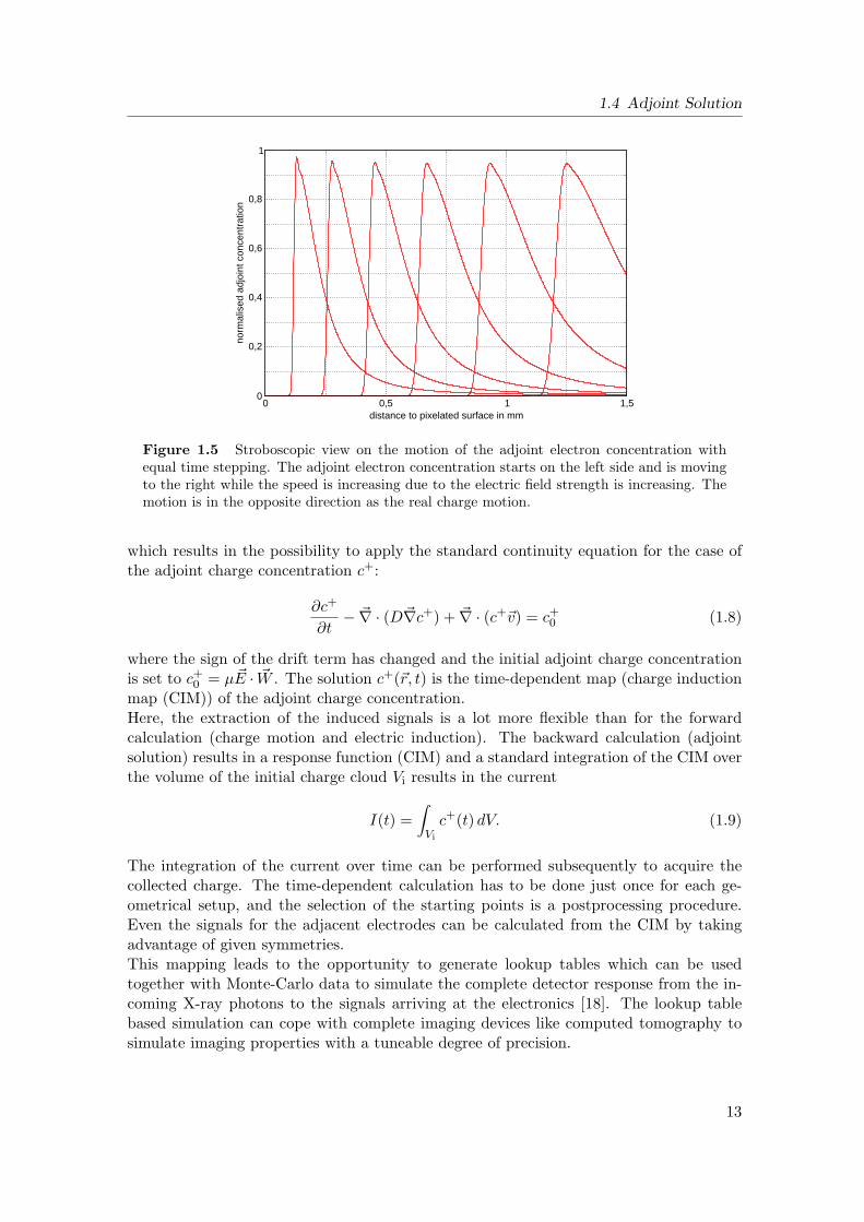
1.4 Adjoint Solution
To avoid this immense computing time, the adjoint solution was proposed by Pretty-man [15]. An adjoint continuity equation can be constructed as the charge carrier conti-nuity equation in the forward simulation involves linear operators [16, 17]. The continuityequation for the adjoint electron concentration c+ is given by
∂c+
∂t− ~∇ · (D~∇c+) + µ~E · ~∇c+ = c+0 (1.6)
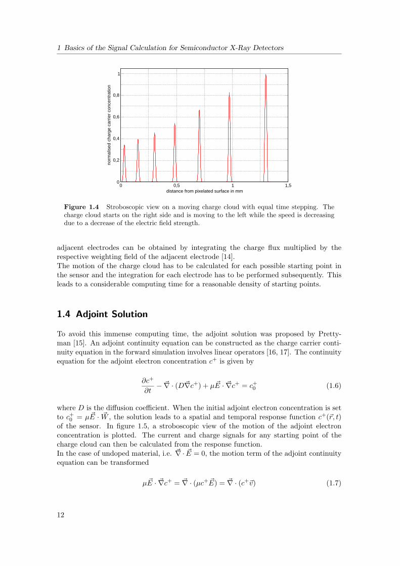
where D is the diffusion coefficient. When the initial adjoint electron concentration is setto c+0 = µ~E · ~W , the solution leads to a spatial and temporal response function c+(~r, t)of the sensor. In figure 1.5, a stroboscopic view of the motion of the adjoint electronconcentration is plotted. The current and charge signals for any starting point of thecharge cloud can then be calculated from the response function.In the case of undoped material, i.e. ~∇ · ~E = 0, the motion term of the adjoint continuityequation can be transformed
µ~E · ~∇c+ = ~∇ · (µc+ ~E) = ~∇ · (c+~v) (1.7)
12
1.4 Adjoint Solution
0 0,5 1 1,5distance to pixelated surface in mm
0
0,2
0,4
0,6
0,8
1
norm
alis
ed a
djoi
nt c
once
ntra
tion
Figure 1.5 Stroboscopic view on the motion of the adjoint electron concentration withequal time stepping. The adjoint electron concentration starts on the left side and is movingto the right while the speed is increasing due to the electric field strength is increasing. Themotion is in the opposite direction as the real charge motion.
which results in the possibility to apply the standard continuity equation for the case ofthe adjoint charge concentration c+:
∂c+
∂t− ~∇ · (D~∇c+) + ~∇ · (c+~v) = c+0 (1.8)
where the sign of the drift term has changed and the initial adjoint charge concentrationis set to c+0 = µ~E · ~W . The solution c+(~r, t) is the time-dependent map (charge inductionmap (CIM)) of the adjoint charge concentration.Here, the extraction of the induced signals is a lot more flexible than for the forwardcalculation (charge motion and electric induction). The backward calculation (adjointsolution) results in a response function (CIM) and a standard integration of the CIM overthe volume of the initial charge cloud Vi results in the current
I(t) =∫Vi
c+(t) dV. (1.9)
The integration of the current over time can be performed subsequently to acquire thecollected charge. The time-dependent calculation has to be done just once for each ge-ometrical setup, and the selection of the starting points is a postprocessing procedure.Even the signals for the adjacent electrodes can be calculated from the CIM by takingadvantage of given symmetries.This mapping leads to the opportunity to generate lookup tables which can be usedtogether with Monte-Carlo data to simulate the complete detector response from the in-coming X-ray photons to the signals arriving at the electronics [18]. The lookup tablebased simulation can cope with complete imaging devices like computed tomography tosimulate imaging properties with a tuneable degree of precision.
13

1 Basics of the Signal Calculation for Semiconductor X-Ray Detectors
1.5 Generalised Adjoint Solution
The main disadvantage of the adjoint solution is the restriction to undoped or only poorlydoped materials. State of the art semiconductor sensor materials like CdTe or CdZnTeare intrinsically doped to a level, which cannot be treated sufficiently with the previouslypresented method [15].The sensor layer of the hybrid X-ray detector Medipix which is investigated in the lab-oratory at the ECAP (Erlangen Centre for Astroparticle Physics) for spectral imagingpurposes is made of CdTe. The inhomogeneity of the electric field due to doping is notnegligible in this material. Therefore it was necessary to find a way to extend the simu-lation for this case.As the adjoint continuity equation (see equation (1.6)) is not affected by the inhomogene-ity of the electric field, the critical point is the transformation of the motion term [19].The correct propagation of the ~∇-operator in the motion term of the adjoint continuityequation leads to
µ~E · ~∇c+ = ~∇ · (µc+ ~E)− µc+~∇ · ~E = ~∇ · (c+~v)− µc+~∇ · ~E (1.10)
which is true even if the electric field has a spatial variation due to doping. The additionalterm vanishes in the case of no inhomogeneities. The restriction of the adjoint solutionto undoped material can thus be overcome by adding a term to the continuity equation[20],
δc+
δt− ~∇ · (D~∇c+) + ~∇ · (c+~v)− µc+~∇ ~E = c+0 . (1.11)
The equation is very similar to equation (1.8), but the additional term adjusts the in-tegral over the complete response function. The adjustment leads to a correction of theinduced current signal height, and therefore corrects the amount of collected charge. Thecompensation is not limited to homogeneous doping, it can cope with a locally variingdoping profile as well.The calculation of an induced signal I(t) is performed like for the standard adjoint solu-tion by integrating the CIM over the initial charge cloud volume Vi as in equation (1.9).The induced signals can again be integrated over time to get the collected charge.The generalised adjoint solution allows the generation of a CIM for doped semiconductorsensor materials. This is an important improvement for applying the method to detectorslike CdTe, which are needed for medical applications.
14
2 Signal Simulation
The transient motion of the charge concentration and of the adjoint charge concentrationare described by partial differential equations which can be solved numerically. Thecommercial finite element simulation tool COMSOL Multiphysics [21] was used for thispurpose.
2.1 Finite Element Simulation
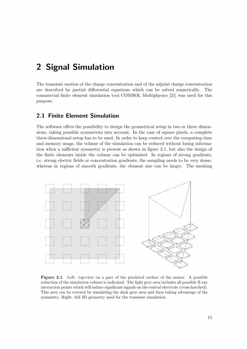
The software offers the possibility to design the geometrical setup in two or three dimen-sions, taking possible symmetries into account. In the case of square pixels, a completethree-dimensional setup has to be used. In order to keep control over the computing timeand memory usage, the volume of the simulation can be reduced without losing informa-tion when a sufficient symmetry is present as shown in figure 2.1, but also the design ofthe finite elements inside the volume can be optimised. In regions of strong gradients,i.e. strong electric fields or concentration gradients, the sampling needs to be very dense,whereas in regions of smooth gradients, the element size can be larger. The meshing
����������������
����������������
Figure 2.1 Left: top-view on a part of the pixelated surface of the sensor. A possiblereduction of the simulation volume is indicated. The light grey area includes all possible X-rayinteraction points which will induce significant signals on the central electrode (cross-hatched).This area can be covered by simulating the dark grey area and then taking advantage of thesymmetry. Right: full 3D geometry used for the transient simulation.
15

2 Signal Simulation
algorithm can be tuned by defining growth rates, maximum element sizes and resolutionparameters for different parts of the geometry separately. The mesh for each simulationhas to be adjusted to the simulation parameters.
2.2 Static Electric Fields
To be able to use the electric field for the drift motion, the calculation of the electric biasfield inside the sensor material has to be performed before the transient charge motion. Inthe setup used, the sensor surfaces were all set to the preconfigured boundary conditionsymmetry, which means div ~E = 0. The pixelated electrodes are connected to ground (i.e.U = 0 V), whereas the opposite electrode is set to the finite bias potential, which selectsthe sort of charges to be collected at the pixelated electrodes. The simple change of thesort of collected charge cannot be performed in a real setup, as the doping of the materialplays a role as well. The doped sensor layer is operated in reverse bias, so no current flowswithout the interaction of incoming X-rays.The doping of the material is introduced by adding the space charge density as a volumeparameter. This parameter can be implemented as a constant, but also as a closed formfunction. This allows the use of doping profiles, which can be obtained from measure-ments.The calculation of the weighting field is also done inside the finite element simulation.The sensor surfaces are again set to symmetry. The electrode for which the simulation isperformed is set to unit potential, whereas all other electrodes are set to ground accordingto Ramo’s theorem. The volume has neither space charge nor relative permittivity, butis treated like vacuum.Special attention has to be paid to the symmetries of the electric fields: the shape of thebias field is repeating each pixel pitch, but the weighting field is ranging to infinity. Thesimulation volume has to cover enough pixel cells to allow the weighting field to approachthe final shape. Electrodes which are very far away from the central electrode do not af-fect the weighting potential significantly, but neglecting the influence has to be performedwith caution.
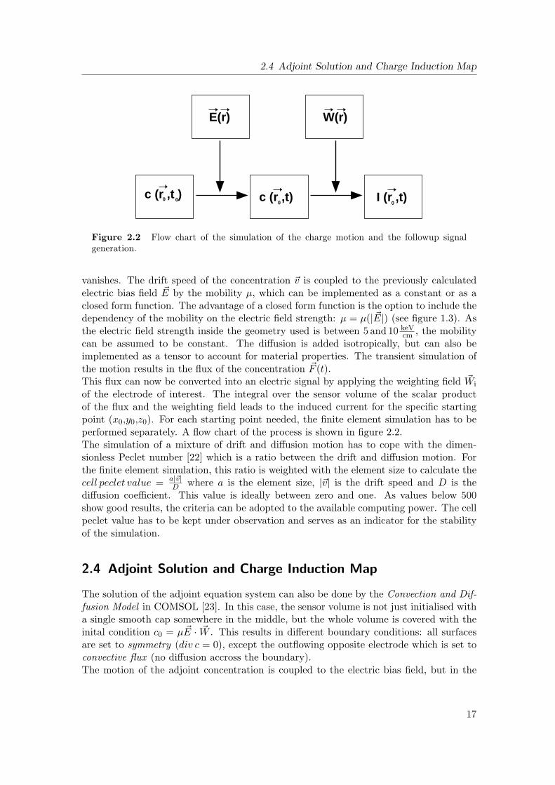
2.3 Charge Motion and Electric Induction
The charge motion can be modelled as a concentration motion within the COMSOLsoftware using the Convection and Diffusion Model [14]. The electric repulsion is neglectedin this approach. The initial charge cloud, i.e. concentration distribution, is modelled bya smooth cap to suppress unphysical diffusion gradients.
c0 =(
1 + cos
(πr
r0
))(r < r0) (2.1)
With this function, the concentration has its maximum in the centre (x0,y0,z0) and withincreasing radial distance r =
√(x− x0)2 + (y − y0)2 + (z − z0)2 the concentration is de-
creasing and slowly reaching zero at the boundaries of the sphere with radius r0.All sensor surfaces are set to zero, i.e. c = 0, so any concentration touching the boundaries
16
2.4 Adjoint Solution and Charge Induction Map
c (r ,t )0 0 c (r ,t)0
E(r) W(r)
0I (r ,t)
Figure 2.2 Flow chart of the simulation of the charge motion and the followup signalgeneration.
vanishes. The drift speed of the concentration ~v is coupled to the previously calculatedelectric bias field ~E by the mobility µ, which can be implemented as a constant or as aclosed form function. The advantage of a closed form function is the option to include thedependency of the mobility on the electric field strength: µ = µ(| ~E|) (see figure 1.3). Asthe electric field strength inside the geometry used is between 5 and 10 keV
cm , the mobilitycan be assumed to be constant. The diffusion is added isotropically, but can also beimplemented as a tensor to account for material properties. The transient simulation ofthe motion results in the flux of the concentration ~F (t).This flux can now be converted into an electric signal by applying the weighting field ~Wi
of the electrode of interest. The integral over the sensor volume of the scalar productof the flux and the weighting field leads to the induced current for the specific startingpoint (x0,y0,z0). For each starting point needed, the finite element simulation has to beperformed separately. A flow chart of the process is shown in figure 2.2.The simulation of a mixture of drift and diffusion motion has to cope with the dimen-sionless Peclet number [22] which is a ratio between the drift and diffusion motion. Forthe finite element simulation, this ratio is weighted with the element size to calculate thecell peclet value = a|~v|
D where a is the element size, |~v| is the drift speed and D is thediffusion coefficient. This value is ideally between zero and one. As values below 500show good results, the criteria can be adopted to the available computing power. The cellpeclet value has to be kept under observation and serves as an indicator for the stabilityof the simulation.
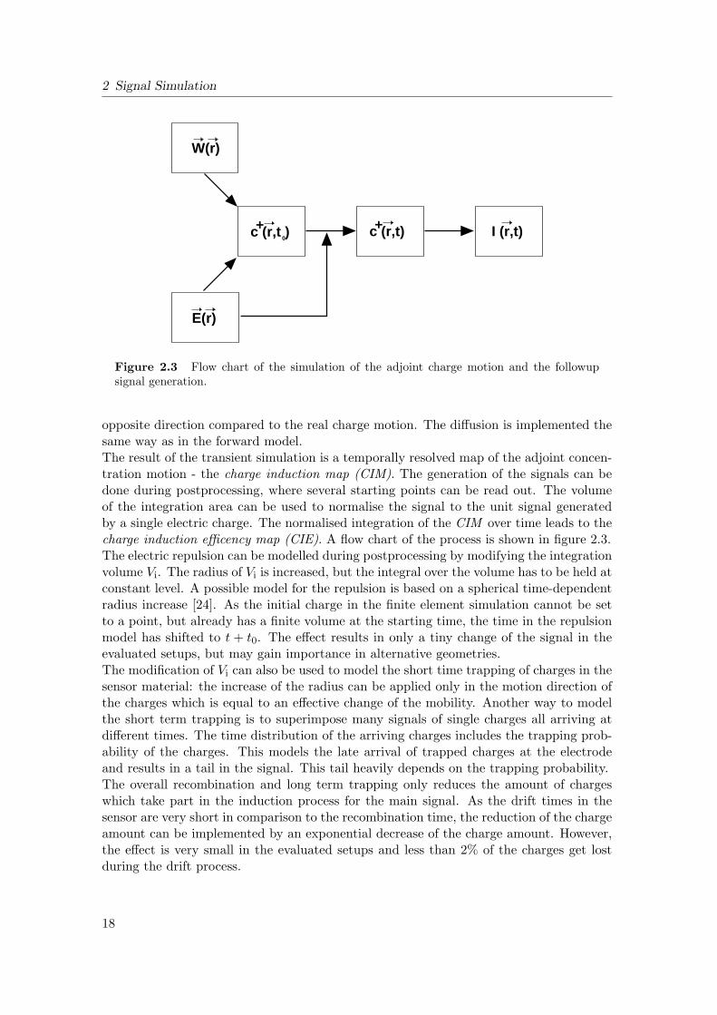
2.4 Adjoint Solution and Charge Induction Map
The solution of the adjoint equation system can also be done by the Convection and Dif-fusion Model in COMSOL [23]. In this case, the sensor volume is not just initialised witha single smooth cap somewhere in the middle, but the whole volume is covered with theinital condition c0 = µ~E · ~W . This results in different boundary conditions: all surfacesare set to symmetry (div c = 0), except the outflowing opposite electrode which is set toconvective flux (no diffusion accross the boundary).The motion of the adjoint concentration is coupled to the electric bias field, but in the
17
2 Signal Simulation
W(r)
E(r)
c (r,t)+ I (r,t)0
c (r,t )+
Figure 2.3 Flow chart of the simulation of the adjoint charge motion and the followupsignal generation.
opposite direction compared to the real charge motion. The diffusion is implemented thesame way as in the forward model.The result of the transient simulation is a temporally resolved map of the adjoint concen-tration motion - the charge induction map (CIM). The generation of the signals can bedone during postprocessing, where several starting points can be read out. The volumeof the integration area can be used to normalise the signal to the unit signal generatedby a single electric charge. The normalised integration of the CIM over time leads to thecharge induction efficency map (CIE). A flow chart of the process is shown in figure 2.3.The electric repulsion can be modelled during postprocessing by modifying the integrationvolume Vi. The radius of Vi is increased, but the integral over the volume has to be held atconstant level. A possible model for the repulsion is based on a spherical time-dependentradius increase [24]. As the initial charge in the finite element simulation cannot be setto a point, but already has a finite volume at the starting time, the time in the repulsionmodel has shifted to t + t0. The effect results in only a tiny change of the signal in theevaluated setups, but may gain importance in alternative geometries.The modification of Vi can also be used to model the short time trapping of charges in thesensor material: the increase of the radius can be applied only in the motion direction ofthe charges which is equal to an effective change of the mobility. Another way to modelthe short term trapping is to superimpose many signals of single charges all arriving atdifferent times. The time distribution of the arriving charges includes the trapping prob-ability of the charges. This models the late arrival of trapped charges at the electrodeand results in a tail in the signal. This tail heavily depends on the trapping probability.The overall recombination and long term trapping only reduces the amount of chargeswhich take part in the induction process for the main signal. As the drift times in thesensor are very short in comparison to the recombination time, the reduction of the chargeamount can be implemented by an exponential decrease of the charge amount. However,the effect is very small in the evaluated setups and less than 2% of the charges get lostduring the drift process.
18

2.4 Adjoint Solution and Charge Induction Map
19

3 Results
The results presented in the following section were all obtained by the finite elementsimulation tool COMSOL as described in the last section. The analysis and postprocessingof the signals was performed with Matlab [25].In the standard setup used for simulation the sensor layer is made of CdTe, which has anintrinsic n-type doping of 2.6 × 10¹¹ 1
cm3 = 0.042 Asm3 (depletion voltage Ud = 600V ). As
the thickness is 1500µm, the applied bias voltage is set to 900 V to achieve overdepletionwith respect to the doping of the material. The pixelated surface is divided in squareareas. The pixel pitch is 220µm and the square electrodes have an edge length of 100µmand are positioned in the centre of the pixel. The corners of the electrodes are truncatedto lower the effects of superelevation in the electric field. The collected charges are theelectrons, as the velocity of the holes is a factor of ten smaller than for the electrons andtherefore the hole signals have no application for fast detection. These values are closeto a prototype chip based on the Medipix which is used in the laboratory at the ECAP(Erlangen Centre for Astroparticle Physics) for imaging purposes and have therefore beenused in the simulation to improve the understanding of the system behaviour.
3.1 Electric Fields
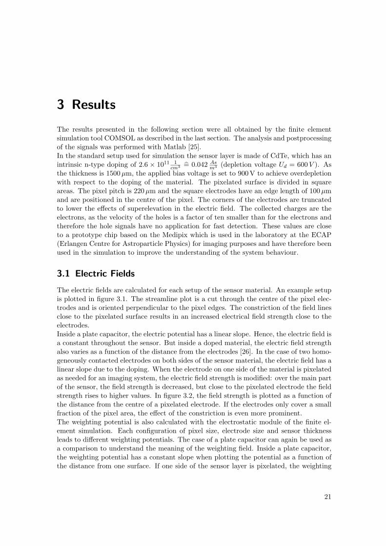
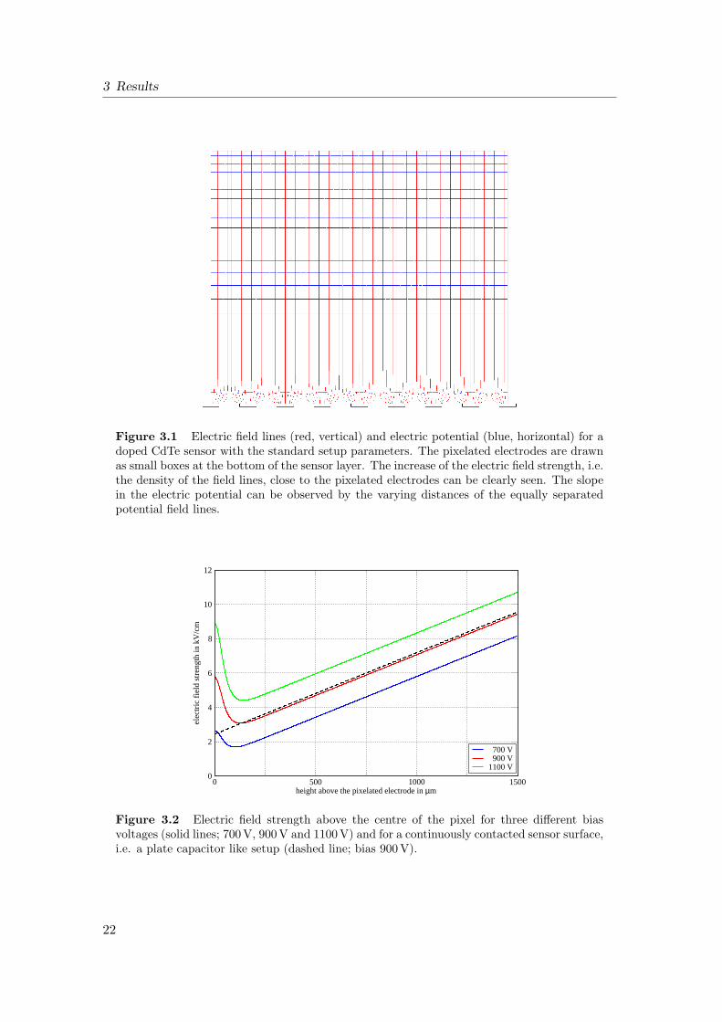
The electric fields are calculated for each setup of the sensor material. An example setupis plotted in figure 3.1. The streamline plot is a cut through the centre of the pixel elec-trodes and is oriented perpendicular to the pixel edges. The constriction of the field linesclose to the pixelated surface results in an increased electrical field strength close to theelectrodes.Inside a plate capacitor, the electric potential has a linear slope. Hence, the electric field isa constant throughout the sensor. But inside a doped material, the electric field strengthalso varies as a function of the distance from the electrodes [26]. In the case of two homo-geneously contacted electrodes on both sides of the sensor material, the electric field has alinear slope due to the doping. When the electrode on one side of the material is pixelatedas needed for an imaging system, the electric field strength is modified: over the main partof the sensor, the field strength is decreased, but close to the pixelated electrode the fieldstrength rises to higher values. In figure 3.2, the field strength is plotted as a function ofthe distance from the centre of a pixelated electrode. If the electrodes only cover a smallfraction of the pixel area, the effect of the constriction is even more prominent.The weighting potential is also calculated with the electrostatic module of the finite el-ement simulation. Each configuration of pixel size, electrode size and sensor thicknessleads to different weighting potentials. The case of a plate capacitor can again be used asa comparison to understand the meaning of the weighting field. Inside a plate capacitor,the weighting potential has a constant slope when plotting the potential as a function ofthe distance from one surface. If one side of the sensor layer is pixelated, the weighting
21
3 Results
Figure 3.1 Electric field lines (red, vertical) and electric potential (blue, horizontal) for adoped CdTe sensor with the standard setup parameters. The pixelated electrodes are drawnas small boxes at the bottom of the sensor layer. The increase of the electric field strength, i.e.the density of the field lines, close to the pixelated electrodes can be clearly seen. The slopein the electric potential can be observed by the varying distances of the equally separatedpotential field lines.
0 500 1000 1500height above the pixelated electrode in µm
0
2
4
6
8
10
12
elec
tric
fie
ld s
tren
gth
in k
V/c
m
700 V 900 V1100 V
Figure 3.2 Electric field strength above the centre of the pixel for three different biasvoltages (solid lines; 700 V, 900 V and 1100 V) and for a continuously contacted sensor surface,i.e. a plate capacitor like setup (dashed line; bias 900 V).
22
3.1 Electric Fields
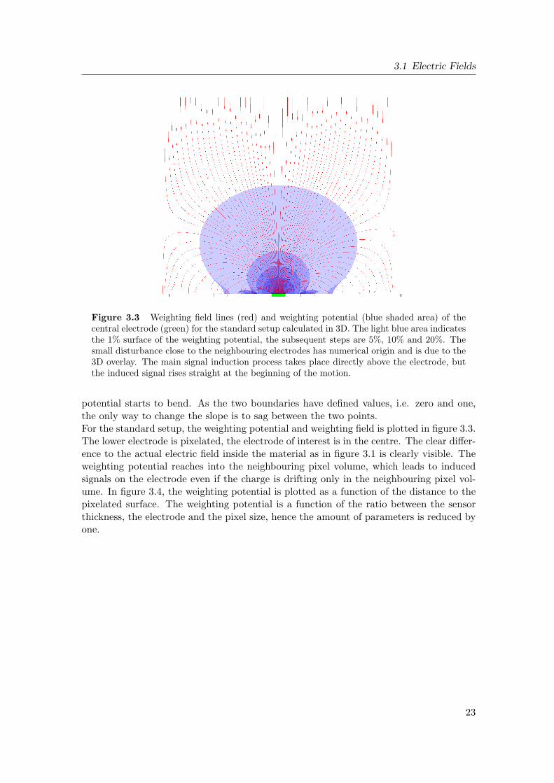
Figure 3.3 Weighting field lines (red) and weighting potential (blue shaded area) of thecentral electrode (green) for the standard setup calculated in 3D. The light blue area indicatesthe 1% surface of the weighting potential, the subsequent steps are 5%, 10% and 20%. Thesmall disturbance close to the neighbouring electrodes has numerical origin and is due to the3D overlay. The main signal induction process takes place directly above the electrode, butthe induced signal rises straight at the beginning of the motion.
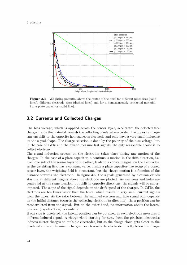
potential starts to bend. As the two boundaries have defined values, i.e. zero and one,the only way to change the slope is to sag between the two points.For the standard setup, the weighting potential and weighting field is plotted in figure 3.3.The lower electrode is pixelated, the electrode of interest is in the centre. The clear differ-ence to the actual electric field inside the material as in figure 3.1 is clearly visible. Theweighting potential reaches into the neighbouring pixel volume, which leads to inducedsignals on the electrode even if the charge is drifting only in the neighbouring pixel vol-ume. In figure 3.4, the weighting potential is plotted as a function of the distance to thepixelated surface. The weighting potential is a function of the ratio between the sensorthickness, the electrode and the pixel size, hence the amount of parameters is reduced byone.
23
3 Results
0 500 1000 1500height above the pixelated electrode in µm
0
0.2
0.4
0.6
0.8
1plate capacitorp: 330 µm e: 150 µmp: 220 µm e: 200 µmp: 220 µm e: 150 µmp: 220 µm e: 100 µmp: 220 µm e: 50 µmp: 110 µm e: 50 µm
Figure 3.4 Weighting potential above the centre of the pixel for different pixel sizes (solidlines), different electrode sizes (dashed lines) and for a homogeneously contacted material,i.e. a plate capacitor (solid line).
3.2 Currents and Collected Charges
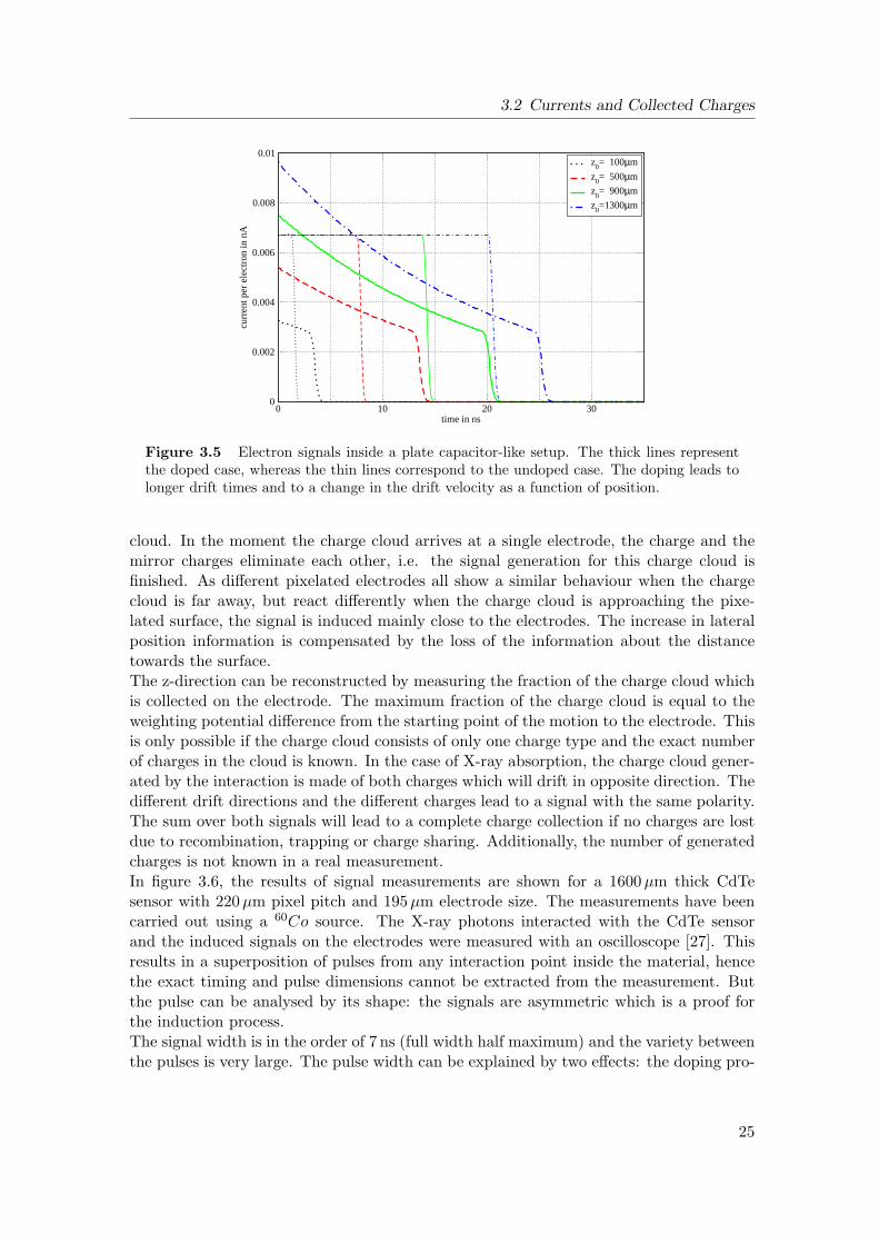
The bias voltage, which is applied across the sensor layer, accelerates the selected freecharges inside the material towards the collecting pixelated electrode. The opposite chargecarriers drift to the opposite homogeneous electrode and only have a very small influenceon the signal shape. The charge selection is done by the polarity of the bias voltage, butin the case of CdTe and the aim to measure fast signals, the only reasonable choice is tocollect electrons.The signal induction process on the electrodes takes place during any motion of thecharges. In the case of a plate capacitor, a continuous motion in the drift direction, i.e.from one side of the sensor layer to the other, leads to a constant signal on the electrodes,as the weighting field has a constant value. Inside a plate capacitor-like setup of a dopedsensor layer, the weighting field is a constant, but the charge motion is a function of thedistance towards the electrode. In figure 3.5, the signals generated by electron cloudsstarting at different heights above the electrode are plotted. As electrons and holes aregenerated at the same location, but drift in opposite directions, the signals will be super-imposed. The slope of the signal depends on the drift speed of the charges. In CdTe, theelectrons are ten times faster then the holes, which results in very small current signalsfrom the holes. As the ratio between the summed electron and hole signal only dependson the initial distance towards the collecting electrode (z-direction), the z-position can bereconstructed from the signal. But on the other hand, no information about the lateralposition (x-y-direction) is available.If one side is pixelated, the lateral position can be obtained as each electrode measures adifferent induced signal. A charge cloud starting far away from the pixelated electrodesinduces mirror charges on multiple electrodes, but as the charge cloud gets closer to thepixelated surface, the mirror charges move towards the electrode directly below the charge
24
3.2 Currents and Collected Charges
0 10 20 30time in ns
0
0.002
0.004
0.006
0.008
0.01
curr
ent p
er e
lect
ron
in n
A
z0= 100µm
z0= 500µm
z0= 900µm
z0=1300µm
Figure 3.5 Electron signals inside a plate capacitor-like setup. The thick lines representthe doped case, whereas the thin lines correspond to the undoped case. The doping leads tolonger drift times and to a change in the drift velocity as a function of position.
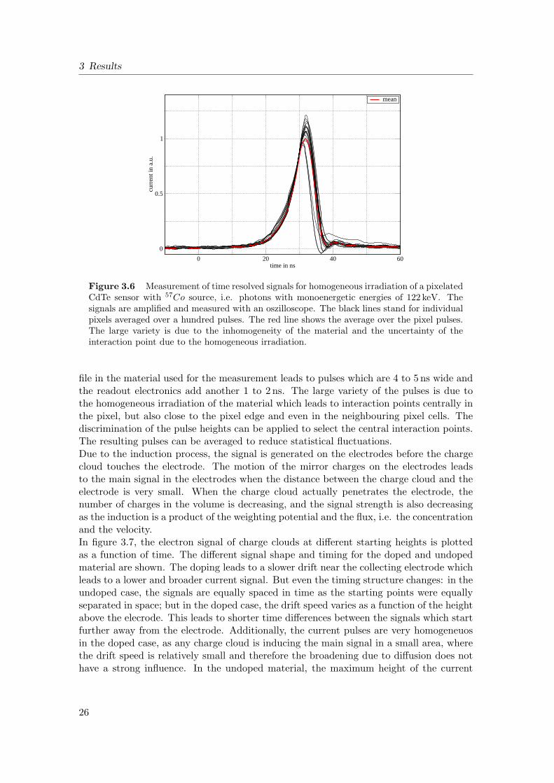
cloud. In the moment the charge cloud arrives at a single electrode, the charge and themirror charges eliminate each other, i.e. the signal generation for this charge cloud isfinished. As different pixelated electrodes all show a similar behaviour when the chargecloud is far away, but react differently when the charge cloud is approaching the pixe-lated surface, the signal is induced mainly close to the electrodes. The increase in lateralposition information is compensated by the loss of the information about the distancetowards the surface.The z-direction can be reconstructed by measuring the fraction of the charge cloud whichis collected on the electrode. The maximum fraction of the charge cloud is equal to theweighting potential difference from the starting point of the motion to the electrode. Thisis only possible if the charge cloud consists of only one charge type and the exact numberof charges in the cloud is known. In the case of X-ray absorption, the charge cloud gener-ated by the interaction is made of both charges which will drift in opposite direction. Thedifferent drift directions and the different charges lead to a signal with the same polarity.The sum over both signals will lead to a complete charge collection if no charges are lostdue to recombination, trapping or charge sharing. Additionally, the number of generatedcharges is not known in a real measurement.In figure 3.6, the results of signal measurements are shown for a 1600µm thick CdTesensor with 220µm pixel pitch and 195µm electrode size. The measurements have beencarried out using a 60Co source. The X-ray photons interacted with the CdTe sensorand the induced signals on the electrodes were measured with an oscilloscope [27]. Thisresults in a superposition of pulses from any interaction point inside the material, hencethe exact timing and pulse dimensions cannot be extracted from the measurement. Butthe pulse can be analysed by its shape: the signals are asymmetric which is a proof forthe induction process.The signal width is in the order of 7 ns (full width half maximum) and the variety betweenthe pulses is very large. The pulse width can be explained by two effects: the doping pro-
25
3 Results
0 20 40 60time in ns
0
0.5
1
curr
ent i
n a.
u.
mean
Figure 3.6 Measurement of time resolved signals for homogeneous irradiation of a pixelatedCdTe sensor with 57Co source, i.e. photons with monoenergetic energies of 122 keV. Thesignals are amplified and measured with an oszilloscope. The black lines stand for individualpixels averaged over a hundred pulses. The red line shows the average over the pixel pulses.The large variety is due to the inhomogeneity of the material and the uncertainty of theinteraction point due to the homogeneous irradiation.
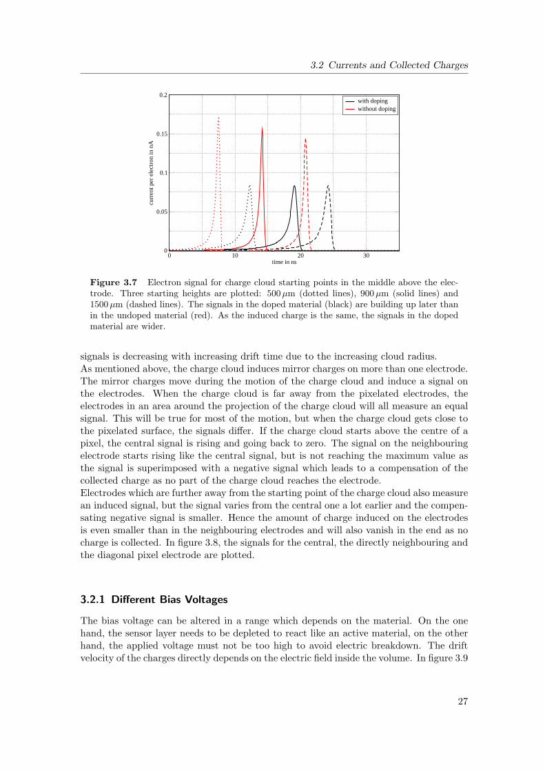
file in the material used for the measurement leads to pulses which are 4 to 5 ns wide andthe readout electronics add another 1 to 2 ns. The large variety of the pulses is due tothe homogeneous irradiation of the material which leads to interaction points centrally inthe pixel, but also close to the pixel edge and even in the neighbouring pixel cells. Thediscrimination of the pulse heights can be applied to select the central interaction points.The resulting pulses can be averaged to reduce statistical fluctuations.Due to the induction process, the signal is generated on the electrodes before the chargecloud touches the electrode. The motion of the mirror charges on the electrodes leadsto the main signal in the electrodes when the distance between the charge cloud and theelectrode is very small. When the charge cloud actually penetrates the electrode, thenumber of charges in the volume is decreasing, and the signal strength is also decreasingas the induction is a product of the weighting potential and the flux, i.e. the concentrationand the velocity.In figure 3.7, the electron signal of charge clouds at different starting heights is plottedas a function of time. The different signal shape and timing for the doped and undopedmaterial are shown. The doping leads to a slower drift near the collecting electrode whichleads to a lower and broader current signal. But even the timing structure changes: in theundoped case, the signals are equally spaced in time as the starting points were equallyseparated in space; but in the doped case, the drift speed varies as a function of the heightabove the elecrode. This leads to shorter time differences between the signals which startfurther away from the electrode. Additionally, the current pulses are very homogeneuosin the doped case, as any charge cloud is inducing the main signal in a small area, wherethe drift speed is relatively small and therefore the broadening due to diffusion does nothave a strong influence. In the undoped material, the maximum height of the current
26
3.2 Currents and Collected Charges
0 10 20 30time in ns
0
0.05
0.1
0.15
0.2
curr
ent p
er e
lect
ron
in n
A
with dopingwithout doping
Figure 3.7 Electron signal for charge cloud starting points in the middle above the elec-trode. Three starting heights are plotted: 500µm (dotted lines), 900µm (solid lines) and1500µm (dashed lines). The signals in the doped material (black) are building up later thanin the undoped material (red). As the induced charge is the same, the signals in the dopedmaterial are wider.
signals is decreasing with increasing drift time due to the increasing cloud radius.As mentioned above, the charge cloud induces mirror charges on more than one electrode.The mirror charges move during the motion of the charge cloud and induce a signal onthe electrodes. When the charge cloud is far away from the pixelated electrodes, theelectrodes in an area around the projection of the charge cloud will all measure an equalsignal. This will be true for most of the motion, but when the charge cloud gets close tothe pixelated surface, the signals differ. If the charge cloud starts above the centre of apixel, the central signal is rising and going back to zero. The signal on the neighbouringelectrode starts rising like the central signal, but is not reaching the maximum value asthe signal is superimposed with a negative signal which leads to a compensation of thecollected charge as no part of the charge cloud reaches the electrode.Electrodes which are further away from the starting point of the charge cloud also measurean induced signal, but the signal varies from the central one a lot earlier and the compen-sating negative signal is smaller. Hence the amount of charge induced on the electrodesis even smaller than in the neighbouring electrodes and will also vanish in the end as nocharge is collected. In figure 3.8, the signals for the central, the directly neighbouring andthe diagonal pixel electrode are plotted.
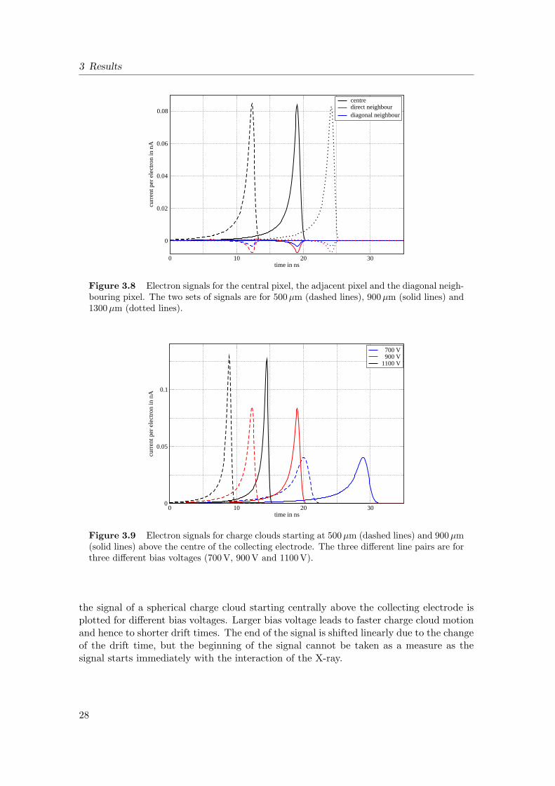
3.2.1 Different Bias Voltages
The bias voltage can be altered in a range which depends on the material. On the onehand, the sensor layer needs to be depleted to react like an active material, on the otherhand, the applied voltage must not be too high to avoid electric breakdown. The driftvelocity of the charges directly depends on the electric field inside the volume. In figure 3.9
27
3 Results
0 10 20 30time in ns
0
0.02
0.04
0.06
0.08
curr
ent p
er e
lect
ron
in n
A
centredirect neighbourdiagonal neighbour
Figure 3.8 Electron signals for the central pixel, the adjacent pixel and the diagonal neigh-bouring pixel. The two sets of signals are for 500µm (dashed lines), 900µm (solid lines) and1300µm (dotted lines).
0 10 20 30time in ns
0
0.05
0.1
curr
ent p
er e
lect
ron
in n
A
700 V 900 V1100 V
Figure 3.9 Electron signals for charge clouds starting at 500µm (dashed lines) and 900µm(solid lines) above the centre of the collecting electrode. The three different line pairs are forthree different bias voltages (700 V, 900 V and 1100 V).
the signal of a spherical charge cloud starting centrally above the collecting electrode isplotted for different bias voltages. Larger bias voltage leads to faster charge cloud motionand hence to shorter drift times. The end of the signal is shifted linearly due to the changeof the drift time, but the beginning of the signal cannot be taken as a measure as thesignal starts immediately with the interaction of the X-ray.
28
3.2 Currents and Collected Charges
0 10 20 30time in ns
0
0.5
1
1.5
2
2.5
3
curr
ent i
n µA
1*104
electrons
2*104
electrons
3*104
electrons
Figure 3.10 Electron signals for charge clouds starting at 500µm (dashed lines) and 900µm(solid lines) above the centre of the collecting electrode. The three different lines are for threedifferent integrated charge amounts.
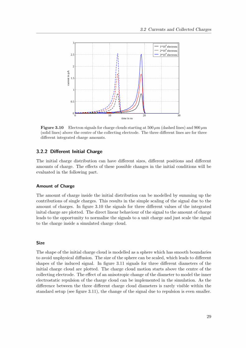
3.2.2 Different Initial Charge
The initial charge distribution can have different sizes, different positions and differentamounts of charge. The effects of these possible changes in the initial conditions will beevaluated in the following part.
Amount of Charge
The amount of charge inside the initial distribution can be modelled by summing up thecontributions of single charges. This results in the simple scaling of the signal due to theamount of charges. In figure 3.10 the signals for three different values of the integratedinital charge are plotted. The direct linear behaviour of the signal to the amount of chargeleads to the opportunity to normalise the signals to a unit charge and just scale the signalto the charge inside a simulated charge cloud.
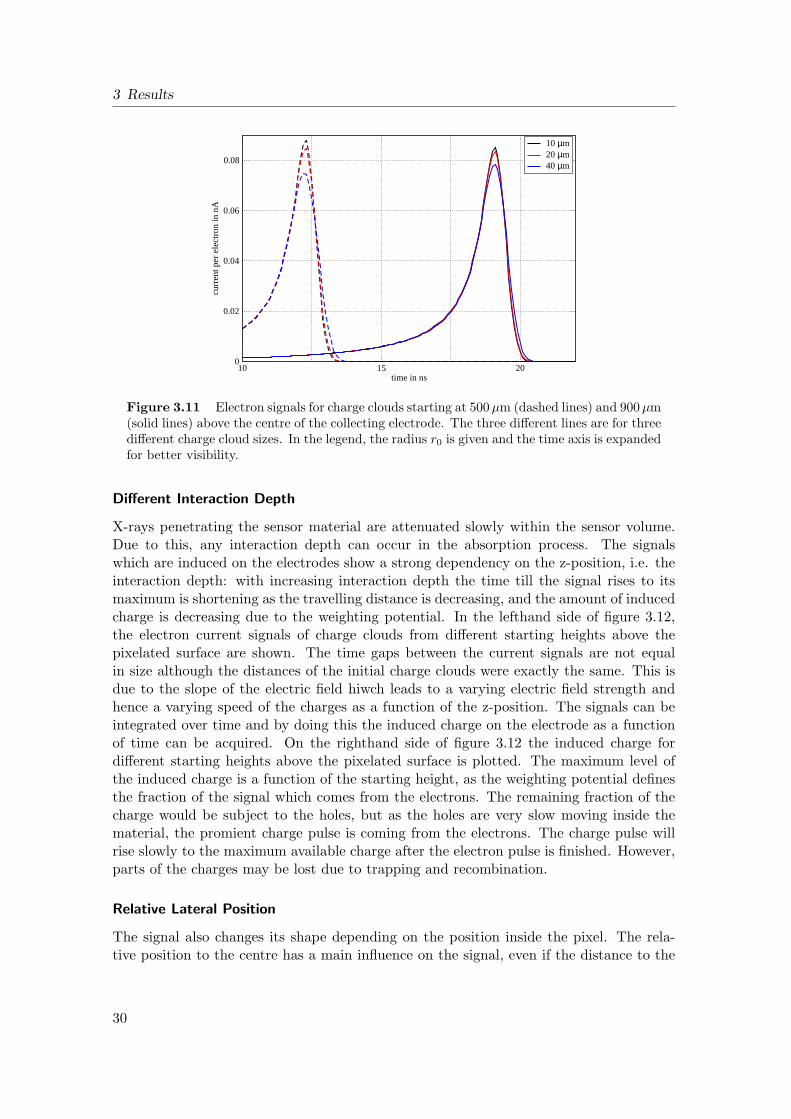
Size
The shape of the initial charge cloud is modelled as a sphere which has smooth boundariesto avoid unphysical diffusion. The size of the sphere can be scaled, which leads to differentshapes of the induced signal. In figure 3.11 signals for three different diameters of theinitial charge cloud are plotted. The charge cloud motion starts above the centre of thecollecting electrode. The effect of an anisotropic change of the diameter to model the innerelectrostatic repulsion of the charge cloud can be implemented in the simulation. As thedifference between the three different charge cloud diameters is rarely visible within thestandard setup (see figure 3.11), the change of the signal due to repulsion is even smaller.
29
3 Results
10 15 20time in ns
0
0.02
0.04
0.06
0.08
curr
ent p
er e
lect
ron
in n
A
10 µm20 µm40 µm
Figure 3.11 Electron signals for charge clouds starting at 500µm (dashed lines) and 900µm(solid lines) above the centre of the collecting electrode. The three different lines are for threedifferent charge cloud sizes. In the legend, the radius r0 is given and the time axis is expandedfor better visibility.
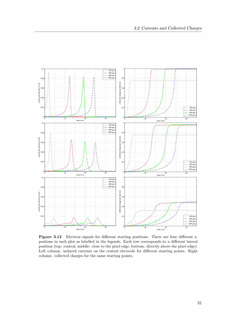
Different Interaction Depth
X-rays penetrating the sensor material are attenuated slowly within the sensor volume.Due to this, any interaction depth can occur in the absorption process. The signalswhich are induced on the electrodes show a strong dependency on the z-position, i.e. theinteraction depth: with increasing interaction depth the time till the signal rises to itsmaximum is shortening as the travelling distance is decreasing, and the amount of inducedcharge is decreasing due to the weighting potential. In the lefthand side of figure 3.12,the electron current signals of charge clouds from different starting heights above thepixelated surface are shown. The time gaps between the current signals are not equalin size although the distances of the initial charge clouds were exactly the same. This isdue to the slope of the electric field hiwch leads to a varying electric field strength andhence a varying speed of the charges as a function of the z-position. The signals can beintegrated over time and by doing this the induced charge on the electrode as a functionof time can be acquired. On the righthand side of figure 3.12 the induced charge fordifferent starting heights above the pixelated surface is plotted. The maximum level ofthe induced charge is a function of the starting height, as the weighting potential definesthe fraction of the signal which comes from the electrons. The remaining fraction of thecharge would be subject to the holes, but as the holes are very slow moving inside thematerial, the promient charge pulse is coming from the electrons. The charge pulse willrise slowly to the maximum available charge after the electron pulse is finished. However,parts of the charges may be lost due to trapping and recombination.
Relative Lateral Position
The signal also changes its shape depending on the position inside the pixel. The rela-tive position to the centre has a main influence on the signal, even if the distance to the
30
3.2 Currents and Collected Charges
0 10 20 30time in ns
0
0.02
0.04
0.06
0.08
0.1
curr
ent p
er e
lect
ron
in n
A
100 µm 500 µm 900 µm1300 µm
0 10 20 30time in ns
0
0.2
0.4
0.6
0.8
1
colle
cted
cha
rge
per
elec
tron
100 µm 500 µm 900 µm1300 µm
0 10 20 30time in ns
0
0.02
0.04
0.06
0.08
0.1
curr
ent p
er e
lect
ron
in n
A
100 µm 500 µm 900 µm1300 µm
0 10 20 30time in ns
0
0.2
0.4
0.6
0.8
1
colle
cted
cha
rge
per
elec
tron
100 µm 500 µm 900 µm1300 µm
0 10 20 30time in ns
0
0.02
0.04
0.06
0.08
0.1
curr
ent p
er e
lect
ron
in n
A
100 µm 500 µm 900 µm1300 µm
0 10 20 30time in ns
0
0.2
0.4
0.6
0.8
1
colle
cted
cha
rge
per
elec
tron
100 µm 500 µm 900 µm1300 µm
Figure 3.12 Electron signals for different starting positions. There are four different z-positons in each plot as labelled in the legends. Each row corresponds to a different lateralposition (top: central, middle: close to the pixel edge, bottom: directly above the pixel edge).Left column: induced currents on the central electrode for different starting points. Rightcolumn: collected charges for the same starting points.
31
3 Results
pixelated surface is the same. Charge clouds which start close to the edges of the pixeldeposit parts of the charge in the neighbouring pixel, which is then missing in the centralsignal. But even if all the charge is collected inside the central pixel, the shape of thesignal can vary due to the subpixel position. As the charges may have to travel a longerdistance to the electrode, the signal is getting broader.In figure 3.12 the effect of different subpixelpositions is shown. Each row corresponds to aspecific position. In the top row, the charge cloud starts at positions on the central axis ofthe pixel and the z-position is set as labelled in the plot. For the bottom row, the chargecloud was set directly above the pixel edge, i.e. the x-position is 110µm. In the middle,the starting points vary along a line which is close to the pixel edge, i.e. y-position is setto the origin, the x-position is set to 80µm (which is in the area of the pixel where noelectrode is straight beneath).
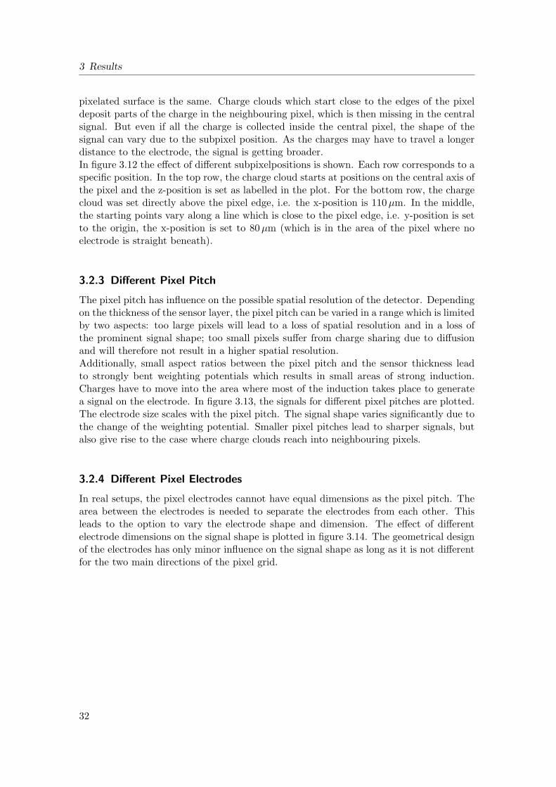
3.2.3 Different Pixel Pitch
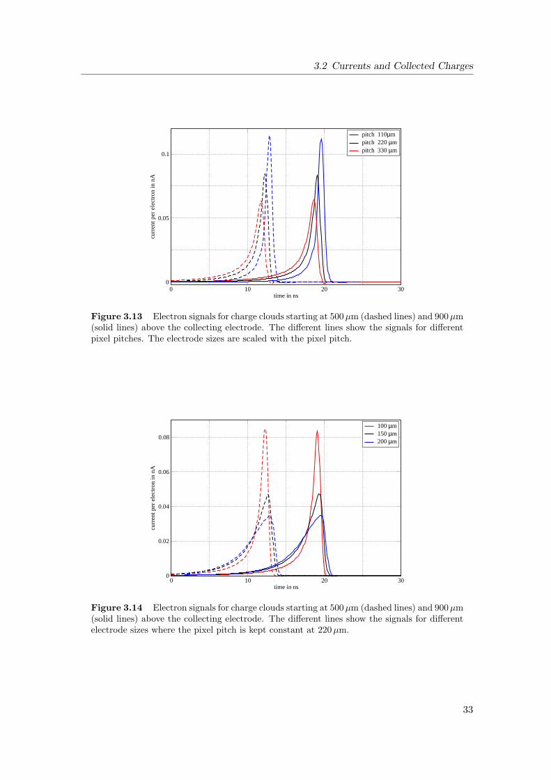
The pixel pitch has influence on the possible spatial resolution of the detector. Dependingon the thickness of the sensor layer, the pixel pitch can be varied in a range which is limitedby two aspects: too large pixels will lead to a loss of spatial resolution and in a loss ofthe prominent signal shape; too small pixels suffer from charge sharing due to diffusionand will therefore not result in a higher spatial resolution.Additionally, small aspect ratios between the pixel pitch and the sensor thickness leadto strongly bent weighting potentials which results in small areas of strong induction.Charges have to move into the area where most of the induction takes place to generatea signal on the electrode. In figure 3.13, the signals for different pixel pitches are plotted.The electrode size scales with the pixel pitch. The signal shape varies significantly due tothe change of the weighting potential. Smaller pixel pitches lead to sharper signals, butalso give rise to the case where charge clouds reach into neighbouring pixels.
3.2.4 Different Pixel Electrodes
In real setups, the pixel electrodes cannot have equal dimensions as the pixel pitch. Thearea between the electrodes is needed to separate the electrodes from each other. Thisleads to the option to vary the electrode shape and dimension. The effect of differentelectrode dimensions on the signal shape is plotted in figure 3.14. The geometrical designof the electrodes has only minor influence on the signal shape as long as it is not differentfor the two main directions of the pixel grid.
32
3.2 Currents and Collected Charges
0 10 20 30time in ns
0
0.05
0.1cu
rren
t per
ele
ctro
n in
nA
pitch 110µmpitch 220 µmpitch 330 µm
Figure 3.13 Electron signals for charge clouds starting at 500µm (dashed lines) and 900µm(solid lines) above the collecting electrode. The different lines show the signals for differentpixel pitches. The electrode sizes are scaled with the pixel pitch.
0 10 20 30time in ns
0
0.02
0.04
0.06
0.08
curr
ent p
er e
lect
ron
in n
A
100 µm150 µm200 µm
Figure 3.14 Electron signals for charge clouds starting at 500µm (dashed lines) and 900µm(solid lines) above the collecting electrode. The different lines show the signals for differentelectrode sizes where the pixel pitch is kept constant at 220µm.
33
3 Results
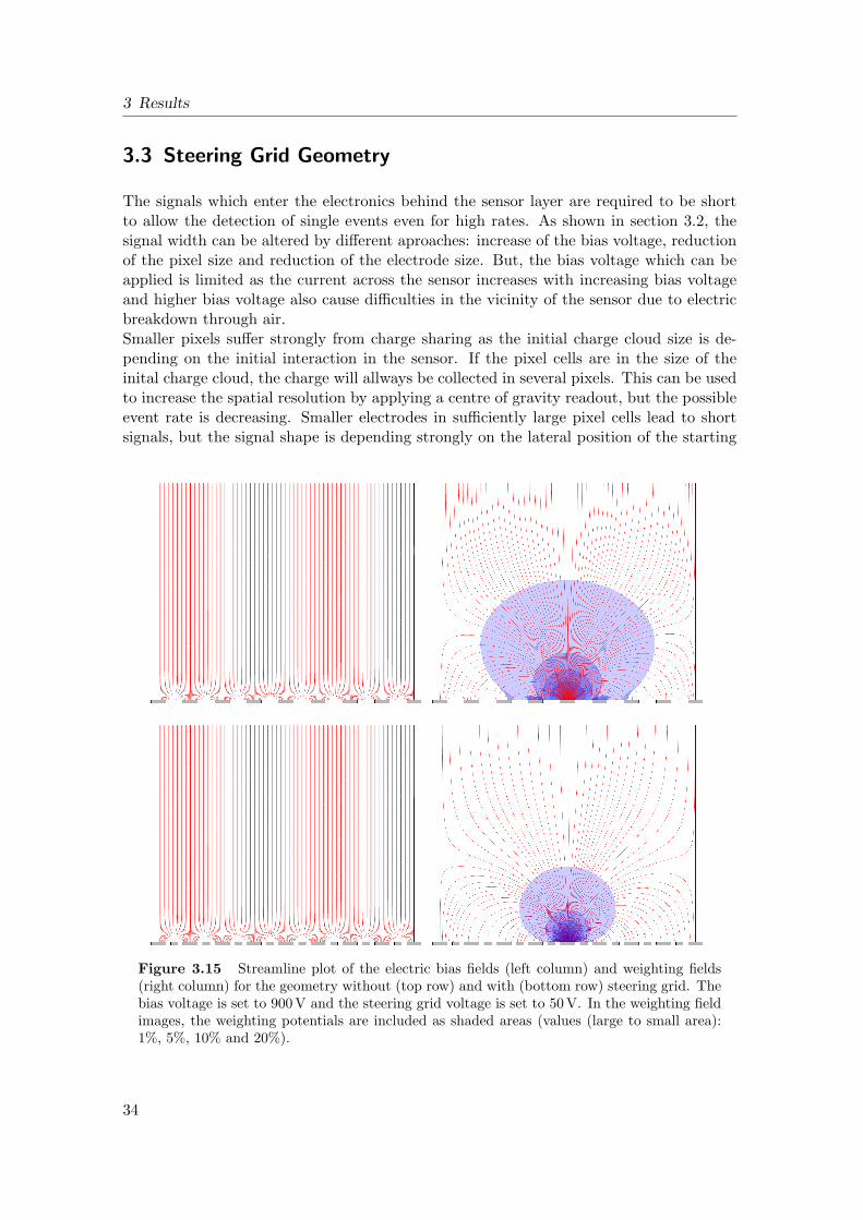
3.3 Steering Grid Geometry
The signals which enter the electronics behind the sensor layer are required to be shortto allow the detection of single events even for high rates. As shown in section 3.2, thesignal width can be altered by different aproaches: increase of the bias voltage, reductionof the pixel size and reduction of the electrode size. But, the bias voltage which can beapplied is limited as the current across the sensor increases with increasing bias voltageand higher bias voltage also cause difficulties in the vicinity of the sensor due to electricbreakdown through air.Smaller pixels suffer strongly from charge sharing as the initial charge cloud size is de-pending on the initial interaction in the sensor. If the pixel cells are in the size of theinital charge cloud, the charge will allways be collected in several pixels. This can be usedto increase the spatial resolution by applying a centre of gravity readout, but the possibleevent rate is decreasing. Smaller electrodes in sufficiently large pixel cells lead to shortsignals, but the signal shape is depending strongly on the lateral position of the starting
Figure 3.15 Streamline plot of the electric bias fields (left column) and weighting fields(right column) for the geometry without (top row) and with (bottom row) steering grid. Thebias voltage is set to 900 V and the steering grid voltage is set to 50 V. In the weighting fieldimages, the weighting potentials are included as shaded areas (values (large to small area):1%, 5%, 10% and 20%).
34
3.3 Steering Grid Geometry
0 10 20 30time in ns
0
0.5
1
curr
ent i
n a.
u.
with steering gridwithout steering grid
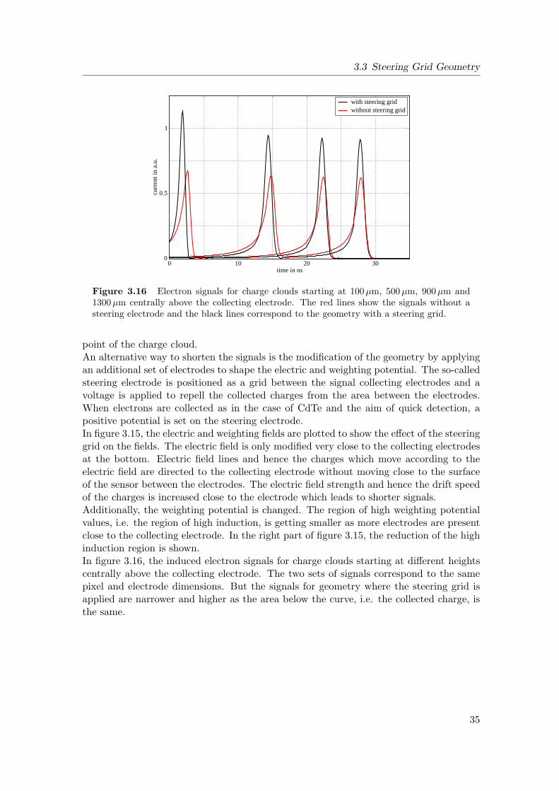
Figure 3.16 Electron signals for charge clouds starting at 100µm, 500µm, 900µm and1300µm centrally above the collecting electrode. The red lines show the signals without asteering electrode and the black lines correspond to the geometry with a steering grid.
point of the charge cloud.An alternative way to shorten the signals is the modification of the geometry by applyingan additional set of electrodes to shape the electric and weighting potential. The so-calledsteering electrode is positioned as a grid between the signal collecting electrodes and avoltage is applied to repell the collected charges from the area between the electrodes.When electrons are collected as in the case of CdTe and the aim of quick detection, apositive potential is set on the steering electrode.In figure 3.15, the electric and weighting fields are plotted to show the effect of the steeringgrid on the fields. The electric field is only modified very close to the collecting electrodesat the bottom. Electric field lines and hence the charges which move according to theelectric field are directed to the collecting electrode without moving close to the surfaceof the sensor between the electrodes. The electric field strength and hence the drift speedof the charges is increased close to the electrode which leads to shorter signals.Additionally, the weighting potential is changed. The region of high weighting potentialvalues, i.e. the region of high induction, is getting smaller as more electrodes are presentclose to the collecting electrode. In the right part of figure 3.15, the reduction of the highinduction region is shown.In figure 3.16, the induced electron signals for charge clouds starting at different heightscentrally above the collecting electrode. The two sets of signals correspond to the samepixel and electrode dimensions. But the signals for geometry where the steering grid isapplied are narrower and higher as the area below the curve, i.e. the collected charge, isthe same.
35

4 Summary and Discussion of Part I
The calculation of the electric potential and its gradient, i.e. the electric field, can beperformed in a rather direct way as the shape of the potential is repeating in each singlepixel cell. This repetition leads to ideal symmetry conditions which dictate the bound-ary conditions which have to be applied. The doping of the material is implemented asa space charge density. The density can be extracted from electric field measurements.This leads to the option to implement not only homogeneous doping, but also spaciallyvarying doping profiles. In combination, the doping and the clear symmetry lead to verygood results of the electric field calculation, which is shown in figures 3.1 and 3.2.
The weighting potential calculation suffers from the fundamental restriction of the simu-lation volume while the potential is extending to infinity. However, the systematic errorwhich results from the finite size of the simulation volume can be neglected if the simula-tion takes a sufficient large number of neighbouring electrodes into account. The changeof the potential in the central pixel cell which is observed in the signal induction process isdiminishing when more neighbouring electrodes are added and so the weighting potentialis almost reaching its final shape. The simulation takes four neighbouring pixel cells inall four directions into account which results in a 9x9 pixel simulation area. This leads toa good agreement with the final shape within a reasonable memory and computing timeconsumption.
The currents which are induced on the electrodes originate in the motion of the mir-ror charges. The simple case of a plate capacitor setup can be observed for clarity. Anelectron cloud starting in the middle of the sensor and moving to the positive electrodeinduces a constant signal during its motion as the electric and the weighting potentialhave the same shape. As electrons and holes are generated in pairs by the interactionof X-rays with the sensor, the holes will drift in the opposite direction. The drift willbe slower due to a smaller mobility of the holes, but the induced signal will have thesame sign, as the motion direction and the charge sign are both changed. In figure 3.5,only the electron signal is plotted. The hole signal would be added to the electron signalwhich leads to an additional step in the graph. The timing of the two steps depends onthe z-position of the starting position, but the relative signal height is due to the ratiobetween the mobilities of electrons and holes.Doping of the sensor material leads to an inhomogeneous electric field strength and hencean inhomogeneous drift velocity. The collected charge on the electrode depends on thez-position of the starting point, but as the current is the product of the the charge velocityand the weighting field, the signal shape will not be a constant, but tilted as shown infigure 3.5.If the collecting electrode is pixelated, the shape of the signal changes. The inductionprocess is not independant of the z-position in the sensor, but has a maximum close to
37
4 Summary and Discussion of Part I
the collecting electrode. The weighting field maximum close to the collecting electrodeleads to the main signal induction close to the electrode. The motion of the charge cloudat larger distances has only minor influence on the signal. Therefore, the hole motionloses impact on the generated signal. For this reason, the hole motion is neglected in thefollowing simulation.
As in the plate capacitor geometry, the doping of the material has a strong influenceon the signal. In the evaluated geometry, n-type material leads to slower motion on thecharges close to the collecting electrode. Thus, the signal is building up later and is get-ting wider, as shown in figure 3.7. As the collected charge is the same, the signal heightis decreased. Additionally, the signal height is varying less with the z-position of thestarting point as the diffusion is not affecting the temporal shape of the signal as muchas the slowing down of the drift velocity by the doping.The pulse shape was investigated with respect to different parameters. The bias voltageregulates the electric field strength inside the material. As the drift motion is directly cou-pled to the electric field by the mobility, the pulses change with the bias voltage. Higherbias voltages lead to shorter drift times and to sharper signals which can be observed infigure 3.9. The number of electrons in the charge cloud only results in a higher signal,but the signal shape is not changing.The lateral position inside the pixel cell has some influence on the signal shape (see fig-ure 3.12): starting points at the center of the pixel above the electrode induce a strongand sharp signal as the motion of the charge cloud is direct. If the charge cloud startscloser to the pixel edge, some charge may drift or diffuse in the neighbouring pixel whichleads to a loss of signal in the central pixel. But even starting points where the wholecharge is collected by the central electrode can have smaller and wider signals. If thecharge motion is not perpendicular to the electrode surface but has to drift sideways toarrive at the electrode, the current pulse will be wider due to the elongated drift way closeto the collecting electrode.This drift way elongation depends on the ratio of the pixel pitch and the electrode size.Smaller electrodes cover less of the pixel area and hence more lateral drift is necessaryto reach the electrode. Additionally, the area of strong weighting potential gradients isgetting smaller when the electrodes are decreasing in size (see figure 3.4). Smaller elec-trodes and smaller pixel pitches both lead to sharper signals, but the spatial resolutionof the detector cannot be improved without limit. The main reason is the distribution ofthe signal to more than one electrode (charge sharing). This is obvious for charge cloudswhich are larger than one pixel cell as some of the charge will drift to the neighbouringelectrode. But even when the charge cloud is smaller than the pixel size, a temporal signalwill be induced on the neighbouring electrode.
The simulation offers a good access to the spatial distribution of the induced currentswhich can help to design future detector geometries. The knowledge of the timing struc-ture of the signals allows the optimisation of the geometry as well as the readout electronicsbehind the sensor layer.
38


Part II
Radiation Field of aMedical Linear Accelerator
41


5 Basics of Medical Irradiation
Medical irradiation is a commonly used treatment method for tumour diseases. The basisfor this treatment is the different response of healthy and tumour tissue to exposurewith ionising radiation. Healthy cells can cope with radiation damage of the DNA moreefficiently than tumour cells. This leads to different survival rates of the different tissuesthus to the possibility to injure or destroy tumour cells (i.e. to force the cells to apoptosis)while keeping healthy cells alive.
5.1 Dose Definition
The effect of ionizing radiation on material depends on the type of radiation, the energyand the material itself. Consequently, there are different definitions to characterize theionizing effect. The following list explaines the most commonly used [28]:
1. Kerma (only photons): The Kinetic Energy Released in MAtter takes account of thekinetic energy of all charged particles generated by non-charged particles interactingwith the material. These charged particles deposit energy in further interactionswith the material, but these secondary processes do not contribute to the kerma K:
K =δEkinδm
(5.1)
The unit of kerma isGray(Gy) = Jkg . This measure can only be applied to uncharged
particles like photons. The air kerma is the kerma of photons in air, which can beobtained at standardized conditions with the help of ionisation chambers.
2. Absorbed Energy Dose: The complete energy δEabs deposited in material of massδm by incoming ionizing radiation is described by the absorbed energy dose:
D =δEabsδm
(5.2)
The unit of the absorbed energy dose is Gray(Gy) = Jkg , which is equal to the unit
of kerma. But in this case, the transfer of energy from the charged particles to thematerial is also taken into account.
3. Dose Equivalent : Different types of radiations have different biological effects. Thedose equivalent H equals the absorbed dose, but is weighted with a quality factorfQ (see table 5.1) to take the biological effects into account.
H = fQ ·D = fQ ·δEabsδm
(5.3)
The resulting unit is Sievert(Sv) = [fQ] · Gy = Gy. As the quality factor has nounit, it is the same as for the absorbed energy dose.
43
5 Basics of Medical Irradiation
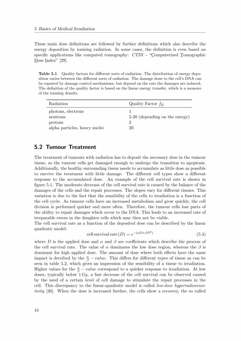
These main dose definitions are followed by further definitions which also describe theenergy deposition by ionising radiation. In some cases, the definition is even based onspecific applications like computed tomography: CTDI - “Computerized TomographicDose Index” [29].
Table 5.1 Quality factors for different sorts of radiation. The distribution of energy depo-sition varies between the different sorts of radiation. The damage done to the cell’s DNA canbe repaired by damage control mechanisms, but depend on the rate the damages are induced.The definition of the quality factor is based on the linear energy transfer, which is a measureof the ionising density.
Radiation Quality Factor fQ
photons, electrons 1neutrons 5-20 (depending on the energy)protons 2alpha particles, heavy nuclei 20
5.2 Tumour Treatment
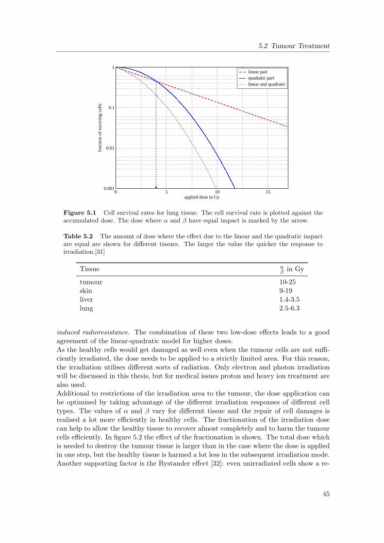
The treatment of tumours with radiation has to deposit the necessary dose in the tumourtissue, so the tumour cells get damaged enough to undergo the transition to apoptosis.Additionally, the healthy surrounding tissue needs to accumulate as little dose as possibleto survive the treatment with little damage. The different cell types show a differentresponse to the accumulated dose. An example of the cell survival rate is shown infigure 5.1. The moderate decrease of the cell survival rate is caused by the balance of thedamages of the cells and the repair processes. The slopes vary for different tissues. Thisvariation is due to the fact that the sensibility of the cells to irradiation is a function ofthe cell cycle. As tumour cells have an increased metabolism and grow quickly, the celldivision is performed quicker and more often. Therefore, the tumour cells lose parts ofthe ability to repair damages which occur to the DNA. This leads to an increased rate ofirreparable errors in the daughter cells which may then not be viable.The cell survival rate as a function of the deposited dose can be described by the linearquadratic model:
cell survival rate (D) = e−(αD+βD2) (5.4)
where D is the applied dose and α and β are coefficients which describe the process ofthe cell survival rate. The value of α dominates the low dose region, whereas the β isdominant for high applied dose. The amount of dose where both effects have the sameimpact is decribed by the α
β − value. This differs for different types of tissue as can beseen in table 5.2, which gives an impression of the sensibility of a tissue to irradiation.Higher values for the α
β − value correspond to a quicker response to irradiation. At lowdoses, typically below 1Gy, a fast decrease of the cell survival can be observed causedby the need of a certain level of cell damage to stimulate the repair processes in thecell. This discrepancy to the linear-quadratic model is called low-dose hyperradiosensi-tivity [30]. When the dose is increased further, the cells show a recovery, the so called
44
5.2 Tumour Treatment
0 5 10 15applied dose in Gy
0.001
0.01
0.1
1
frac
tion
of
suvi
ving
cel
ls
linear partquadratic partlinear and quadratic
Figure 5.1 Cell survival rates for lung tissue. The cell survival rate is plotted against theaccumulated dose. The dose where α and β have equal impact is marked by the arrow.
Table 5.2 The amount of dose where the effect due to the linear and the quadratic impactare equal are shown for different tissues. The larger the value the quicker the response toirradiation.[31]
Tissue αβ in Gy
tumour 10-25skin 9-19liver 1.4-3.5lung 2.5-6.3
induced radioresistance. The combination of these two low-dose effects leads to a goodagreement of the linear-quadratic model for higher doses.As the healthy cells would get damaged as well even when the tumour cells are not suffi-ciently irradiated, the dose needs to be applied to a strictly limited area. For this reason,the irradiation utilises different sorts of radiation. Only electron and photon irradiationwill be discussed in this thesis, but for medical issues proton and heavy ion treatment arealso used.Additional to restrictions of the irradiation area to the tumour, the dose application canbe optimised by taking advantage of the different irradiation responses of different celltypes. The values of α and β vary for different tissue and the repair of cell damages isrealised a lot more efficiently in healthy cells. The fractionation of the irradiation dosecan help to allow the healthy tissue to recover almost completely and to harm the tumourcells efficiently. In figure 5.2 the effect of the fractionation is shown. The total dose whichis needed to destroy the tumour tissue is larger than in the case where the dose is appliedin one step, but the healthy tissue is harmed a lot less in the subsequent irradiation mode.Another supporting factor is the Bystander effect [32]: even unirradiated cells show a re-
45
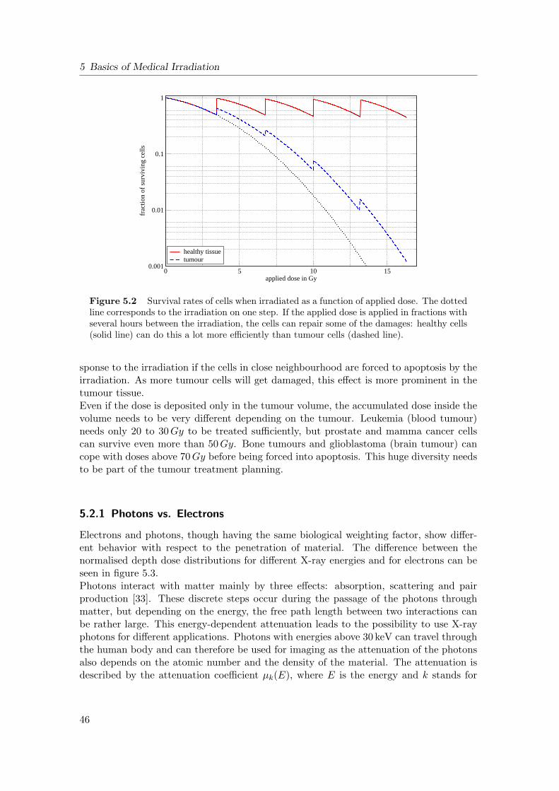
5 Basics of Medical Irradiation
0 5 10 15applied dose in Gy
0.001
0.01
0.1
1
frac
tion
of s
urvi
ving
cel
ls
healthy tissuetumour
Figure 5.2 Survival rates of cells when irradiated as a function of applied dose. The dottedline corresponds to the irradiation on one step. If the applied dose is applied in fractions withseveral hours between the irradiation, the cells can repair some of the damages: healthy cells(solid line) can do this a lot more efficiently than tumour cells (dashed line).
sponse to the irradiation if the cells in close neighbourhood are forced to apoptosis by theirradiation. As more tumour cells will get damaged, this effect is more prominent in thetumour tissue.Even if the dose is deposited only in the tumour volume, the accumulated dose inside thevolume needs to be very different depending on the tumour. Leukemia (blood tumour)needs only 20 to 30Gy to be treated sufficiently, but prostate and mamma cancer cellscan survive even more than 50Gy. Bone tumours and glioblastoma (brain tumour) cancope with doses above 70Gy before being forced into apoptosis. This huge diversity needsto be part of the tumour treatment planning.
5.2.1 Photons vs. Electrons
Electrons and photons, though having the same biological weighting factor, show differ-ent behavior with respect to the penetration of material. The difference between thenormalised depth dose distributions for different X-ray energies and for electrons can beseen in figure 5.3.Photons interact with matter mainly by three effects: absorption, scattering and pairproduction [33]. These discrete steps occur during the passage of the photons throughmatter, but depending on the energy, the free path length between two interactions canbe rather large. This energy-dependent attenuation leads to the possibility to use X-rayphotons for different applications. Photons with energies above 30 keV can travel throughthe human body and can therefore be used for imaging as the attenuation of the photonsalso depends on the atomic number and the density of the material. The attenuation isdescribed by the attenuation coefficient µk(E), where E is the energy and k stands for
46
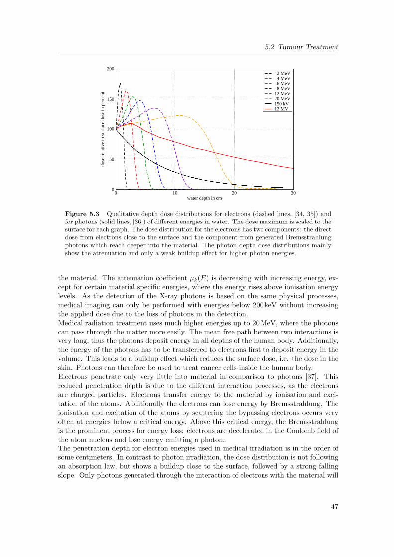
5.2 Tumour Treatment
0 10 20 30water depth in cm
0
50
100
150
200
dose
rel
ativ
e to
sur
face
dos
e in
per
cent
2 MeV 4 MeV 6 MeV 8 MeV12 MeV20 MeV150 kV12 MV
Figure 5.3 Qualitative depth dose distributions for electrons (dashed lines, [34, 35]) andfor photons (solid lines, [36]) of different energies in water. The dose maximum is scaled to thesurface for each graph. The dose distribution for the electrons has two components: the directdose from electrons close to the surface and the component from generated Bremsstrahlungphotons which reach deeper into the material. The photon depth dose distributions mainlyshow the attenuation and only a weak buildup effect for higher photon energies.
the material. The attenuation coefficient µk(E) is decreasing with increasing energy, ex-cept for certain material specific energies, where the energy rises above ionisation energylevels. As the detection of the X-ray photons is based on the same physical processes,medical imaging can only be performed with energies below 200 keV without increasingthe applied dose due to the loss of photons in the detection.Medical radiation treatment uses much higher energies up to 20 MeV, where the photonscan pass through the matter more easily. The mean free path between two interactions isvery long, thus the photons deposit energy in all depths of the human body. Additionally,the energy of the photons has to be transferred to electrons first to deposit energy in thevolume. This leads to a buildup effect which reduces the surface dose, i.e. the dose in theskin. Photons can therefore be used to treat cancer cells inside the human body.Electrons penetrate only very little into material in comparison to photons [37]. Thisreduced penetration depth is due to the different interaction processes, as the electronsare charged particles. Electrons transfer energy to the material by ionisation and exci-tation of the atoms. Additionally the electrons can lose energy by Bremsstrahlung. Theionisation and excitation of the atoms by scattering the bypassing electrons occurs veryoften at energies below a critical energy. Above this critical energy, the Bremsstrahlungis the prominent process for energy loss: electrons are decelerated in the Coulomb field ofthe atom nucleus and lose energy emitting a photon.The penetration depth for electron energies used in medical irradiation is in the order ofsome centimeters. In contrast to photon irradiation, the dose distribution is not followingan absorption law, but shows a buildup close to the surface, followed by a strong fallingslope. Only photons generated through the interaction of electrons with the material will
47
5 Basics of Medical Irradiation
penetrate into deeper regions of the human body. The energy deposition that is primarilyclose to the surface can be part of skin tumour treatment with only little effect on theinner organs.
5.2.2 Multifield Irradiation
Medical irradiation has to cope with two different goals: on the one hand, the tumourshould be treated successfully and efficiently; on the other hand, the radiation protectionof healthy tissue and sensitive organs even close to the tumour has to be kept under closeobservation. Irradiation plannig systems based on Monte-Carlo techniques can improvethe applied dose distribution in the tissue by superimposing different irradiation fieldsfrom multiple directions [37].As photon irradiation leads to a more or less homogeneous depth dose distribution, thesuperposition can be calculated like the simple back projection known from computedtomography. The regions of overlapping irradiation fields will experience an increase ofthe applied dose, whereas the surrounding tissue will only accumulate the dose from asingle direction. Electron fields can be used to boost the applied dose close to the surface,even if the sensitive organs are in the irradiation direction.As the treatment planning has to be performed for each patient and each tumour sep-arately, treatment planning systems are optimised for short computing time. This isachieved by reducing the details of the simulation. This loss of accuracy is accepted asother parameters are not known exactly, like the response of the tumour cells to irradi-ation or the detailed beam shape and spectral distribution. Nevertheless, the simulationleads to a useful combination of irradiation directions and exposure times which can betransferred to the irradiation system and are used for tumour treatment. The increaseof available computing power can be used to enhance the number of applied irradiationfields, which will improve the treatment planning. Additionally, the simulation can takemore and more system and patient specific details into account to model the irradiation.
48
6 Simulation Setup
The simulation of the medical linear accelerator is build up to model particles passingthrough multiple geometrical components. The interactions with matter are based onphysical processes which are implemented by cross section and probability functions inthe Monte-Carlo simulation tool Geant4 [38, 39].The simulations presented in this chapter were performed with the version 4.9.2.p01 in-cluding the data files for low energy electromagnetic processes version 6.2 [40]. TheMonte-Carlo simulation tool Geant4 is developed within an international collaborationhosted at Cern. The complete source code can be downloaded for free [41]. In the follow-ing chapter, the parts of the simulation that were used are presented.
6.1 Basic Setup
The medical irradiation device consists of an accelerating unit for electrons, an energyselective bending magnet, a beam shaping collimation system and a homogenization sys-tem. For the electron irradiation, the electron beam is used directly, but for the photonmode, a transmission target is inserted to generate photons via Bremsstrahlung.The electrons are accelerated in bunches inside the linear accelerator and leave the ac-celerator with a tuneable energy spectrum which reaches from some keV to the nominalmaximum energy of the system. The maximum energy depends on the specifications ofthe system but normally reaches between 15 MeV and 25 MeV. An energy selective chro-matically corrected bending magnet is attached to the accelerator. The bending magnetis tuned to a magnetic field strength to allow only electrons with a specific energy to passthrough the exit collimator. As the magnetic field strength can be modulated from oneirradiation to the next, the electron energy can be selected from the available spectrum.The bending magnet acts like a velocity filter for the electrons (Wien filter). Behind theenergy selection, the electron beam is focussed onto the exit windows, where the simula-tion begins.The electrons are directed towards the irradiation area and have an energy spread dueto the selection out of a spectrum and due to the chromatic aberration of the bendingmagnet. The spectral uncertainty can be modelled by a Gaussian distribution with anenergy dependent standard deviation. The size of the focal spot of the electron beam atthe exit window is also modelled with a Gaussian distribution. Even non-circular distri-butions can be applied. The direction of the electrons, though pointing mainly towardsthe irradiation area (which is the z-direction by convention), is distributed according to abivariante Gaussian model. A tilting angle is implemented to take account of a possibleangular offset of the principal direction.The electrons of the beam are propagated particle by particle by the Monte-Carlo sim-ulation. The initial properties are determined using a random generator on the givendistributions for the energy, the direction and the initial location. This directed but
49
6 Simulation Setup
divergent electron beam with a given energy spread is then propagated through the colli-mation system. In the case of photon irradiation, Bremsstrahlung photons are producedby the electron beam inside a target, which is also part of the simulation.The beam is primarily collimated close behind the exit window by the primary collima-tor. This collimator differs in its shape depending on the irradiation mode. The maindefinition of the field size is realized by the x- and y-collimators. The y-collimation is per-formed by tilted lead blocks. The inclination of the main collimators, which depends onthe opening, is to reduce the penumbra in the irradiation field. In figure 6.1(a) and 6.1(b),the inclination of the y-collimator is visible. The x-collimation is done by a multi leafcollimator: many thin lead leafs can be moved separately to form different irradiationfields. The tilting angle of the y-collimator cannot be implemented in each leaf for thex-direction, but the leafs are tilted in the y-direction to avoid radiation passing throughthe air gaps of the leafs. In the simulation, the leafs are modelled by lead blocks, as onlysquare irradiation areas were studied.As the applied dose needs to be controlled throughout the irradiation, a dose chamber ispresent in the beam - a dedicated one for each irradiation mode. The dose chamber ispositioned between the source and the main collimation system.
6.2 Electron Irradiation
The penetration of electrons into material is strongly energy dependent and the dose dis-tribution is localised close to the surface. Consequently, changes in the beam parameterssignificantly influence the applied dose in the illumination volume.The standards for tumour treatment with electrons request a homogeneous flat illumi-nation of the irradiation area. The slope on the edges of the illumination area, i.e. thepenumbra of the electron field, is also part of the standards. Additionally, the pertuba-tion of the electron beam with photons is restricted, as the penetration of the photonsinto deeper regions deposit dose in underlaying tissue. The beam is flattened and shapedbehind the bending magnet, where the initial energy is selected. The nominal energy ofthe electron beam is defined through the depth dose profile, which leads to comparabilityof the electron beams even from different suppliers. A schematic drawing of the completeelectron irradiation configuration is shown in figure 6.1(a).The electron beam at the exit window of the magnet has dimensions of a few millimetersand is a pointlike source in comparison to the whole setup. Nevertheless, the exact shapeand distribution of the electron beam is part of the simulation. A set of scattering foils isincluded to flatten the electron wave front and to enlarge the homogeneously illuminatedarea at the location of the patient. The beam is collimated to the requested illuminationarea at a later stage.The electron dose distribution is monitored during irradiation with the help of an electrondose chamber. The dose chamber consists of several layers of ionisation chambers and isnot intended to model the shape of the beam, but to allow the inspection of the electronflux. The dose is measured between the source and the collimation system.The main collimation system is included in the medical linear accelerator head. As thedistance from the x- and y- collimator to the patient position is quite large, the divergentelectron beam is widening and the electrons are interacting with the surrounding air. This
50
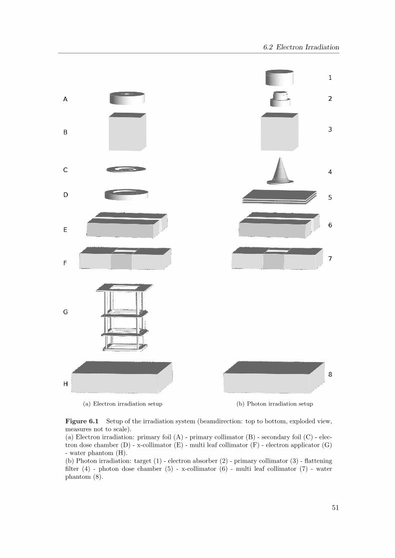
6.2 Electron Irradiation
(a) Electron irradiation setup (b) Photon irradiation setup
Figure 6.1 Setup of the irradiation system (beamdirection: top to bottom, exploded view,measures not to scale).(a) Electron irradiation: primary foil (A) - primary collimator (B) - secondary foil (C) - elec-tron dose chamber (D) - x-collimator (E) - multi leaf collimator (F) - electron applicator (G)- water phantom (H).(b) Photon irradiation: target (1) - electron absorber (2) - primary collimator (3) - flatteningfilter (4) - photon dose chamber (5) - x-collimator (6) - multi leaf collimator (7) - waterphantom (8).
51
6 Simulation Setup
leads to an enlarged penumbra and a less strictly defined irradiation area. The electronapplicators allow the collimation of the electron beam close to the patient, but care hasto be taken of the side leakage of electrons and photons. As more and more objects areinserted in the electron beam, the amount of secondary particles is increasing. Theseadditional particles can deposit dose in healty tissue, which has to be avoided.
6.3 Photon Irradiation
The photon irradiation has to meet similar standards as well as the electron irradiationregarding homogeneity and flatness of the dose inside the irradiation area. As the accel-eration unit is the same as for the electron irradiation, the photons have to be generatedthrough Bremsstrahlung in a target and the remaining electrons have to be suppressedin the irradiation field. The beam is shaped by an energy-dependent flattening filter andcollimated by the main x- and y-collimators. A schematic drawing of the complete photonirradiation configuration is shown in figure 6.1(b).The photons are generated in a transmission target, which is placed in the primary eletronbeam directly behind the exit window. The target is cooled by surrounding water, as alot of the energy of the electrons is transferred to the material in a very small volume.The water cooling is not included in the simulation, as the water is not in the primarybeam and the surrounding materials are strongly absorbing, so the water is not takingpart in the beam shaping or photon generation.Behind the target, an electron absorber is needed to restrain the remaining electrons fromthe patient, as the electrons would lead to an increased skin dose. The photons can eas-ily pass through the absorber, and have to be shaped afterwards. As the distribution isnot homogeneous and flat after the target, a flattening filter is placed in the beam. Theenergy-dependent flattening filter is used to modify the intensity and distribution of thephoton irradiation.Again, the flux of the photons is inspected by a photon dose chamber, which is differentfrom the electron dose chamber due to the different interactions. The dose measured be-tween the flattening filter and the collimation system is included in the feedback controlof the electron acceleration.The medical linear accelerator head has to provide multiple moving parts, as the setuphas to be modified between different irradiation modes. Additionally, the flattening filtersfor the photon irradiation has to be exchanged for different applied energies.
6.4 Data Analysis
In the real setup, the only accessible measure of the irradiation is the applied dose. Thesimulation can rebuild the measurement and then yield additional information. TheMonte-Carlo simulation results in a condensed history for each particle and all secondaryparticles.The main measurement is performed with a water phantom which is placed at the po-sition of the patient. Inside this phantom, the dose can be measured electronically as afunction of depth and lateral displacement. Additionally, films can be placed anywherein the setup, but films can only show the integrated dose distribution weighted with the
52
6.4 Data Analysis
conversion curve which leads to difficult interpretation of the results.In the simulation, the water phantom is also present and the deposited energy is acces-sible as a function of space. Despite the water phantom measurement, different othermeasurements even with films can be modelled, as the trajectories of each particle can bemonitored.Any geometrical object in the simulation can be used as a detector. This allows the ob-servation of multiple measurement volumes within a single simulation. The informationgained for all interactions points inside a registered object is stored during the simulation.When the Monte-Carlo simulation is finished, the stored information can be exportedinto histograms. The typical line scans (depth dose distribution and lateral dose profiles)and area plots (dose distribution in a slice) are realised as one- or two-dimensional his-tograms [42]. The spatial integration over reasonable volumes leads to smooth plots inreasonable computing time.The advantage of the simulation is the availability of additional information like thenumber of particles, the spectral distribution of the particles or even the possibility todistinguish between the dose coming from electrons or photons. These quantities can beextracted from the stored information which is available in any registered volume.
53


7 Results
The following section presents results obtained with the Monte-Carlo tool Geant4 andsome comparisons with measurements. The detailed geometrical dimensions have beendetermined in cooperation with the Siemens AG, Healthcare Sector. Many of the resultsare also part of the diploma thesis by Ina Munster and parts are published in [43]. As herdiploma thesis was supervised by the author of this work, many aspects were observed inclose collaboration.
7.1 Electron Irradiation
Clinical irradiation simulation is used for treatment planning and hence aims for the cal-culation of applied dose inside a treatment volume with a special interest in computationspeed [44]. The dose calculation is based on lookup tables and probability functions [45].In many cases, the Monte-Carlo simulation is starting from a basic model of the irra-diation at the exit of the linear accelerator and is focussing on the dose distribution inmedical samples.The simulation presented in the following starts at the exit window of the energy selectivebending magnet. In contrast to former publications, the simulation is focussing on thebeam characteristics and not on the dose distribution in a medical phantom. The finalcollimation in the electron irradiation is done by the electron applicator. The simulationsare performed for the 20*20 applicator, which limits the irradiated area to a quadraticfield with 20 cm edge length.
7.1.1 Validation of the Simulation
A simulation can only be used for the evaluation of parameters, when the simulated datacoinsides with real measurements. As the dose distribution inside a water phantom isaccessable in the measurement, the simulation yields the same measurand. All incomingparticles in the water phantom lead to deposited energy inside the volume. The depositedenergy is converted into a dose by taking into account the deposition volume. The welldefined depth dose distribution, which can be found in the literature (see figure 5.3), canbe obtained in the central irradiation field. In figure 7.1 the dose distribution as a functionof penetration depth in water is plotted.The simulated data is compared to measurements, which were taken at a medical linearaccelerator in a test cell. The agreement is within the expected range with respect tothe spread between the measurements which is shown for the initial energy of 6 MeV.Additionally, the spectral distribution of the electrons in the measurement is not knownexactly, which can lead to variations in the slope of the curve. But the depth dose maximacoincide very well between measurement and simulation.
55
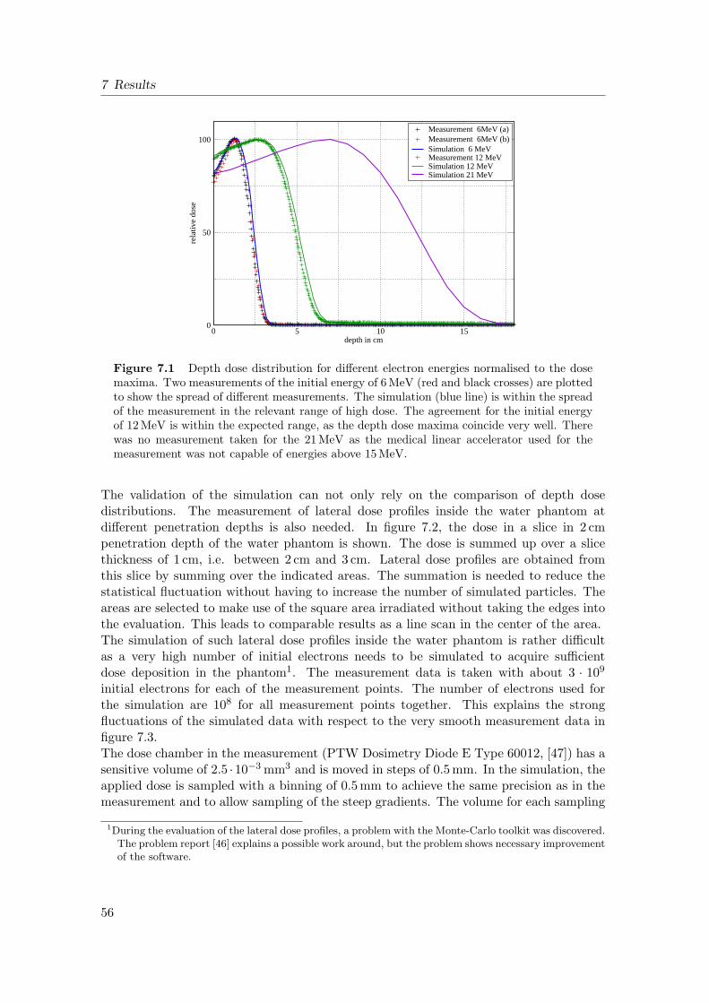
7 Results
0 5 10 15depth in cm
0
50
100
rela
tive
dose
Measurement 6MeV (a)Measurement 6MeV (b)Simulation 6 MeVMeasurement 12 MeVSimulation 12 MeVSimulation 21 MeV
Figure 7.1 Depth dose distribution for different electron energies normalised to the dosemaxima. Two measurements of the initial energy of 6 MeV (red and black crosses) are plottedto show the spread of different measurements. The simulation (blue line) is within the spreadof the measurement in the relevant range of high dose. The agreement for the initial energyof 12 MeV is within the expected range, as the depth dose maxima coincide very well. Therewas no measurement taken for the 21 MeV as the medical linear accelerator used for themeasurement was not capable of energies above 15 MeV.
The validation of the simulation can not only rely on the comparison of depth dosedistributions. The measurement of lateral dose profiles inside the water phantom atdifferent penetration depths is also needed. In figure 7.2, the dose in a slice in 2 cmpenetration depth of the water phantom is shown. The dose is summed up over a slicethickness of 1 cm, i.e. between 2 cm and 3 cm. Lateral dose profiles are obtained fromthis slice by summing over the indicated areas. The summation is needed to reduce thestatistical fluctuation without having to increase the number of simulated particles. Theareas are selected to make use of the square area irradiated without taking the edges intothe evaluation. This leads to comparable results as a line scan in the center of the area.The simulation of such lateral dose profiles inside the water phantom is rather difficultas a very high number of initial electrons needs to be simulated to acquire sufficientdose deposition in the phantom1. The measurement data is taken with about 3 · 109
initial electrons for each of the measurement points. The number of electrons used forthe simulation are 108 for all measurement points together. This explains the strongfluctuations of the simulated data with respect to the very smooth measurement data infigure 7.3.The dose chamber in the measurement (PTW Dosimetry Diode E Type 60012, [47]) has asensitive volume of 2.5 ·10−3 mm3 and is moved in steps of 0.5 mm. In the simulation, theapplied dose is sampled with a binning of 0.5 mm to achieve the same precision as in themeasurement and to allow sampling of the steep gradients. The volume for each sampling
1During the evaluation of the lateral dose profiles, a problem with the Monte-Carlo toolkit was discovered.The problem report [46] explains a possible work around, but the problem shows necessary improvementof the software.
56
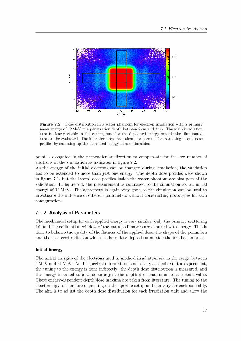
7.1 Electron Irradiation
Figure 7.2 Dose distribution in a water phantom for electron irradiation with a primarymean energy of 12 MeV in a penetration depth between 2 cm and 3 cm. The main irradiationarea is clearly visible in the centre, but also the deposited energy outside the illuminatedarea can be evaluated. The indicated areas are taken into account for extracting lateral doseprofiles by summing up the deposited energy in one dimension.
point is elongated in the perpendicular direction to compensate for the low number ofelectrons in the simulation as indicated in figure 7.2.As the energy of the initial electrons can be changed during irradiation, the validationhas to be extended to more than just one energy. The depth dose profiles were shownin figure 7.1, but the lateral dose profiles inside the water phantom are also part of thevalidation. In figure 7.4, the measurement is compared to the simulation for an initialenergy of 12 MeV. The agreement is again very good so the simulation can be used toinvestigate the influence of different parameters without constructing prototypes for eachconfiguration.
7.1.2 Analysis of Parameters
The mechanical setup for each applied energy is very similar: only the primary scatteringfoil and the collimation window of the main collimators are changed with energy. This isdone to balance the quality of the flatness of the applied dose, the shape of the penumbraand the scattered radiation which leads to dose deposition outside the irradiation area.
Initial Energy
The initial energies of the electrons used in medical irradiation are in the range between6 MeV and 21 MeV. As the spectral information is not easily accessible in the experiment,the tuning to the energy is done indirectly: the depth dose distribution is measured, andthe energy is tuned to a value to adjust the depth dose maximum to a certain value.These energy-dependent depth dose maxima are taken from literature. The tuning to theexact energy is therefore depending on the specific setup and can vary for each assembly.The aim is to adjust the depth dose distribution for each irradiation unit and allow the
57
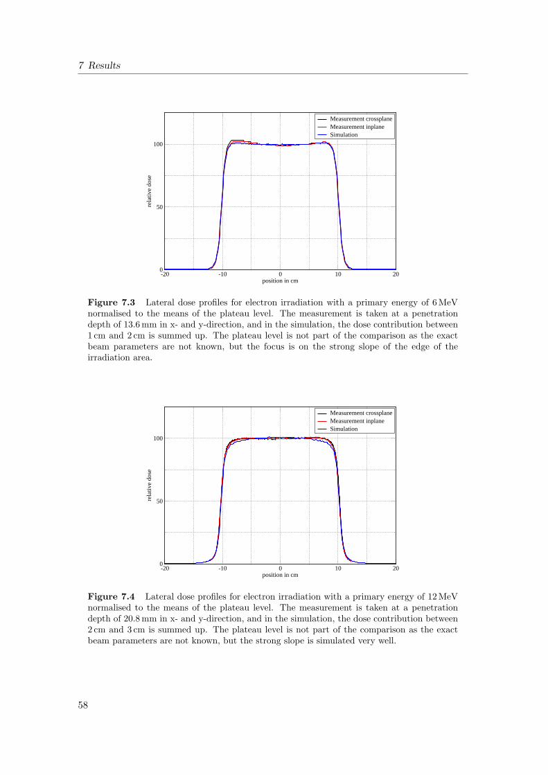
7 Results
-20 -10 0 10 20position in cm
0
50
100re
lativ
e do
se
Measurement crossplaneMeasurement inplaneSimulation
Figure 7.3 Lateral dose profiles for electron irradiation with a primary energy of 6 MeVnormalised to the means of the plateau level. The measurement is taken at a penetrationdepth of 13.6 mm in x- and y-direction, and in the simulation, the dose contribution between1 cm and 2 cm is summed up. The plateau level is not part of the comparison as the exactbeam parameters are not known, but the focus is on the strong slope of the edge of theirradiation area.
-20 -10 0 10 20position in cm
0
50
100
rela
tive
dose
Measurement crossplaneMeasurement inplaneSimulation
Figure 7.4 Lateral dose profiles for electron irradiation with a primary energy of 12 MeVnormalised to the means of the plateau level. The measurement is taken at a penetrationdepth of 20.8 mm in x- and y-direction, and in the simulation, the dose contribution between2 cm and 3 cm is summed up. The plateau level is not part of the comparison as the exactbeam parameters are not known, but the strong slope is simulated very well.
58
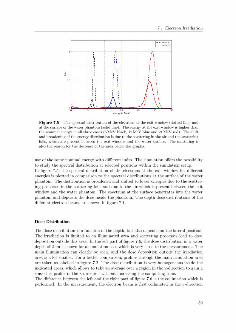
7.1 Electron Irradiation
0 5 10 15 20 25 30energy in MeV
0
0.5
1
a.u.
sourcesurface
Figure 7.5 The spectral distribution of the electrons at the exit window (dotted line) andat the surface of the water phantom (solid line). The energy at the exit window is higher thanthe nominal energy in all three cases (6 MeV black, 12 MeV blue and 21 MeV red). The shiftand broadening of the energy distribution is due to the scattering in the air and the scatteringfoils, which are present between the exit window and the water surface. The scattering isalso the reason for the decrease of the area below the graphs.
use of the same nominal energy with different units. The simulation offers the possibilityto study the spectral distribution at selected positions within the simulation setup.In figure 7.5, the spectral distribution of the electrons at the exit window for differentenergies is plotted in comparison to the spectral distributions at the surface of the waterphantom. The distribution is broadened and shifted to lower energies due to the scatter-ing processes in the scattering foils and due to the air which is present between the exitwindow and the water phantom. The spectrum at the surface penetrates into the waterphantom and deposits the dose inside the phantom. The depth dose distributions of thedifferent electron beams are shown in figure 7.1.
Dose Distribution
The dose distribution is a function of the depth, but also depends on the lateral position.The irradiation is limited to an illuminated area and scattering processes lead to dosedeposition outside this area. In the left part of figure 7.6, the dose distribution in a waterdepth of 2 cm is shown for a simulation case which is very close to the measurement. Themain illumination can clearly be seen, and the dose deposition outside the irradiationarea is a lot smaller. For a better comparison, profiles through the main irradiation areaare taken as labelled in figure 7.2. The dose distribution is very homogeneous inside theindicated areas, which allows to take an average over a region in the y-direction to gain asmoother profile in the x-direction without increasing the computing time.The difference between the left and the right part of figure 7.6 is the collimation which isperformed. In the measurement, the electron beam is first collimated in the y-direction
59
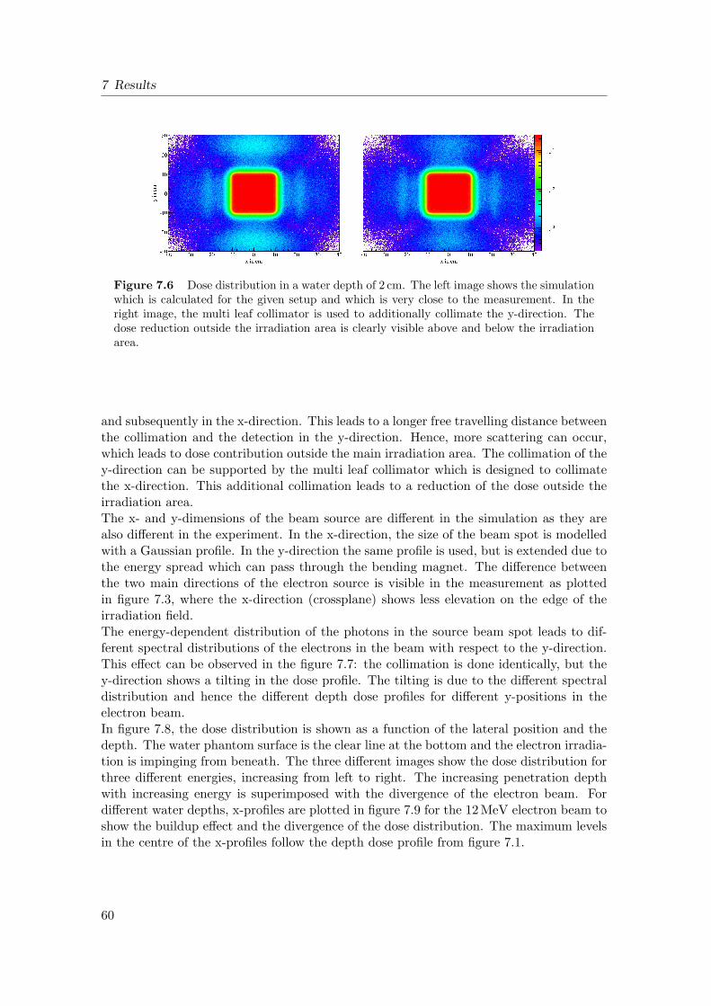
7 Results
Figure 7.6 Dose distribution in a water depth of 2 cm. The left image shows the simulationwhich is calculated for the given setup and which is very close to the measurement. In theright image, the multi leaf collimator is used to additionally collimate the y-direction. Thedose reduction outside the irradiation area is clearly visible above and below the irradiationarea.
and subsequently in the x-direction. This leads to a longer free travelling distance betweenthe collimation and the detection in the y-direction. Hence, more scattering can occur,which leads to dose contribution outside the main irradiation area. The collimation of they-direction can be supported by the multi leaf collimator which is designed to collimatethe x-direction. This additional collimation leads to a reduction of the dose outside theirradiation area.The x- and y-dimensions of the beam source are different in the simulation as they arealso different in the experiment. In the x-direction, the size of the beam spot is modelledwith a Gaussian profile. In the y-direction the same profile is used, but is extended due tothe energy spread which can pass through the bending magnet. The difference betweenthe two main directions of the electron source is visible in the measurement as plottedin figure 7.3, where the x-direction (crossplane) shows less elevation on the edge of theirradiation field.The energy-dependent distribution of the photons in the source beam spot leads to dif-ferent spectral distributions of the electrons in the beam with respect to the y-direction.This effect can be observed in the figure 7.7: the collimation is done identically, but they-direction shows a tilting in the dose profile. The tilting is due to the different spectraldistribution and hence the different depth dose profiles for different y-positions in theelectron beam.In figure 7.8, the dose distribution is shown as a function of the lateral position and thedepth. The water phantom surface is the clear line at the bottom and the electron irradia-tion is impinging from beneath. The three different images show the dose distribution forthree different energies, increasing from left to right. The increasing penetration depthwith increasing energy is superimposed with the divergence of the electron beam. Fordifferent water depths, x-profiles are plotted in figure 7.9 for the 12 MeV electron beam toshow the buildup effect and the divergence of the dose distribution. The maximum levelsin the centre of the x-profiles follow the depth dose profile from figure 7.1.
60
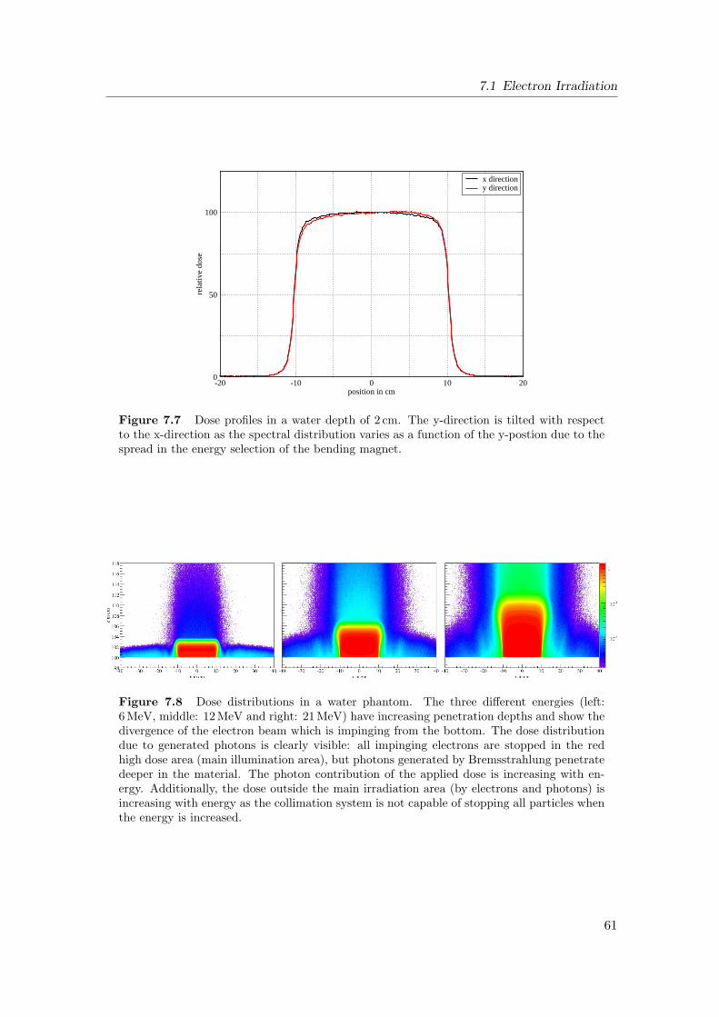
7.1 Electron Irradiation
-20 -10 0 10 20position in cm
0
50
100
rela
tive
dose
x directiony direction
Figure 7.7 Dose profiles in a water depth of 2 cm. The y-direction is tilted with respectto the x-direction as the spectral distribution varies as a function of the y-postion due to thespread in the energy selection of the bending magnet.
Figure 7.8 Dose distributions in a water phantom. The three different energies (left:6 MeV, middle: 12 MeV and right: 21 MeV) have increasing penetration depths and show thedivergence of the electron beam which is impinging from the bottom. The dose distributiondue to generated photons is clearly visible: all impinging electrons are stopped in the redhigh dose area (main illumination area), but photons generated by Bremsstrahlung penetratedeeper in the material. The photon contribution of the applied dose is increasing with en-ergy. Additionally, the dose outside the main irradiation area (by electrons and photons) isincreasing with energy as the collimation system is not capable of stopping all particles whenthe energy is increased.
61
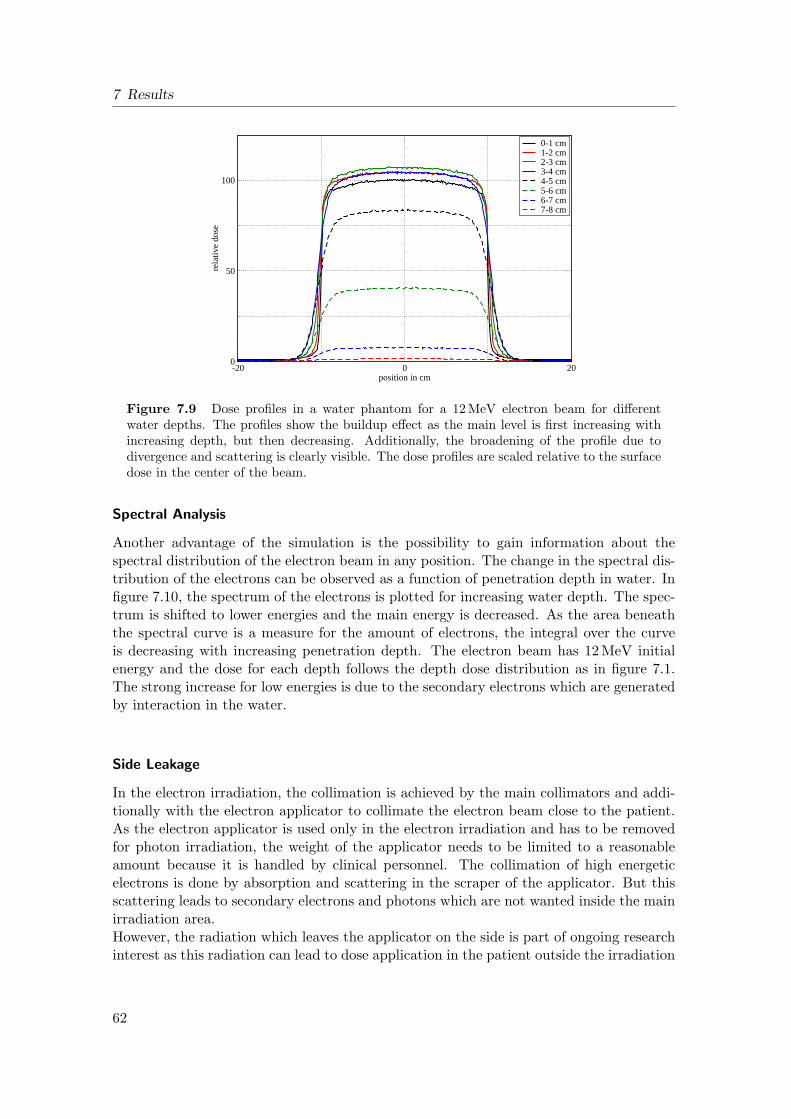
7 Results
-20 0 20position in cm
0
50
100
rela
tive
dose
0-1 cm1-2 cm2-3 cm3-4 cm4-5 cm5-6 cm6-7 cm7-8 cm
Figure 7.9 Dose profiles in a water phantom for a 12 MeV electron beam for differentwater depths. The profiles show the buildup effect as the main level is first increasing withincreasing depth, but then decreasing. Additionally, the broadening of the profile due todivergence and scattering is clearly visible. The dose profiles are scaled relative to the surfacedose in the center of the beam.
Spectral Analysis
Another advantage of the simulation is the possibility to gain information about thespectral distribution of the electron beam in any position. The change in the spectral dis-tribution of the electrons can be observed as a function of penetration depth in water. Infigure 7.10, the spectrum of the electrons is plotted for increasing water depth. The spec-trum is shifted to lower energies and the main energy is decreased. As the area beneaththe spectral curve is a measure for the amount of electrons, the integral over the curveis decreasing with increasing penetration depth. The electron beam has 12 MeV initialenergy and the dose for each depth follows the depth dose distribution as in figure 7.1.The strong increase for low energies is due to the secondary electrons which are generatedby interaction in the water.
Side Leakage
In the electron irradiation, the collimation is achieved by the main collimators and addi-tionally with the electron applicator to collimate the electron beam close to the patient.As the electron applicator is used only in the electron irradiation and has to be removedfor photon irradiation, the weight of the applicator needs to be limited to a reasonableamount because it is handled by clinical personnel. The collimation of high energeticelectrons is done by absorption and scattering in the scraper of the applicator. But thisscattering leads to secondary electrons and photons which are not wanted inside the mainirradiation area.However, the radiation which leaves the applicator on the side is part of ongoing researchinterest as this radiation can lead to dose application in the patient outside the irradiation
62
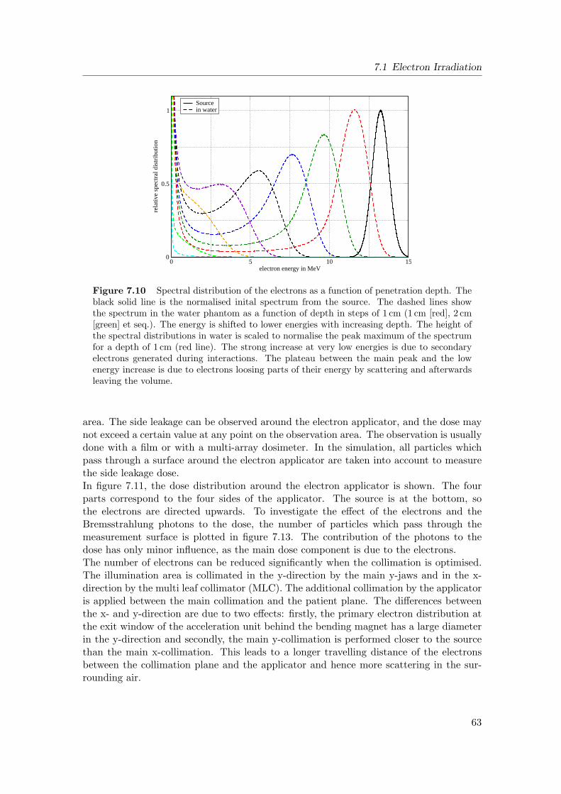
7.1 Electron Irradiation
0 5 10 15electron energy in MeV
0
0.5
1
rela
tive
spec
tral
dis
trib
utio
n
Sourcein water
Figure 7.10 Spectral distribution of the electrons as a function of penetration depth. Theblack solid line is the normalised inital spectrum from the source. The dashed lines showthe spectrum in the water phantom as a function of depth in steps of 1 cm (1 cm [red], 2 cm[green] et seq.). The energy is shifted to lower energies with increasing depth. The height ofthe spectral distributions in water is scaled to normalise the peak maximum of the spectrumfor a depth of 1 cm (red line). The strong increase at very low energies is due to secondaryelectrons generated during interactions. The plateau between the main peak and the lowenergy increase is due to electrons loosing parts of their energy by scattering and afterwardsleaving the volume.
area. The side leakage can be observed around the electron applicator, and the dose maynot exceed a certain value at any point on the observation area. The observation is usuallydone with a film or with a multi-array dosimeter. In the simulation, all particles whichpass through a surface around the electron applicator are taken into account to measurethe side leakage dose.In figure 7.11, the dose distribution around the electron applicator is shown. The fourparts correspond to the four sides of the applicator. The source is at the bottom, sothe electrons are directed upwards. To investigate the effect of the electrons and theBremsstrahlung photons to the dose, the number of particles which pass through themeasurement surface is plotted in figure 7.13. The contribution of the photons to thedose has only minor influence, as the main dose component is due to the electrons.The number of electrons can be reduced significantly when the collimation is optimised.The illumination area is collimated in the y-direction by the main y-jaws and in the x-direction by the multi leaf collimator (MLC). The additional collimation by the applicatoris applied between the main collimation and the patient plane. The differences betweenthe x- and y-direction are due to two effects: firstly, the primary electron distribution atthe exit window of the acceleration unit behind the bending magnet has a large diameterin the y-direction and secondly, the main y-collimation is performed closer to the sourcethan the main x-collimation. This leads to a longer travelling distance of the electronsbetween the collimation plane and the applicator and hence more scattering in the sur-rounding air.
63
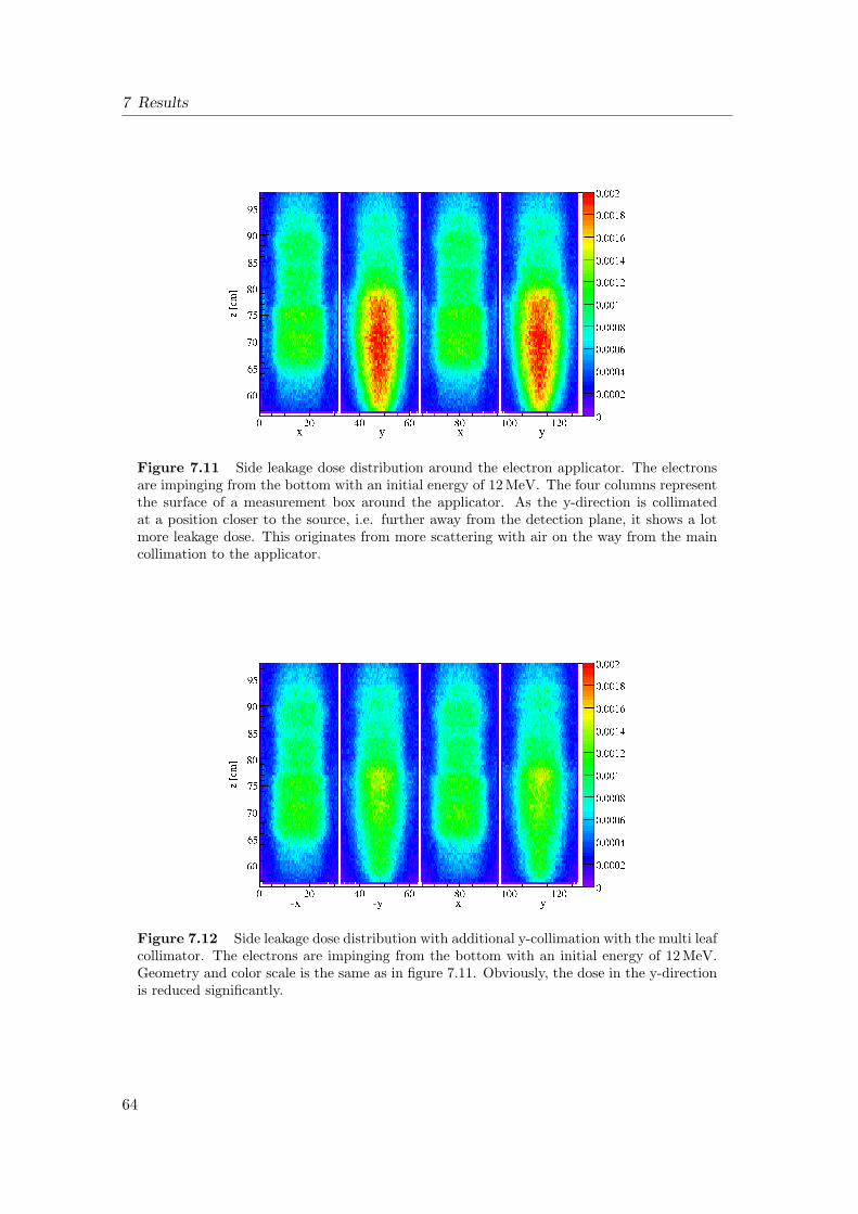
7 Results
Figure 7.11 Side leakage dose distribution around the electron applicator. The electronsare impinging from the bottom with an initial energy of 12 MeV. The four columns representthe surface of a measurement box around the applicator. As the y-direction is collimatedat a position closer to the source, i.e. further away from the detection plane, it shows a lotmore leakage dose. This originates from more scattering with air on the way from the maincollimation to the applicator.
Figure 7.12 Side leakage dose distribution with additional y-collimation with the multi leafcollimator. The electrons are impinging from the bottom with an initial energy of 12 MeV.Geometry and color scale is the same as in figure 7.11. Obviously, the dose in the y-directionis reduced significantly.
64
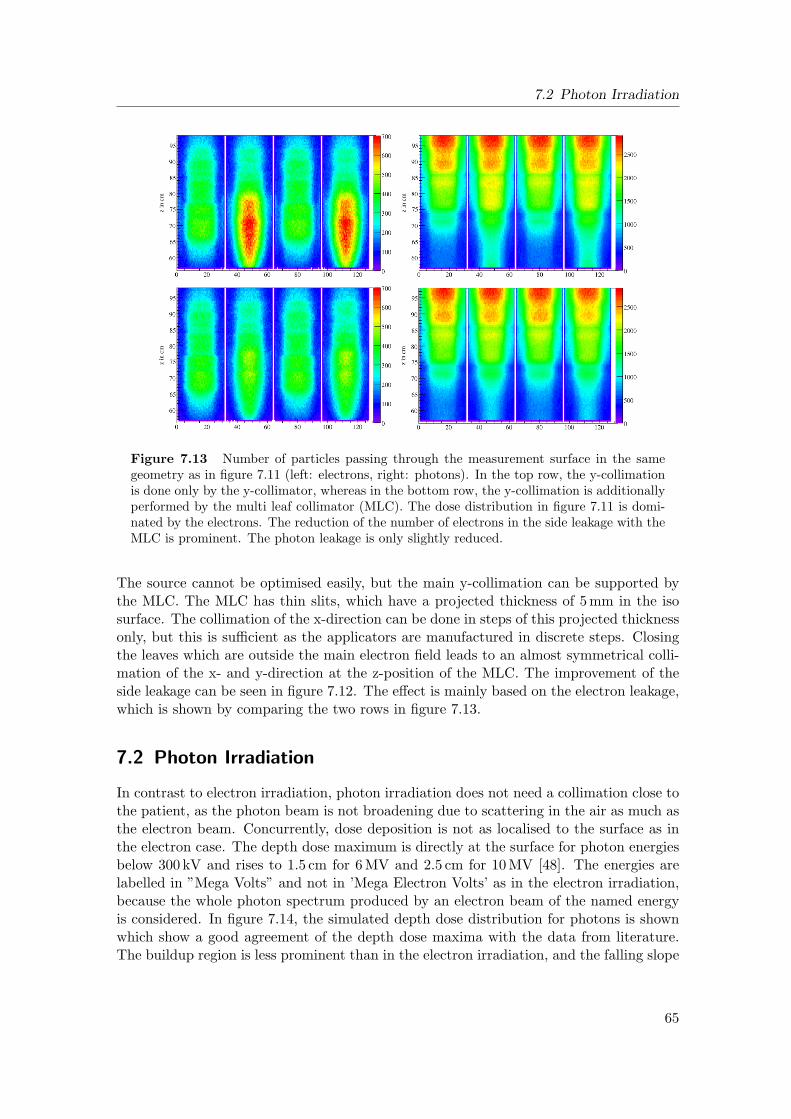
7.2 Photon Irradiation
Figure 7.13 Number of particles passing through the measurement surface in the samegeometry as in figure 7.11 (left: electrons, right: photons). In the top row, the y-collimationis done only by the y-collimator, whereas in the bottom row, the y-collimation is additionallyperformed by the multi leaf collimator (MLC). The dose distribution in figure 7.11 is domi-nated by the electrons. The reduction of the number of electrons in the side leakage with theMLC is prominent. The photon leakage is only slightly reduced.
The source cannot be optimised easily, but the main y-collimation can be supported bythe MLC. The MLC has thin slits, which have a projected thickness of 5 mm in the isosurface. The collimation of the x-direction can be done in steps of this projected thicknessonly, but this is sufficient as the applicators are manufactured in discrete steps. Closingthe leaves which are outside the main electron field leads to an almost symmetrical colli-mation of the x- and y-direction at the z-position of the MLC. The improvement of theside leakage can be seen in figure 7.12. The effect is mainly based on the electron leakage,which is shown by comparing the two rows in figure 7.13.
7.2 Photon Irradiation
In contrast to electron irradiation, photon irradiation does not need a collimation close tothe patient, as the photon beam is not broadening due to scattering in the air as much asthe electron beam. Concurrently, dose deposition is not as localised to the surface as inthe electron case. The depth dose maximum is directly at the surface for photon energiesbelow 300 kV and rises to 1.5 cm for 6 MV and 2.5 cm for 10 MV [48]. The energies arelabelled in ”Mega Volts” and not in ’Mega Electron Volts’ as in the electron irradiation,because the whole photon spectrum produced by an electron beam of the named energyis considered. In figure 7.14, the simulated depth dose distribution for photons is shownwhich show a good agreement of the depth dose maxima with the data from literature.The buildup region is less prominent than in the electron irradiation, and the falling slope
65
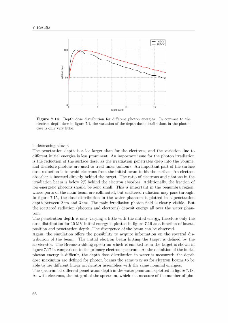
7 Results
0 5 10 15depth in cm
0
50
100
rela
tive
dose
6 MV18 MV
Figure 7.14 Depth dose distribution for different photon energies. In contrast to theelectron depth dose in figure 7.1, the variation of the depth dose distributions in the photoncase is only very little.
is decreasing slower.The penetration depth is a lot larger than for the electrons, and the variation due todifferent initial energies is less prominent. An important issue for the photon irradiationis the reduction of the surface dose, as the irradiation penetrates deep into the volume,and therefore photons are used to treat inner tumours. An important part of the surfacedose reduction is to avoid electrons from the initial beam to hit the surface. An electronabsorber is inserted directly behind the target. The ratio of electrons and photons in theirradiation beam is below 2% behind the electron absorber. Additionally, the fraction oflow-energetic photons should be kept small. This is important in the penumbra region,where parts of the main beam are collimated, but scattered radiation may pass through.In figure 7.15, the dose distribution in the water phantom is plotted in a penetrationdepth between 2 cm and 3 cm. The main irradiation photon field is clearly visible. Butthe scattered radiation (photons and electrons) deposit energy all over the water phan-tom.The penetration depth is only varying a little with the initial energy, therefore only thedose distribution for 15 MV initial energy is plotted in figure 7.16 as a function of lateralposition and penetration depth. The divergence of the beam can be observed.Again, the simulation offers the possibility to acquire information on the spectral dis-tribution of the beam. The initial electron beam hitting the target is defined by theaccelerator. The Bremsstrahlung spectrum which is emitted from the target is shown infigure 7.17 in comparison to the primary electron spectrum. As the definition of the initialphoton energy is difficult, the depth dose distribution in water is measured: the depthdose maximum are defined for photon beams the same way as for electron beams to beable to use different linear accelerator assemblies with the same nominal energies.The spectrum at different penetration depth in the water phantom is plotted in figure 7.18.As with electrons, the integral of the spectrum, which is a measure of the number of pho-
66
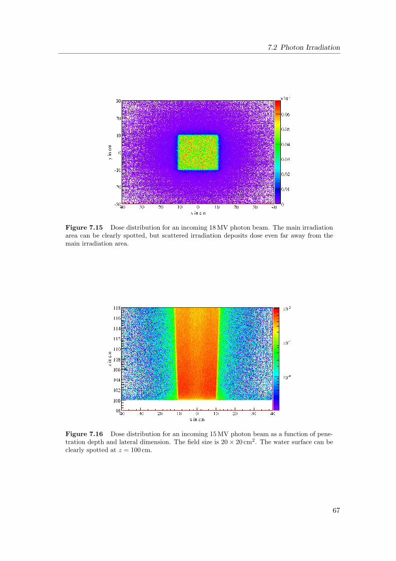
7.2 Photon Irradiation
Figure 7.15 Dose distribution for an incoming 18 MV photon beam. The main irradiationarea can be clearly spotted, but scattered irradiation deposits dose even far away from themain irradiation area.
Figure 7.16 Dose distribution for an incoming 15 MV photon beam as a function of pene-tration depth and lateral dimension. The field size is 20× 20 cm2. The water surface can beclearly spotted at z = 100 cm.
67
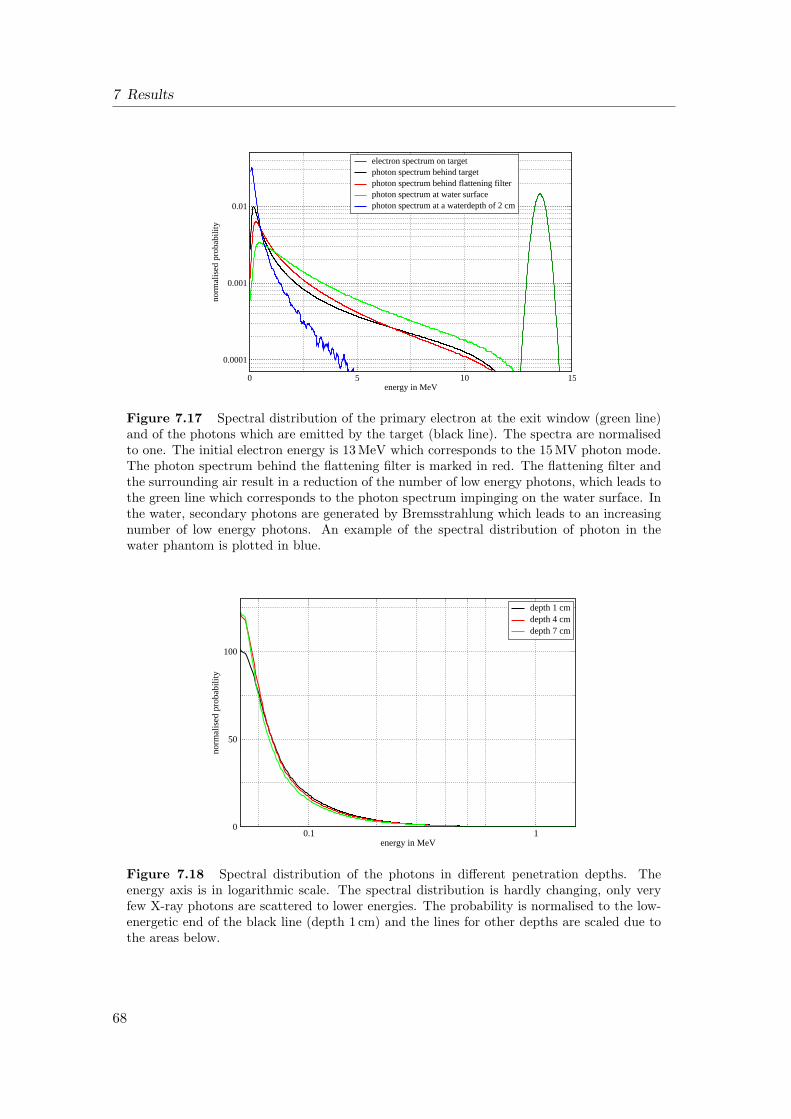
7 Results
0 5 10 15energy in MeV
0.0001
0.001
0.01no
rmal
ised
pro
babi
lity
electron spectrum on targetphoton spectrum behind targetphoton spectrum behind flattening filterphoton spectrum at water surfacephoton spectrum at a waterdepth of 2 cm
Figure 7.17 Spectral distribution of the primary electron at the exit window (green line)and of the photons which are emitted by the target (black line). The spectra are normalisedto one. The initial electron energy is 13 MeV which corresponds to the 15 MV photon mode.The photon spectrum behind the flattening filter is marked in red. The flattening filter andthe surrounding air result in a reduction of the number of low energy photons, which leads tothe green line which corresponds to the photon spectrum impinging on the water surface. Inthe water, secondary photons are generated by Bremsstrahlung which leads to an increasingnumber of low energy photons. An example of the spectral distribution of photon in thewater phantom is plotted in blue.
0.1 1energy in MeV
0
50
100
norm
alis
ed p
roba
bilit
y
depth 1 cmdepth 4 cmdepth 7 cm
Figure 7.18 Spectral distribution of the photons in different penetration depths. Theenergy axis is in logarithmic scale. The spectral distribution is hardly changing, only veryfew X-ray photons are scattered to lower energies. The probability is normalised to the low-energetic end of the black line (depth 1 cm) and the lines for other depths are scaled due tothe areas below.
68

7.2 Photon Irradiation
tons, follows the depth dose distribution in figure 7.14. In contrast to the electron case,the spectrum is not changing significantly.For photon irradiation, the multi leaf collimator can be used to form the irradiation area.It is possible to limit the beam to the shape of the tumour and so protect surroundingtissue from being irradiated. This is important due to the high penetration of photons inthe human tissue.
69

8 Summary and Discussion of Part II
The simulation of the medical irradiation module with the Monte-Carlo tool Geant4 offersthe possibility to follow each individual particle on its passage through matter. This directaccess to the trajectory of the particles is a powerful tool to gain more information on thesystem. In contrast to the clinical Monte-Carlo simulation, the focus of the evaluationwas not set to the applied dose to a patient, but to the observation of the characteristicsof the irradiation head.
The photon irradiation mode simulation was build up based on the technical detailsof the manufactured parts in the beam line. The simulation starts with the impingingelectrons and the photon generation in the target is modelled. The flattening filter andthe beam collimation are part of the simulation as well. The depth dose curves show goodagreement with the data from literature as shown in figure 7.14. The distributions of theimpinging particles on the water surface are a kind of information which is not accessiblein the measurement. The possibility to distinguish between electron and photon contri-bution to the dose can lead to an improved knowledge on the initial particle distributionin the measurement and show ways to improve the photon distribution.The dose distribution in figure 7.16 shows the need for multifield irradiation in the caseof photon irradiation. As the dose deposition is very homogeneous with increasing depth,the dose can be increased in the target volume, i.e. the tumour, by irradiating fromdifferent directions. This is part of the dose planning systems which are used in clinicalenvironments. But these dose planning systems need to have a detailed knowledge on theparticle beam which is coming out of the accelerator. The simulation allows to study notonly the dose distribution but also the spectral changes when the beam path is modifiedeither by collimation or inserting scattering parts. The spectral study can improve themodel of the accelerator head used in the dose planning systems.
The electron simulation contains a detailed model of the experimental setup. This al-lows the validation of the simulation by direct comparison of the simulation and themeasurement results. The agreement between the simulated and measured dose distribu-tions is very good as pointed out in figures 7.1 and 7.3. This encourages the evaluation ofpossible improvements of the electron irradiation. As shown in figure 7.6 the dose outsidethe irradiation area can be reduced by applying the multi leaf collimator (MLC). Theadditional collimation of the y-direction reduces the dose without disturbing the qualityof the beam inside the irradiation area.The reduction of the dose outside the main illumination area is also clearly visible in thedose contribution which leaves the electron applicator at the side. Any particle leavingthe applicator on the side is on the one hand lost for the main irradiation purpose andcan on the other hand deposit its energy in sensitive healthy regions of the patient. Theclosing of the MLC leads to less particles leaving the electron applicator without affecting
71

8 Summary and Discussion of Part II
the flatness of symmetry of the main irradiation beam.Information which is hardly available in the measurement is the spectral distribution ofthe particles in the beam. The knowledge of the spectral components and particle sortsat certain positions can be used to improve the collimation efficiency, as electrons canbe stopped by light materials whereas photons are only attenuated. The electrons areadditionally collimated by the electron applicator, but in the photon mode no applicatoris needed. This requires the mounting and dismounting of the electron applicator for eachirradiation procedure. The weight of the electron applicator is therefore competing withthe collimation efficiency. In the diploma thesis of Ina Munster, the weight reduction ofthe electron applicator is part of the topic.
The simulation is built up to a stage where effective studies on collimation and beamshaping parts can be performed. Additional information gained with the simulation canbe used to optimise the setup and develop future medical irradiation systems.
72

Summary
This thesis aims for an improved understanding of medical irradiation. Two major partsare investigated: the beam shaping components of a medical linear accelerator, i.e. thesource of the radiation, and the signal generation inside semiconductor sensors, i.e. thedetection of the radiation.
The direct measurement of the spatial and spectral particle distribution in the irradiationbeam is not possible with state of the art detectors due to the high particle flux. Thedevelopment of new advanced detectors is the goal of the first part of this thesis. Thefocus is set on the signal generation inside the sensor volume of a semiconductor detector.Incoming particles interact with the sensor material and generate clouds of electron holepairs. These pairs get separated by an applied bias voltage. The motion of the chargeclouds is simulated with a finite element programme taking into account the drift anddiffusion.Mirror charges are induced on the electrodes which move due to the motion of the chargecloud. The motion of the induced mirror charges leads to the signal that is detected.The transient calculation of the signals is based on Ramo’s theorem. The efficient adjointformulation of the induction solution is adjusted to doped materials, as for example theelectric bias field and hence the motion of the charge cloud is changing with the dopinglevel. The effect of the doping of the material on the signal shape is shown together withinfluences of different voltages and pixel geometries.Smaller pixels and higher bias voltages can lead to shorter signals which is preferable forhigh flux measurements. Possible count rate improvements are limited by electric breakthrough, high dark current across the sensor layer and charge sharing. Another option toshorten the signals is the use of steering grid electrodes which modify the electric and theweighting field. This results in shorter signals and thus in a higher possible rate.
The detailed Monte-Carlo simulation of the irradiation head of the medical linear accel-erator is constructed for the irradiation with electrons and photons in the second part ofthis thesis. The simulation is validated by comparison with water phantom measurements.Available information from the measurements is limited to the depth dose deposition anddose profiles in selected water depths. The simulation allows the evaluation of dose de-positions and spectral particle distributions at various locations. This will be used tooptimise scattering foils and collimation geometries.In the electron irradiation mode, a collimation close to the patient is performed by anelectron applicator. The leakage radiation at the outside of the applicator needs to remain
73
8 Summary and Discussion of Part II
below certain legal requirements. A possible reduction of the side leakage is evaluatedby optimising the collimation of the beam. This can be achieved with the collimationsystem which is already part of the irradiation head and no additional components arerequired. Additionally, new beam shaping components can be designed and tested beforeprototyping. The influence of fabrication tolerances can also be evaluated.
Together, both parts of this thesis can help to improve the tumour treatment as cancerousdiseases affect a growing number of human beings. Medical irradiation with MeV-electronsand X-ray photons is the part of the clinical tumour treatment which is evaluated in thiswork. Both types of irradiation deposit energy inside the tumour cells and lead to lethaldamages of the DNA inside the cells’ nucleus. For a successful treatment it is crucial toforce all tumour cells into apoptosis while keeping healthy surrounding cells alive. Thisrequires the exact planning of the dose deposition inside the volume, which can only bebased on a detailed knowledge of the irradiation beam.
74
Zusammenfassung
Diese Arbeit zielt auf ein besseres Verstandnis der medizinischen Bestrahlung ab. Dafurwerden zwei Themenbereiche untersucht: die strahlformenden Elemente des medizinischenLinearbeschleunigerkopfes, das heißt die Quelle der Strahlung, und die Signalerzeugungin einem Halbleitersensor, das bedeutet die Detektion der Strahlung.
Die direkte Messung der raumlichen und spektralen Teilchenverteilung im Bestrahlungs-feld ist mit aktuell verfugbaren Detektoren wegen des sehr hohen Teilchenflusses leidernicht moglich. Die Weiterentwicklung von Detektoren ist Thema des ersten Teils der Ar-beit. Der Fokus liegt dabei auf der Erzeugung von Signalen im Sensorvolumen eines Hal-bleiterdetektors. Einfallende Teilchen wechselwirken mit dem Sensormaterial und erzeu-gen Elektron-Loch-Paare am Wechselwirkungsort. Diese Ladungspaare werden durch einanliegendes elektrisches Potential getrennt und bewegen sich auf die entsprechenden Elek-troden zu. Die Bewegung der Ladungswolken wird in einem Finite-Elemente-Programmunter Berucksichtigung von Drift und Diffusion berechnet.Auf den Elektroden werden Spiegelladungen influenziert, die sich entsprechend der Bewe-gung der Ladungswolke im Sensorvolumen verschieben. Die Bewegung der influenziertenSpiegelladungen fuhrt zu einem Signal, das mit einer Ausleseelektronik detektiert wird.Die zeitabhangige Berechnung der Signale basiert auf dem Theorem von Ramo. Die ef-fiziente adjungierte Formulierung der Influenzierung wird fur die Anwendung in dotiertenMaterialen angepasst, da sich durch die Dotierung das elektrische Feld im Sensor unddadurch die Bewegung der Ladungswolke verandert. Der Einfluss der Dotierung auf dieSignalform wird zusammen mit weiteren Einflussen wie verschiedenen Verarmungsspan-nungen und Pixelgeometrien gezeigt.Kleine Pixel und hohe Verarmungsspannungen fuhren zu kurzen Signalen, die fur eineMessung mit hoher Rate notwendig sind. Die moglichen Verbesserungen der Messrate istjedoch durch elektrische Uberschlage, hohe Dunkelstrome durch das Sensormaterial undLadungsverteilung auf mehrere Pixel (charge sharing) begrenzt. Eine weitere Moglichkeitdie Signale zu verkurzen, ist die Verwendung von Steering-Grid-Elektroden, mit denendas elektrische Feld und das Wichtungspotential beeinflusst werden konnen. Dies fuhrtzu kurzeren Signalen und folglich zu der Erreichbarkeit hoherer Messraten.
Fur die Elektronen- und Photonenbestrahlung wird im zweiten Teil der Arbeit eine de-tailierte Monte-Carlo Simulation des Bestrahlungskopfes eines medizinischen Linearbeschle-unigers aufgebaut. Die Validierung der Simulation wird durch den Vergleich mit Messun-gen am Wasserphantom durchgefuhrt. Die Ergebnisse der Messung sind allerdings auf
75

die Tiefendosisverteilung und Dosisprofile in verschiedenen Wassertiefen beschrankt. Beider Auswertung der Simulation kann die raumliche und spektrale Teilchenverteilung anbeliebigen Orten im Simulationsvolumen bestimmt werden. Dies ermoglicht die Opti-mierung von Streufolien und Kollimatorgeometrien.Im Elektronenmodus wird die letzte Kollimierung erst kurz vor der Patientenebene miteinem Elektronenapplikator durchgefuhrt. Die Leckstrahlung, die den Applikator seitlichverlasst, muss gesetzlichen Bestimmungen entsprechen. Eine Variante zur Reduktion derLeckstrahlung wird mit Hilfe der im Bestrahlungskopf vorhandenen Kollimatorkompo-nenten vorgestellt. In diesem Fall sind keine zusatzlichen Komponenten erforderlich, aberneue strahlformende Elemente konnen entwickelt und getestet werden, ohne Prototypenfur das reale Experiment herstellen zu mussen. Es kann auch der Einfluss von Herstel-lungstoleranzen untersucht werden.
Zusammen konnen die beiden Teile der Arbeit helfen, die Tumorbehandlung zu verbessern,was immer wichtiger wird, da die diagnostizierten Krebsneuerkrankungen stetig steigen.Medizinische Bestrahlung mit MeV-Elektronen und Rontgenphotonen ist der Teil der klin-ischen Tumorbehandlung, welcher in dieser Arbeit behandelt wird. Beide Strahlungsartendeponieren Energie in den Tumorzellen, was zu letalen Schaden an der DNA fuhrt. Fur dieerfolgreiche Behandlung ist es notwendig, alle Tumorzellen in die Apoptose zu uberfuhrenund dabei die umgebenden gesunden Zellen zu schutzen. Dies verlangt die genaue Planungder deponierten Dosis im bestrahlten Volumen, was nur auf der detailierten Kenntnis desTeilchenstrahls beruhen kann.

Bibliography
[1] X. Llopart, M. Campbell, R. Dinapoli, D. San Segundo, and E. Pernigotti, “Medipix2:A 64-k pixel readout chip with 55-µm square elements working in single photoncounting mode,” IEEE Trans. Nucl. Sci., vol. 49, no. 5, pp. 2279–2283, 2002.
[2] K.-F. Pfeiffer, Evaluation of the Medipix Detectors for Medical X-Ray Imaging, withSpecial Consideration of Mammography. PhD thesis, Universitat Erlangen-Nurnberg,Dec. 2004.
[3] J. Durst, Modellierung und Simulation physikalischer Eigenschaften photonenzahlen-der Rontgenpixeldetektoren fur die Bildgebung. PhD thesis, Unversitat Erlangen-Nurnberg, July 2008.
[4] R. Ballabriga, M. Campbell, E. Heijne, X. Llopart, and L. Tlustos, “The Medipix3Prototype, a Pixel Readout Chip Working in Single Photon Counting Mode WithImproved Spectrometric Performance,” IEEE Trans. Nucl. Sci., vol. 54, pp. 1824–1829, Oct. 2007.
[5] S. Sze, Semiconductor Devices - Physics and Technology. John Wiley & Sons, Inc.,2 ed., 2002.
[6] A. Zumbiehl, M. Hage-Ali, P. Fougeres, J. Koebel, R. Regal, and P. Siffert, “Electricfield distribution in CdTe and Cd1−xZnxTe nuclear detectors,” Journal of CrystalGrowth, vol. 197, pp. 650–654, 1999.
[7] A. Cola, I. Farella, N. Auricchio, and E. Caroli, “Investigation of the electric fielddistribution in x-ray detectors by Pockels effect,” Journal of Optics A, vol. 8, pp. 467–472, 2006.
[8] S. Ramo, “Currents induced by electron motion,” Proceedings of the I.R.E., vol. 27,pp. 584–585, 1939.
[9] W. Shockley, “Currents to Conductors Induced by a Moving Point Charge,” Journalof Applied Physics, vol. 9, pp. 635–636, 1938.
[10] C. Canali, M. Martini, and G. Ottaviani, “Transport Properties of CdTe,” Phys.Rev. B, vol. 4/2, pp. 422–431, 1971.
[11] A. Korn, Spektrale und bildgebende Eigenschaften photonenzahlender Rontgendetek-toren am Beispiel des Medipix-Detektors. PhD thesis, Universitat Erlangen-Nurn-berg, May 2007.
[12] B. Kreisler, G. Anton, J. Durst, and T. Michel, “Charge Carrier Motion in Semi-conductors,” in Proceedings of the COMSOL Users Conference Frankfurt, pp. 64-66,2006.
77

Bibliography
[13] V. Radeka, “Low-Noise Techniques in Detectors,” Annual Review of Nuclear andParticle Science, vol. 38, pp. 217–277, Dec. 1988.
[14] B. Kreisler, “Influenzierte Signale in pixelierten Halbleiter-Rontgen-Detektoren,”Master’s thesis, Universitat Erlangen-Nurnberg, May 2006.
[15] T. H. Prettyman, “Method for mapping charge pulses in semiconductor radiationdetectors,” Nucl. Instr. and Meth. A, vol. 422, pp. 232–237, Feb. 1999.
[16] G. I. Bell and S. Glasstone, Nuclear reactor theory. Van Nostrand Reinhold Co., NewYork, 1970.
[17] G. Arfken and H. Weber, Essential Mathematical Methods for Physicists. Har-court/Academic Press, Burlington (MA), 2003.
[18] M. Balda, D. Niederlohner, B. Heismann, B. Kreisler, and J. Durst, “Lookup Table-Based Simulation for Direct-Converting Counting X-Ray Detectors for CT,” in Nu-clear Science Symposium Conference Record, IEEE, 2009. Manuscript accepted, tobe published January 2010.
[19] Personal communication with K. Mecke, Universitat Erlangen-Nurnberg, 2008.
[20] B. Kreisler, G. Anton, J. Durst, and T. Michel, “Generalised adjoint simulation ofinduced signals in semiconductor X-ray pixel detectors,” Journal of Instrumentation,vol. 3 P11002, 2008.
[21] COMSOL AB, Stockholm. www.comsol.de (October 2009).
[22] S. Patankar, Numerical heat transfer and fluid flow. Hemisphere Publishing Corpo-ration, Washington, 1980.
[23] B. Kreisler, G. Anton, J. Durst, and T. Michel, “3D simulation of induced signalsin the Medipix detector,” in Nuclear Science Symposium Conference Record, IEEE,2007.
[24] E. Gatti, A. Longoni, P. Rehak, and M. Sampietro, “Dynamics of Electrons in DriftDetectors,” Nucl. Instr. and Meth. A, vol. 253, pp. 393–399, 1987.
[25] The MathWorks, Inc. www.mathworks.de (October 2009).
[26] J. Fink, H. Kruger, P. Lodomez, and N. Wermes, “Characterization of charge col-lection in CdTe and CZT using the transient current technique,” Nucl. Instr. andMeth. A, vol. 560, pp. 435–443, 2006.
[27] Personal communication with D. Niederlohner, Siemens AG, Healthcare Sector, 2009.
[28] International Commission on Radiological Protection, “103: Recommendations ofthe ICRP,” Feb. 2008.
[29] R. L. Morin, T. C. Gerber, and C. H. McCollough, “Radiation Dose in ComputedTomography of the Heart,” Circulation, vol. 107, pp. 917–922, 2003.
78

Bibliography
[30] T. Herrmann and M. Baumann, Klinische Strahlenbiologie: kurz und bundig. GustavFischer Verlag, Jena, 1997.
[31] R. Sauer, Strahlentherapie und Onkologie. Urban&Fischer Verlag, Munchen, 4 ed.,2003.
[32] H. Nagasawa and J. Little, “Induction of Sister Chromatid Exchanges by ExtremelyLow Doses of α-Particles,” Cancer Research, vol. 52, pp. 6394–6396, Nov. 1992.
[33] H. Krieger, Strahlenphysik, Dosimetrie und Strahlenschutz, vol. 1. Teubner,Stuttgart, 1998.
[34] P. Andreo and A. Brahme, “Mean energy in electron beams,” Med. Phys., vol. 8,pp. 682–687, 1981.
[35] P. Andreo, “Depth dose and stopping power data for monoenergetic electron beams,”Nucl. Instr. Meth. B, vol. 51, pp. 107–121, 1990.
[36] H. Krieger, Strahlenphysik, Dosimetrie und Strahlenschutz, vol. 2. Teubner,Stuttgart, 1997.
[37] G. C. Bentel, Radiation therapy planning. McGraw-Hill Companies, Inc., 2 ed., 1996.
[38] S. Agostinelli, J. Allison, K. Amako, J. Apostolakis, H. Araujo, P. Arce, M. Asai,D. Axen, S. Banerjee, G. Barrand, F. Behner, L. Bellagamba, J. Boudreau, L. Broglia,A. Brunengo, H. Burkhardt, S. Chauvie, J. Chuma, R. Chytracek, G. Cooperman,G. Cosmo, P. Degtyarenko, A. Dell’Acqua, G. Depaola, D. Dietrich, R. Enami, A. Fe-liciello, C. Ferguson, H. Fesefeldt, G. Folger, F. Foppiano, A. Forti, S. Garelli, S. Gi-ani, R. Giannitrapani, D. Gibin, J. J. G. Cadenas, I. Gonzalez, G. G. Abril, G. Greeni-aus, W. Greiner, V. Grichine, A. Grossheim, S. Guatelli, P. Gumplinger, R. Hamatsu,K. Hashimoto, H. Hasui, A. Heikkinen, A. Howard, V. Ivanchenko, A. Johnson,F. W. Jones, J. Kallenbach, N. Kanaya, M. Kawabata, Y. Kawabata, M. Kawaguti,S. Kelner, P. Kent, A. Kimura, T. Kodama, R. Kokoulin, M. Kossov, H. Kurashige,E. Lamanna, T. Lampen, V. Lara, V. Lefebure, F. Lei, M. Liendl, W. Lockman,F. Longo, S. Magni, M. Maire, E. Medernach, K. Minamimoto, P. M. de Freitas,Y. Morita, K. Murakami, M. Nagamatu, R. Nartallo, P. Nieminen, T. Nishimura,K. Ohtsubo, M. Okamura, S. O’Neale, Y. Oohata, K. Paech, J. Perl, A. Pfeiffer,M. G. Pia, F. Ranjard, A. Rybin, S. Sadilov, E. D. Salvo, G. Santin, T. Sasaki,N. Savvas, Y. Sawada, S. Scherer, S. Sei, V. Sirotenko, D. Smith, N. Starkov,H. Stoecker, J. Sulkimo, M. Takahata, S. Tanaka, E. Tcherniaev, E. S. Tehrani,M. Tropeano, P. Truscott, H. Uno, L. Urban, P. Urban, M. Verderi, A. Walkden,W. Wander, H. Weber, J. P. Wellisch, T. Wenaus, D. C. Williams, D. Wright, T. Ya-mada, H. Yoshida, and D. Zschiesche, “Geant4 - a simulation toolkit,” Nucl. Instr.and Meth. A, vol. 506, pp. 250–303, 2003.
[39] J. Allison, K. Amako, J. Apostolakis, H. Araujo, P. Dubois, M. Asai, G. Barrand,R. Capra, S. Chauvie, R. Chytracek, G. Cirrone, G. Cooperman, G. Cosmo, G. Cut-tone, G. Daquino, M. Donszelmann, M. Dressel, G. Folger, F. Foppiano, J. Generow-icz, V. Grichine, S. Guatelli, P. Gumplinger, A. Heikkinen, I. Hrivnacova, A. Howard,
79

Bibliography
S. Incerti, V. Ivanchenko, T. Johnson, F. Jones, T. Koi, R. Kokoulin, M. Kossov,H. Kurashige, V. Lara, S. Larsson, F. Lei, O. Link, F. Longo, M. Maire, A. Mantero,B. Mascialino, I. McLaren, P. Lorenzo, K. Minamimoto, K. Murakami, P. Nieminen,L. Pandola, S. Parlati, L. Peralta, J. Perl, A. Pfeiffer, M. Pia, A. Ribon, P. Ro-drigues, G. Russo, S. Sadilov, G. Santin, T. Sasaki, D. Smith, N. Starkov, S. Tanaka,E. Tcherniaev, B. Tome, A. Trindade, P. Truscott, L. Urban, M. Verderi, A. Walk-den, J. Wellisch, D. Williams, D. Wright, and H. Yoshida, “Geant4 Developmentsand Applications,” IEEE Trans. Nucl. Sci., vol. 53, no. 1, pp. 270–278, 2006.
[40] S. Chauvie, S. Guatelli, V. Ivanchenko, F. Longo, A. Mantero, B. Mascialino,P. Nieminen, L. Pandola, S. Parlati, L. Peralta, M. G. Pia, M. Piergentili, P. Ro-drigues, S. Saliceti, and A. Trindade, “Geant4 Low Energy Electromagnetic Physics,”in Nuclear Science Symposium Conference Record, IEEE, 2004.
[41] www.cern.ch/geant4 (October 2009).
[42] P. Mayles, A. E. Nahum, and J.-C. Rosenwald, eds., Handbook of radiotherapyphysics: theory and practice. CRC Press, Taylor & Francis Group, 2007.
[43] I. Munster, B. Kreisler, J. Durst, T. Michel, and G. Anton, “Simulation of a MedicalLinac with Evaluation of Dose Profiles behind an Electron Applicator,” in NuclearScience Symposium Conference Record, IEEE, 2009. Manuscript accepted, to bepublished January 2010.
[44] A. Trindade, P. Rodrigues, L. Peralta, M. Lopes, C. Alves, and A. Chaves, “Fastelectron beam simulation and dose calculation in radiotherapy,” Nucl. Instr. andMeth. A, vol. 522, pp. 568–578, 2004.
[45] F. M. Khan, P. D. Higgins, B. J. Gerbi, F. C. Deibel, A. Sethi, and D. N. Mihailidis,“Calculation of depth dose and dose per monitor uni for irregular shaped electronfields,” Phys. Med. Biol., vol. 43, pp. 2741–2754, 1998.
[46] http://bugzilla-geant4.kek.jp/show bug.cgi?id=1027 (October 2009).
[47] Physikalisch-Technische Werkstatten Dr. Pychlau GmbH, Freiburg, www.ptw.de (Oc-tober 2009).
[48] E. B. Podgorsak, Radiation physics for medical physicists. Springer Verlag, BerlinHeidelberg New York, 2006.
80

Acknowledgements
Just before the end of this manuscript, I will take the chance to thank all the people whomade my time at the institute worthwhile and contributed to this work in one way oranother.Let me begin with my supervisor Gisela Anton who always had her door open to me. Itwas a great opportunity to discuss about physics, but also different topics. Thank youfor the time and the confidence.But all the research presented in this work would have been very hard if not impossiblewithout the support of my colleagues here at the ECAP (Erlangen Centre for AstroparticlePhysics). I would like to point out some who are especially important for me: first of all,I have to express my gratitude to my two diploma students, Ina and Sebastian, not onlyfor the valueable discussions on their topics, but also for the great atmosphere. Secondly,Jurgen has played a vital rule in the success of the work, as he always stayed close to theleading edge of my research and was a great help in many ways.The medical physics group is steadily growing, so I cannot mention everybody indiviually,but there are a few with who I have shared many things while working here: Peter, Mike,Anja, Kati and Claudio. I must not miss the ones who left the institute in the last fewyears and still stay close: Markus & Karo, Frank & Susan. Thank you all for the time inand around the institute.Thanks for the financial support by the International Max-Planck Research School forOptics and Imaging (IMPRS-OI). A special thanks also goes to our collaboration partnersfor their academic and personal interest in my work: Daniel, Silke, Bjorn, Gaby andTorsten.I owe a lot to my parents and my entire family who always encouraged and supported me,so nothing would have been possible without them. And finally, I thank Annelen for a lotmore than I can write down here.
81