Embed Size (px)
Citation preview

Title Enhanced absorption and emission of Y_3Al_5O_12:Ce^[3+]thin layers prepared by epoxide-catalyzed sol-gel method
Author(s)Murai, Shunsuke; Verschuuren, Marc A.; Lozano, Gabriel;Pirruccio, Giuseppe; Koenderink, A. Femius; Rivas, JaimeGómez
Citation Optical Materials Express (2012), 2(8): 1111-1120
Issue Date 2012
URL http://hdl.handle.net/2433/160367
Right
© 2012 Optical Society of America. This paper was publishedin "Optical Materials Express" and is made available as anelectronic reprint with the permission of OSA. The paper canbe found at the following URL on the OSA website:http://www.opticsinfobase.org/ome/abstract.cfm?uri=ome-2-8-1111. Systematic or multiple reproduction or distribution tomultiple locations via electronic or other means is prohibitedand is subject to penalties under law.
Type Journal Article
Textversion publisher
Kyoto University
Enhanced absorption and emission of Y3Al5O12:Ce3+ thin layers prepared by
epoxide-catalyzed sol-gel method
Shunsuke Murai,1,2,* Marc A. Verschuuren,3 Gabriel Lozano,1 Giuseppe Pirruccio,1 A. Femius Koenderink,1 and Jaime Gómez Rivas1,4
1Center for Nanophotonics, FOM Institute AMOLF, c/o Philips Research Laboratories, High Tech Campus 4, 5656 AE Eindhoven, The Netherlands
2Department of Material Chemistry, Graduate School of Engineering, Kyoto University, Katsura, Nishikyo-ku, Kyoto 615-8510, Japan
3Philips Research Laboratories, High Tech Campus 4, 5656 AE Eindhoven, The Netherlands 4COBRA Research Institute, Eindhoven University of Technology, P.O. Box 513, 5600 MB Eindhoven,
The Netherlands *[email protected]
Abstract: We have developed a method for fabricating thin layers of Ce3+
doped yttrium aluminium garnet, Y3Al5O12 (YAG:Ce) based on a sol-gel approach with propylene oxide as a gelation initiator. A single spin-coating process followed by a sequence of heat treatments allows the fabrication of polycrystalline YAG:Ce thin layers with a thickness of a few hundreds of nanometers. Surface morphology, crystallite size, and quantum efficiency are examined as a function of heat treatment temperature. The optical quality of the layer is further investigated by measuring the enhanced absorption of light coupled into the layer. We fabricate a three-layered slab waveguide system consisting of a fused silica glass substrate, a YAG:Ce layer and a SiO2 upper layer, and excite the system by illumination through a prism. The incident light couples to the fundamental waveguide mode in the YAG:Ce layer where it is eventually absorbed, resulting in an enhancement of absorption by a factor of 30. In correspondence, we observe a similar increase in emission intensity of photoluminescence caused by the enhanced absorption.
©2012 Optical Society of America
OCIS codes: (160.2540) Fluorescent and luminescent materials; (310.2790) Guided waves; (160.6060) Solgel; (310.1860) Deposition and fabrication.
References and links
1. P. Schlotter, R. Schmidt, and J. Schneider, “Luminescence conversion of blue light emitting diodes,” Appl. Phys., A Mater. Sci. Process. 64(4), 417–418 (1997).
2. J. W. Kim and Y. J. Kim, “The effects of substrates and deposition parameters on the growing and luminescent properties of Y3Al5O12:Ce thin films,” Opt. Mater. 28(6-7), 698–702 (2006).
3. W. H. Chao, R. J. Wu, and T. B. Wu, “Structural and luminescent properties of YAG:Ce thin film phosphor,” J. Alloy. Comp. 506(1), 98–102 (2010).
4. Y. Mizoguchi, M. Kagawa, Y. Syono, and T. Hirai, “Film synthesis of Y3Al5O12 and Y3Fe5O12 by the spray–inductively coupled plasma technique,” J. Am. Ceram. Soc. 84(3), 651–653 (2001).
5. G. R. Bai, H. L. M. Chang, and C. M. Foster, “Preparation of single-crystal Y3A15O12 thin film by metalorganic chemical vapor deposition,” Appl. Phys. Lett. 64(14), 1777–1779 (1994).
6. M. Ezaki, M. Obara, H. Kumagai, and K. Toyoda, “Characterization of Nd:Y3Al5O12 thin films grown on various substrates by pulsed laser deposition,” Appl. Phys. Lett. 69(20), 2977–2979 (1996).
7. Y. C. Wu, S. Parola, O. Marty, M. Villanueva-Ibanez, and J. Mugnier, “Structural characterizations and waveguiding properties of YAG thin films obtained by different sol-gel processes,” Opt. Mater. 27(9), 1471–1479 (2005).
8. P. Y. Jia, J. Lin, X. M. Han, and M. Yu, “Pechini sol–gel deposition and luminescence properties of Y3Al5-
xGaxO12:Ln3+ (Ln3+=Eu3+, Ce3+, Tb3+; 0≤x≤5) thin films,” Thin Solid Films 483(1-2), 122–129 (2005). 9. E. Garskaite, M. Lindgren, M. A. Einarsrud, and T. Grande, “Luminescent properties of rare earth (Er, Yb) doped
yttrium aluminium garnet thin films and bulk samples synthesised by an aqueous sol-gel technique,” J. Eur. Ceram. Soc. 30(7), 1707–1715 (2010).
#166166 - $15.00 USD Received 5 Apr 2012; revised 30 Jun 2012; accepted 12 Jul 2012; published 23 Jul 2012(C) 2012 OSA 1 August 2012 / Vol. 2, No. 8 / OPTICAL MATERIALS EXPRESS 1111
10. M. Kučera, P. Hasa, and J. Hakenová, “Optical and magneto-optical properties of Ce:YAG,” J. Alloy. Comp. 451(1-2), 146–148 (2008).
11. E. Mihóková, M. Nikl, J. A. Mareš, A. Beitlerová, A. Vedda, K. Nejezchleb, K. Blažek, and C. D’Ambrosio, “Luminescence and scintillation properties of YAG:Ce single crystal and optical ceramics,” J. Lumin. 126(1), 77–80 (2007).
12. P. N. Saeta, V. E. Ferry, D. Pacifici, J. N. Munday, and H. A. Atwater, “How much can guided modes enhance absorption in thin solar cells?” Opt. Express 17(23), 20975–20990 (2009).
13. A. E. Gash, T. M. Tillotson, J. H. Satcher, J. F. Poco, L. W. Hrubesh, and R. L. Simpson, “Use of epoxides in the sol-gel synthesis of porous iron(III) oxide monoliths from Fe(III) salts,” Chem. Mater. 13(3), 999–1007 (2001).
14. A. E. Gash, J. H. Satcher, and R. L. Simpson, “Strong akaganeite aerogel monoliths using epoxides: Synthesis and characterization,” Chem. Mater. 15(17), 3268–3275 (2003).
15. C. Park, D. Magana, and A. E. Stiegman, “High-quality Fe and γ-Fe2O3 magnetic thin films from an epoxide-catalyzed sol-gel process,” Chem. Mater. 19(4), 677–683 (2007).
16. S. Murai, K. Fujita, K. Iwata, and K. Tanaka, “Scattering-based hole burning in Y3Al5O12:Ce3+ monoliths with hierarchical porous structures prepared via the sol–gel route,” J. Phys. Chem. C 115(36), 17676–17681 (2011).
17. K. Iwata, K. Fujita, S. Murai, and K. Tanaka, “Photobleaching in Y3Al5O12:Ce3+ macroporous monoliths prepared via sol-gel route accompanied by phase separation,” IOP Conf. Ser.: Mater. Sci. Eng. 18(5), 052003 (2011).
18. Y. Tokudome, K. Fujita, K. Nakanishi, K. Kanamori, K. Miura, K. Hirao, and T. Hanada, “Sol-gel synthesis of macroporous YAG from ionic precursors via phase separation route,” J. Ceram. Soc. Jpn. 115(1348), 925–928 (2007).
19. Y. Tokudome, K. Fujita, K. Nakanishi, K. Miura, and K. Hirao, “Synthesis of monolithic Al2O3 with well-
defined macropores and mesostructured skeletons via the sol−gel process accompanied by phase separation,” Chem. Mater. 19(14), 3393–3398 (2007).
20. S. Murai, K. Fujita, K. Iwata, and K. Tanaka, “Optical properties of macroporous Y3Al5O12 crystals doped with rare earth ions synthesized via sol-gel process from ionic precursors,” Opt. Mater. 33(2), 123–127 (2010).
21. H. Kozuka and H. Kajimura, “Achievement of crack-free BaTiO3 films over 1 µm in thickness via non-repetitive dip-coating,” Chem. Lett. 28(10), 1029–1030 (1999).
22. M. E. Calvo, S. Colodrero, N. Hidalgo, G. Lozano, C. López-López, O. Sánchez-Sobrado, and H. Míguez, “Porous one dimensional photonic crystals: novel multifunctional materials for environmental and energy applications,” Energy Environ. Sci. 4(12), 4800–4812 (2011).
23. G. De With and H. J. A. van Dijk, “Translucent Y3Al5O12 ceramics,” Mater. Res. Bull. 19(12), 1669–1674 (1984).
24. R. Jenkins and R. L. Snyder, Introduction to X-ray Powder Diffractometry (John Wiley & Sons Inc., New York, 1996), p 89.
25. S. Herminghaus, M. Klopfleisch, and H. J. Schmidt, “Attenuated total reflectance as a quantum interference phenomenon,” Opt. Lett. 19(4), 293–295 (1994).
26. V. Giannini, Y. Zhang, M. Forcales, and J. Gómez Rivas, “Long-range surface polaritons in ultra-thin films of silicon,” Opt. Express 16(24), 19674–19685 (2008).
27. H. P. Urbach and G. L. J. A. Rikken, “Spontaneous emission from a dielectric slab,” Phys. Rev. A 57(5), 3913–3930 (1998).
1. Introduction
Ce3+
doped yttrium aluminium garnet, Y3Al5O12 (YAG:Ce) is an important phosphor because of its excellent luminescent properties, chemical durability, and thermal stability. One main application of this material is white light emitting diodes (LEDs): When excited with a blue emitting InGaN LED, the combination of the yellow emission of YAG:Ce with the non-absorbed blue light generates white light [1]. Among various morphologies, transparent YAG:Ce thin films are of technological interest for many optical applications because of their superior thermal conductivity, high degree of uniformity and better adhesion. YAG-based films can be fabricated through several methods, such as sputtering [2,3], spray-inductively coupled plasma technique [4], metal organic chemical vapor deposition (MOCVD) [5], and pulsed laser deposition [6]. Sol-gel approaches have also been exploited to produce thin films [7–9]. Although sol-gel approaches are simpler and need less equipment compared to vapor-phase approaches, making transparent and uniform films with an optical thickness over 100 nm usually requires repeated deposition processes [7,9].
While YAG:Ce possesses a high quantum yield that is close to unity, its low absorption efficiency in the blue is a drawback of this material for lighting applications. Typical white light LEDs use 10 ~20 µm thick, light-scattering YAG:Ce layers and convert around 70% of the incident blue light. The absorption length of YAG:Ce with a typical Ce
3+ concentration
less than 1 mol% is on the order of 100 µm for light with a wavelength around 450 nm [10,11]. This results in a reduction of such blue light due to absorption by a factor 1/e over a distance of 100 µm in a non-scattering YAG:Ce layer. Increasing the absorption of YAG:Ce
#166166 - $15.00 USD Received 5 Apr 2012; revised 30 Jun 2012; accepted 12 Jul 2012; published 23 Jul 2012(C) 2012 OSA 1 August 2012 / Vol. 2, No. 8 / OPTICAL MATERIALS EXPRESS 1112
reduces the amount of material required for an efficient light conversion and therefore it would facilitate using thin-films of YAG:Ce. One direct way of enhancing the absorption is to increase the amount of Ce
3+ in the YAG crystals. However if the concentration is higher than
a threshold (typically > 5 mol%), the YAG:Ce starts to exhibit concentration quenching, resulting in a reduced quantum efficiency (QE) and decreased emission intensity. An alternative to increase the absorption in thin layers of YAG:Ce is to couple the blue light into waveguide modes that propagate inside the layer. In this case, the YAG:Ce layer acts as a slab waveguide and increases the effective length over which the light interacts. The coupled light is eventually absorbed as it travels through the layer, and the absorption is enhanced. Although the coupling of light into waveguide modes is a well-studied process, it has gained a renewed attention recently as a method to enhance light harvesting efficiency [12].
In this article, we have applied an epoxide-catalyzed sol-gel method to fabricate YAG:Ce thin films. The epoxide-catalyzed sol-gel method has been originally reported by Gash et al. for the synthesis of bulk aerogels such as iron oxide [13,14], and applied recently to prepare thin films of iron oxide [15]. Here, we fabricate uniform and continuous YAG:Ce films with thickness ranging from tens to a few hundreds of nanometers by a single spin-coating process. We further study the dependence of the surface morphology, crystallite size, and photoluminescence QE as a function of the heat treatment temperature. By coupling light into waveguide modes through a prism, an enhanced absorption is observed. In particular, the absorption is increased by a factor of 30, and enhanced emission is observed as a result of the increased absorption. This enhanced absorption and emission demonstrate the high optical quality of the films and open new possibilities for efficient light conversion in thin layers of YAG:Ce.
2. Experimental
2.1. Thin film fabrication
Gel films were prepared by an epoxide-catalyzed sol–gel process [16–20], modified by the addition of a water-soluble polymer to obtain a homogeneous and continuous layer [21]. YCl3·6H2O, AlCl3·6H2O, and CeCl3·7H2O were utilized as sources of yttrium, aluminum, and cerium, respectively, in a mixture of distilled water and ethanol as a solvent. Propylene oxide (PO) was added to initiate the condensation reaction, and poly(vinyl pirroridone) (PVP), having viscosity-averaged molecular weight of 40,000, was used as a water-soluble polymer.
Nominal composition of the gel was (Y0.95Ce0.05)3Al5O12, i.e., 5 mol% of Y3+
was replaced by Ce
3+. The gel preparation is as follows: First, AlCl3·6H2O (0.56 g), YCl3·6H2O (0.40 g),
CeCl3·7H2O (0.026 g), and PVP (0.10 g) were dissolved in a mixture of water (2.71 g) and ethanol (1.69 g). PO (0.70 g) was then added to the transparent solution under ambient conditions (25 °C). After stirring for 2 min, the resultant homogeneous solution reacted during 30 min. Next, several drops of the transparent sol were dispensed on the substrate (fused silica glass or sapphire) and spin-coated at 2000 rpm during 60 sec. The coated substrates were baked stepwise at 80 °C for 30 min, 200 °C for 30 min, and 300 °C for 30 min. After that, the films were heated at temperatures 600-1600 °C in air for 1 h, and then further heated at the same temperature in a gas mixture of 5% H2/ 95%N2 for 1h.
2.2. Material Characterization
X-ray diffraction measurements were performed using a Philips X'Pert MPD diffractometer, equipped with a Cu X-ray source. A grazing incidence configuration was used to obtain a high surface sensitivity. Scanning electron microscopy (SEM) was carried out on a FEI XL-50 SFEG. The thickness of the film was estimated from profilometry traces (dECTAK) acquired over a section scratched to remove the film down to the substrate. The permittivity of the film was measured by ellipsometry. UV-vis spectroscopy was carried out on a Perkin-Elmer Lambda 900 spectrophotometer. The photoluminescence quantum efficiency (QE) was determined with an integrating sphere (labsphere) using a blue laser diode (λ = 457 nm) as excitation source.
#166166 - $15.00 USD Received 5 Apr 2012; revised 30 Jun 2012; accepted 12 Jul 2012; published 23 Jul 2012(C) 2012 OSA 1 August 2012 / Vol. 2, No. 8 / OPTICAL MATERIALS EXPRESS 1113
2.3. Reflectance and photoluminescence
The thin YAG:Ce layer (200 nm) fabricated on a fused silica substrate was coated by a SiO2 layer (240 nm) by sputter deposition. The sample was placed in contact to a prism (N-SF11, refractive index n = 1.79), with the SiO2 thin layer facing to it, using a matching oil liquid (n = 1.79) in between. The sample was mounted on a computer controlled rotation stage, and illuminated with a collimated white light beam from a halogen lamp through a prism. Both the sample and the detector were rotated in order to collect the specular reflectance as a function of an internal angle of incidence θ
inc.
Photoluminescence measurements were done by illuminating the sample with a 488 nm line of an Ar-Kr laser through the prism. The emission of the YAG:Ce was collected at the backside through the substrate along the direction normal to the surface. Both the sample and the detector were rotated in order to collect the emission as a function of θ
inc with a fixed
angle of collection with respect to the sample surface.
3. Results and discussion
3.1. Epoxide-catalyzed sol-gel method to prepare YAG:Ce thin layers
In an epoxide-catalyzed sol-gel system, epoxides act as irreversible proton scavengers through protonation of the oxygen in the epoxide and subsequent ring-opening reactions. As a result, a moderate and uniform increase in solution pH allows the homogeneous hydrolysis and condensation of metal hydroxide species. As the pH of the solution increases, hydroxide species containing aluminum, yttrium, and cerium ions are formed and grow in size [16]. This reaction causes a gradual increase in viscosity. After some reaction time the mixture has reached a noticeably increased viscosity and is applied in a thin film by spin coating, which forms a gel layer containing the metal hydroxide species and organic polymers (PVP). The PVP helps to make a continuous and homogeneous layer of gel [21]. Consequent heat treatment eliminates the residual organic components and causes the gel skeletons to be densified and crystallize. By changing the solvent concentration in the starting solution while fixing the other fabrication parameters, the thickness of the layer is tunable.
3.2. Morphology and optical properties
Figure 1 shows SEM images of the films prepared using different heat treatment temperatures. The film heat treated at 1000 °C, shown in Fig. 1(a), is made on fused silica glass, while other films treated at 1200, 1400, and 1500 °C, respectively, are processed on sapphire substrates. Fused silica cannot be used above 1100 °C, corresponding to the glass transition temperature above which the SiO2 becomes mobile and reacts with the YAG:Ce layer. SEM images show the porous structure of the YAG:Ce layer consisting of grains and voids, which grow with the increment of heat treatment temperature. The bottom left inset of Fig. 1(a) exhibits an optical photograph of the sample, showing the uniformity and transparency of the layer heated at 1000 °C. For the films heated at 1000 [Fig. 1(a)] and 1200 °C [Fig. 1(b)] the sizes of grains and pores are far smaller than that of the optical wavelength, and the films are transparent and non-scattering in the visible range. The top right insets of Figs. 1(a) and 1(b) show cross sections of the samples heat treated at 1000 and 1200 °C, respectively. The thickness of the layers is around 200 nm and is uniform over long distances. The cross section clarifies that not only the surface but also the entire film possesses a porous structure, which opens the door to functionalize the material [22]. For the YAG:Ce sample on the fused silica substrate and heated at 1000 °C, the bottom part is less porous compared to the top part of the film, indicating the occurrence of a reaction between the film and SiO2 glass at this temperature, where the SiO2 acts as a sinter flux [23]. As the heat-treatment temperature is increased up to 1400 °C and higher, the grains and voids grow to the extent that the layer becomes opaque due to light scattering.
#166166 - $15.00 USD Received 5 Apr 2012; revised 30 Jun 2012; accepted 12 Jul 2012; published 23 Jul 2012(C) 2012 OSA 1 August 2012 / Vol. 2, No. 8 / OPTICAL MATERIALS EXPRESS 1114
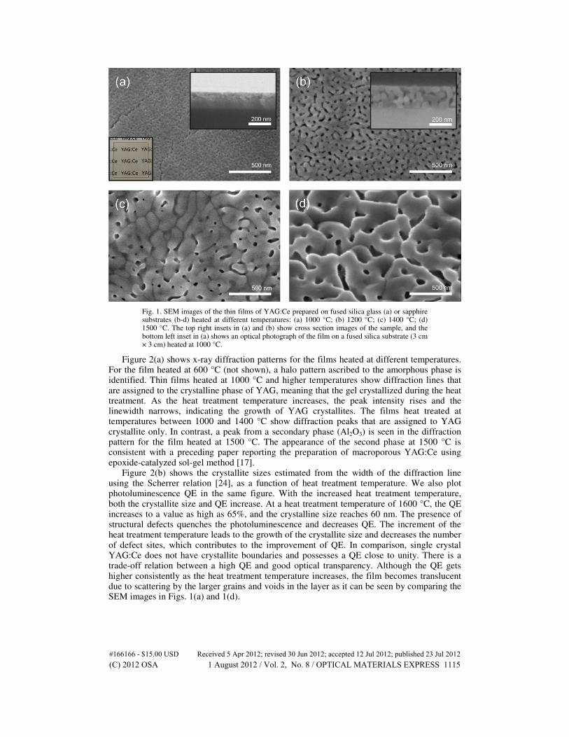
Fig. 1. SEM images of the thin films of YAG:Ce prepared on fused silica glass (a) or sapphire substrates (b-d) heated at different temperatures: (a) 1000 °C; (b) 1200 °C; (c) 1400 °C; (d) 1500 °C. The top right insets in (a) and (b) show cross section images of the sample, and the bottom left inset in (a) shows an optical photograph of the film on a fused silica substrate (3 cm × 3 cm) heated at 1000 °C.
Figure 2(a) shows x-ray diffraction patterns for the films heated at different temperatures. For the film heated at 600 °C (not shown), a halo pattern ascribed to the amorphous phase is identified. Thin films heated at 1000 °C and higher temperatures show diffraction lines that are assigned to the crystalline phase of YAG, meaning that the gel crystallized during the heat treatment. As the heat treatment temperature increases, the peak intensity rises and the linewidth narrows, indicating the growth of YAG crystallites. The films heat treated at temperatures between 1000 and 1400 °C show diffraction peaks that are assigned to YAG crystallite only. In contrast, a peak from a secondary phase (Al2O3) is seen in the diffraction pattern for the film heated at 1500 °C. The appearance of the second phase at 1500 °C is consistent with a preceding paper reporting the preparation of macroporous YAG:Ce using epoxide-catalyzed sol-gel method [17].
Figure 2(b) shows the crystallite sizes estimated from the width of the diffraction line using the Scherrer relation [24], as a function of heat treatment temperature. We also plot photoluminescence QE in the same figure. With the increased heat treatment temperature, both the crystallite size and QE increase. At a heat treatment temperature of 1600 °C, the QE increases to a value as high as 65%, and the crystalline size reaches 60 nm. The presence of structural defects quenches the photoluminescence and decreases QE. The increment of the heat treatment temperature leads to the growth of the crystallite size and decreases the number of defect sites, which contributes to the improvement of QE. In comparison, single crystal YAG:Ce does not have crystallite boundaries and possesses a QE close to unity. There is a trade-off relation between a high QE and good optical transparency. Although the QE gets higher consistently as the heat treatment temperature increases, the film becomes translucent due to scattering by the larger grains and voids in the layer as it can be seen by comparing the SEM images in Figs. 1(a) and 1(d).
#166166 - $15.00 USD Received 5 Apr 2012; revised 30 Jun 2012; accepted 12 Jul 2012; published 23 Jul 2012(C) 2012 OSA 1 August 2012 / Vol. 2, No. 8 / OPTICAL MATERIALS EXPRESS 1115
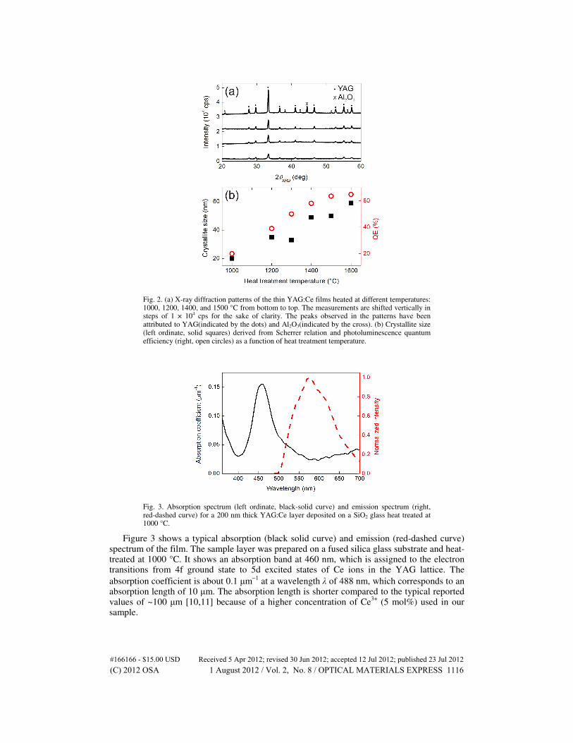
Fig. 2. (a) X-ray diffraction patterns of the thin YAG:Ce films heated at different temperatures: 1000, 1200, 1400, and 1500 °C from bottom to top. The measurements are shifted vertically in steps of 1 × 10⁴ cps for the sake of clarity. The peaks observed in the patterns have been attributed to YAG(indicated by the dots) and Al2O3(indicated by the cross). (b) Crystallite size (left ordinate, solid squares) derived from Scherrer relation and photoluminescence quantum efficiency (right, open circles) as a function of heat treatment temperature.
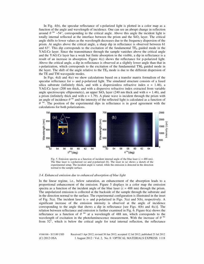
Fig. 3. Absorption spectrum (left ordinate, black-solid curve) and emission spectrum (right, red-dashed curve) for a 200 nm thick YAG:Ce layer deposited on a SiO2 glass heat treated at 1000 °C.
Figure 3 shows a typical absorption (black solid curve) and emission (red-dashed curve) spectrum of the film. The sample layer was prepared on a fused silica glass substrate and heat-treated at 1000 °C. It shows an absorption band at 460 nm, which is assigned to the electron transitions from 4f ground state to 5d excited states of Ce ions in the YAG lattice. The
absorption coefficient is about 0.1 µm−1
at a wavelength λ of 488 nm, which corresponds to an absorption length of 10 µm. The absorption length is shorter compared to the typical reported values of ~100 µm [10,11] because of a higher concentration of Ce
3+ (5 mol%) used in our
sample.
#166166 - $15.00 USD Received 5 Apr 2012; revised 30 Jun 2012; accepted 12 Jul 2012; published 23 Jul 2012(C) 2012 OSA 1 August 2012 / Vol. 2, No. 8 / OPTICAL MATERIALS EXPRESS 1116

The emission spectrum shown in Fig. 3 (red-dashed curve) was taken by exciting the sample at λ = 488 nm. Electrons excited to the 5d level of Ce ions decay nonradiatively through the excitation of phonons and finally transit radiatively to the 4f level of Ce ions, resulting in the broad emission centered at 575 nm with a large Stokes shift as shown in Fig. 3.
3.3. Enhanced absorption due to coupling of light into waveguide modes
In order to enhance the optical absorption in the thin YAG:Ce layer and increase the emission, we have coupled the excitation light into a waveguide mode by using the attenuated reflectance method. Waveguide modes are evanescent in the direction perpendicular to the waveguide. Therefore, they cannot be excited directly by far-field illumination. Briefly, the principle of prism coupling method is as follows (details can be found elsewhere [25]): An evanescent wave penetrates through the interface between the prism and the sample for angles of incidence larger than the critical angle of total internal reflection. The transmitted amplitude can couple to the guided mode in the layer for certain angles of incidence, leading to a reduction of the specular reflection.
Fig. 4. (a) Schematic illustration of the experimental setup used to couple incident light into the YAG:Ce thin layer. As a sample, we used the YAG:Ce layer (thickness = 200 nm) on the fused silica glass substrate heat treated at 1000 °C with a SiO2 layer (thickness = 240 nm) sputter-deposited on top. Experimental specular reflectance spectra as a function of incident internal angle for s-polarized (b) and p-polarized (c) light. Calculated specular reflectance spectra as a function of incident internal angle for s- polarized (d) and p- polarized (e) light.
The experimental configuration is schematically shown in Fig. 4(a). For the measurement, a SiO2 layer (240 nm) was sputtered on top of the YAG:Ce layer (200 nm) made on a fused silica substrate heat-treated at 1000 °C. A fused silica substrate was used in these measurements because of its lower refractive index compared to the YAG:Ce layer, which has a refractive index of n = 1.70 at λ = 488 nm as extracted from variable angle spectroscopic ellipsometry. Waveguide modes cannot be supported in a YAG:Ce layer when it is surrounded by sapphire because of its high refractive index (n = 1.78 at λ = 488 nm). The sample was illuminated with a collimated white light beam through the prism with an internal angle of incidence θ
inc and the specular reflectance was collected as a function of θ
inc.
#166166 - $15.00 USD Received 5 Apr 2012; revised 30 Jun 2012; accepted 12 Jul 2012; published 23 Jul 2012(C) 2012 OSA 1 August 2012 / Vol. 2, No. 8 / OPTICAL MATERIALS EXPRESS 1117
In Fig. 4(b), the specular reflectance of s-polarized light is plotted in a color map as a function of the angle and wavelength of incidence. One can see an abrupt change in reflection around θ
inc ~54°, corresponding to the critical angle. Above this angle the incident light is
totally internal reflected at the interface between the prism and the SiO2 layer. The critical angle shifts to lower values as the wavelength decreases due to the frequency dispersion of the prism. At angles above the critical angle, a sharp dip in reflectance is observed between 61 and 63°. This dip corresponds to the excitation of the fundamental TE0 guided mode in the YAG:Ce layer. Since the transmittance through the sample vanishes above the critical angle and the YAG:Ce layer has a weak but finite absorption in the visible, a dip in reflectance is a result of an increase in absorption. Figure 4(c) shows the reflectance for p-polarized light. Above the critical angle, a dip in reflectance is observed at a slightly lower angle than that in s-polarization, which corresponds to the excitation of the fundamental TM0 guided mode in the layer. The shift of the angle relative to the TE0 mode is due to the different dispersion of the TE and TM waveguide modes.
In Figs. 4(d) and 4(e) we show calculations based on a transfer matrix formalism of the specular reflectance for s- and p-polarized light. The simulated structure consists of a fused silica substrate (infinitely thick, and with a dispersionless refractive index n = 1.46), a YAG:Ce layer (200 nm thick, and with a dispersive refractive index extracted from variable angle spectroscopic ellipsometry), an upper SiO2 layer (240 nm thick and with n = 1.46), and a prism (infinitely thick and with n = 1.79). A plane wave is incident through the prism with an angle of incidence θ
inc and the intensity of the reflected light is calculated as a function of
θ inc
. The position of the experimental dips in reflectance is in good agreement with the calculations for both polarizations.
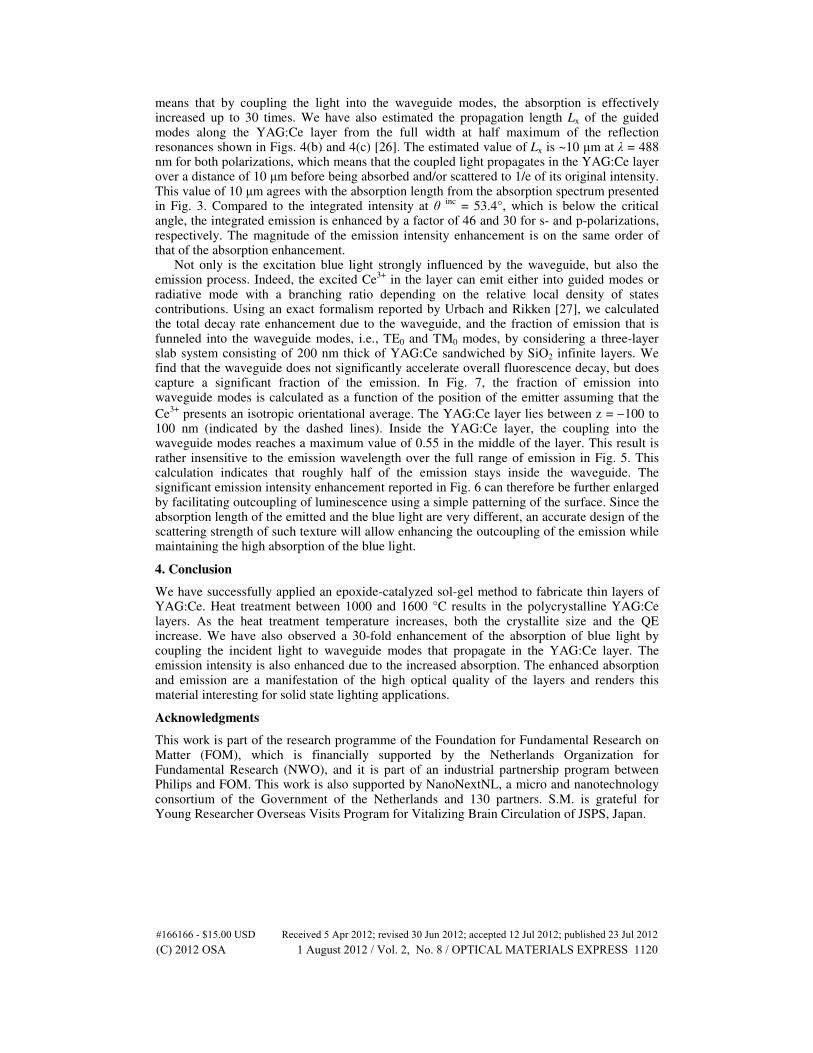
Fig. 5. Emission spectra as a function of incident internal angle of the blue laser (λ = 488 nm). The blue laser is s-polarized (a) and p-polarized (b). The inset in (a) shows a sketch of the experimental setup. The incident angle is varied, while the emission is detected in the direction normal to the sample surface.
3.4. Enhanced emission due to enhanced absorption of blue light
In the linear regime, i.e., below saturation, an enhancement of the absorption leads to a proportional enhancement of the emission. Figure 5 displays in a color map the emission spectra as a function of the incident angle of the blue laser (λ = 488 nm) through the prism. The unpolarized emission is collected at the backside of the sample through the substrate and in the direction normal to the surface. The experimental configuration is illustrated in the inset of Fig. 5(a). The incident laser is s- and p-polarized in Figs. 5(a) and 5(b), respectively. A significant increase of the emission intensity is observed at the angle of incidence corresponding to the angle that shows a dip in reflectance [see Figs. 4(b) and 4(c)]. The relation between reflectance and emission is further examined in Fig. 6. Figure 6(a) shows the reflectance as a function of θ
inc at a wavelength of 488 nm, which corresponds to the
wavelength of excitation in the photoluminescence measurement. With the increase of θ inc
from 52°, which is below the critical angle for total internal reflection, the reflectance
#166166 - $15.00 USD Received 5 Apr 2012; revised 30 Jun 2012; accepted 12 Jul 2012; published 23 Jul 2012(C) 2012 OSA 1 August 2012 / Vol. 2, No. 8 / OPTICAL MATERIALS EXPRESS 1118

increases. At 62.4 and 60.3° for s-(black circles) and p-(grey squares) polarization, respectively, the reflectance presents a local minimum due to the excitation of the TE0 and TM0 modes. In Fig. 6(b), the emission intensity, integrated from λ = 500 to 700 nm, is plotted as a function of θ
inc of the blue laser. The emission intensity shows a maximum at θ
inc that
corresponds to the minimum in reflectance for both s-(black curve) and p-(grey curve) polarizations.
Fig. 6. (a) Specular reflectance of a 200 nm thick layer of YAG:Ce at a wavelength of 488 nm for s-polarized (black circles) and p-polarized (grey squares) light. (b) Integrated emission intensity between 500 and 700 nm as a function of incident angle of the blue laser (λ = 488 nm) for s-polarized (black) and p-polarized light (grey).
Fig. 7. Fraction of the emission (λ = 580 nm) that is funneled into the waveguide modes (TE0 and TM0 modes) as a function of the position of the emitter, averaged over all orientations of the emitter. The dashed lines indicate the position of the YAG:Ce layer. The inset shows a sketch of the three-layer system used in the calculation, which ignores the evanescently coupled prism but contains all layers of the sample.
The correspondence between the dips in reflectance and the peaks in the integrated emission intensity suggests that the enhanced emission is due to enhanced absorption. The minimum reflectance is as low as 0.56 for both polarizations, meaning that the absorptance is 0.44, if no light is transmitted through the sample. The absorption length that corresponds to an absorptance of 0.44 at λ = 488 nm is 0.35 µm, as calculated considering the Lambert-Beer law. This value is far shorter than the value of 10 µm indicated in Fig. 3 for YAG:Ce, which
#166166 - $15.00 USD Received 5 Apr 2012; revised 30 Jun 2012; accepted 12 Jul 2012; published 23 Jul 2012(C) 2012 OSA 1 August 2012 / Vol. 2, No. 8 / OPTICAL MATERIALS EXPRESS 1119
means that by coupling the light into the waveguide modes, the absorption is effectively increased up to 30 times. We have also estimated the propagation length Lx of the guided modes along the YAG:Ce layer from the full width at half maximum of the reflection resonances shown in Figs. 4(b) and 4(c) [26]. The estimated value of Lx is ~10 µm at λ = 488 nm for both polarizations, which means that the coupled light propagates in the YAG:Ce layer over a distance of 10 µm before being absorbed and/or scattered to 1/e of its original intensity. This value of 10 µm agrees with the absorption length from the absorption spectrum presented in Fig. 3. Compared to the integrated intensity at θ
inc = 53.4°, which is below the critical
angle, the integrated emission is enhanced by a factor of 46 and 30 for s- and p-polarizations, respectively. The magnitude of the emission intensity enhancement is on the same order of that of the absorption enhancement.
Not only is the excitation blue light strongly influenced by the waveguide, but also the emission process. Indeed, the excited Ce
3+ in the layer can emit either into guided modes or
radiative mode with a branching ratio depending on the relative local density of states contributions. Using an exact formalism reported by Urbach and Rikken [27], we calculated the total decay rate enhancement due to the waveguide, and the fraction of emission that is funneled into the waveguide modes, i.e., TE0 and TM0 modes, by considering a three-layer slab system consisting of 200 nm thick of YAG:Ce sandwiched by SiO2 infinite layers. We find that the waveguide does not significantly accelerate overall fluorescence decay, but does capture a significant fraction of the emission. In Fig. 7, the fraction of emission into waveguide modes is calculated as a function of the position of the emitter assuming that the
Ce3+
presents an isotropic orientational average. The YAG:Ce layer lies between z = −100 to 100 nm (indicated by the dashed lines). Inside the YAG:Ce layer, the coupling into the waveguide modes reaches a maximum value of 0.55 in the middle of the layer. This result is rather insensitive to the emission wavelength over the full range of emission in Fig. 5. This calculation indicates that roughly half of the emission stays inside the waveguide. The significant emission intensity enhancement reported in Fig. 6 can therefore be further enlarged by facilitating outcoupling of luminescence using a simple patterning of the surface. Since the absorption length of the emitted and the blue light are very different, an accurate design of the scattering strength of such texture will allow enhancing the outcoupling of the emission while maintaining the high absorption of the blue light.
4. Conclusion
We have successfully applied an epoxide-catalyzed sol-gel method to fabricate thin layers of YAG:Ce. Heat treatment between 1000 and 1600 °C results in the polycrystalline YAG:Ce layers. As the heat treatment temperature increases, both the crystallite size and the QE increase. We have also observed a 30-fold enhancement of the absorption of blue light by coupling the incident light to waveguide modes that propagate in the YAG:Ce layer. The emission intensity is also enhanced due to the increased absorption. The enhanced absorption and emission are a manifestation of the high optical quality of the layers and renders this material interesting for solid state lighting applications.
Acknowledgments
This work is part of the research programme of the Foundation for Fundamental Research on Matter (FOM), which is financially supported by the Netherlands Organization for Fundamental Research (NWO), and it is part of an industrial partnership program between Philips and FOM. This work is also supported by NanoNextNL, a micro and nanotechnology consortium of the Government of the Netherlands and 130 partners. S.M. is grateful for Young Researcher Overseas Visits Program for Vitalizing Brain Circulation of JSPS, Japan.
#166166 - $15.00 USD Received 5 Apr 2012; revised 30 Jun 2012; accepted 12 Jul 2012; published 23 Jul 2012(C) 2012 OSA 1 August 2012 / Vol. 2, No. 8 / OPTICAL MATERIALS EXPRESS 1120


![^Q L:HO = ;T;; pK=QC CPO? lHC;5O - ag.musin.de · ^q l:ho = ;t;; pk=qc cpo? lhc;5o o kdkm o ^q lt:=akoho?- okdo b?kd5o==kd 9c d ... po? z: ?= ;;loi o | kd okdog fcc=tq lo?]o dm ohgtdd`](https://img.pdfslide.org/doc/110x75/5b85e81c7f8b9af12d8bca16/q-lho-t-pkqc-cpo-lhc5o-agmusinde-q-lho-t-pkqc-cpo-lhc5o.jpg)


![Ofittt ntttt jttfd]rlflttlftl DOll UttlOrnltlltl.Ofittt ntttt jttfd]rlflttlftl DOll UttlOrnltlltl. 3m 3ufi be6 l.lcrgallgellell 3al)reß wurbe \)on hem Sl)iteftor !let 2lu~grabullgell](https://img.pdfslide.org/doc/110x75/60c88318556f881aaa55d4e5/ofittt-ntttt-jttfdrlflttlftl-doll-ofittt-ntttt-jttfdrlflttlftl-doll-uttlornltlltl.jpg)
![rOMOK=;O?:DM N ? ] OQLDKI · 2016. 3. 11. · tdo?itdd;o ro?t;:dm==;ohho =okdm \dp t:q l- 8o? =kq l ro? pko n ?o k| 5o k;tdmorc;o kdnc?gko? od 8khh- k=; jo| po? 5o k; 8khhi cggodm](https://img.pdfslide.org/doc/110x75/60909e2c0b0e8a5336368b1a/romokodm-n-oqldki-2016-3-11-tdoitddo-rotdmohho-okdm-dp-tq.jpg)

![Ultra-thin aluminium oxide films deposited by plasma- enhanced atomic layer deposition ... · 3 deposited by plasma-enhanced ALD, from [Al(CH 3) 3] with an O 2 plasma, as a protective](https://img.pdfslide.org/doc/110x75/611d563f261d0233ff71de6c/ultra-thin-aluminium-oxide-films-deposited-by-plasma-enhanced-atomic-layer-deposition.jpg)